Plenary Compound Semiconductor Week May 29 th 2018
![[110] gives more on-current than [100] high confinement mass low transport mass P. Long [110] gives more on-current than [100] high confinement mass low transport mass P. Long](https://slidetodoc.com/presentation_image_h2/5480810598aae329e057e5a19e6840b4/image-8.jpg)


- Slides: 54

Plenary, Compound Semiconductor Week, May 29 th, 2018 - June 1 st, 2018, MIT Transistors: mm-Wave and Low-Power VLSI Mark Rodwell, UCSB Low-voltage devices B. Markman, H. -Y. Tseng, S. Brunelli, S. Choi, A. Goswani, C. Palmstrøm, J. Klamkin: UCSB P. Long, J. Huang, E. Wilson, S. Mehrotra, C. Y. -Chen, M. Povolotskyi, G. Klimeck: Purdue In. P HBT: Y. Fang, J. Rode*: UCSB In. P MOS-HEMT J. Wu: UCSB Millimeter-wave systems design, mm-wave ICs. M. Abdelghany, A. Farid, A. Ahmed, U. Madhow : UCSB A. Niknejad: UC Berkeley Now with *Intel

VLSI Transistors 2

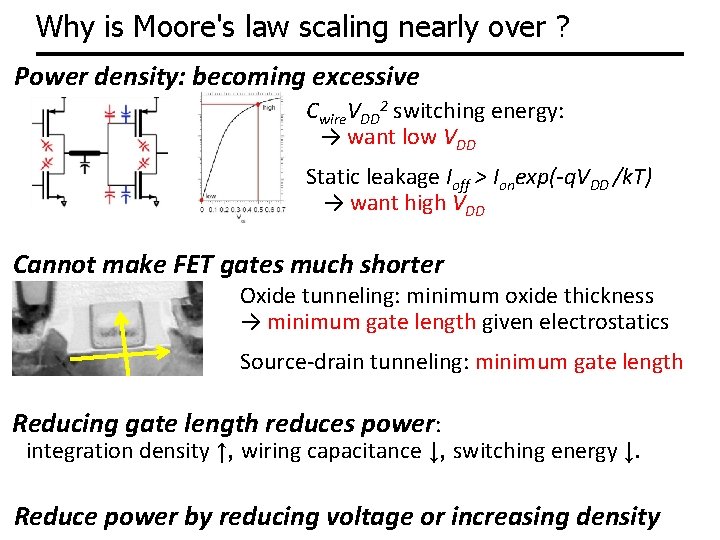
Why is Moore's law scaling nearly over ? Power density: becoming excessive Cwire. VDD 2 switching energy: → want low VDD Static leakage Ioff > Ionexp(-q. VDD /k. T) → want high VDD Cannot make FET gates much shorter Oxide tunneling: minimum oxide thickness → minimum gate length given electrostatics Source-drain tunneling: minimum gate length Reducing gate length reduces power: integration density ↑, wiring capacitance ↓, switching energy ↓. Reduce power by reducing voltage or increasing density

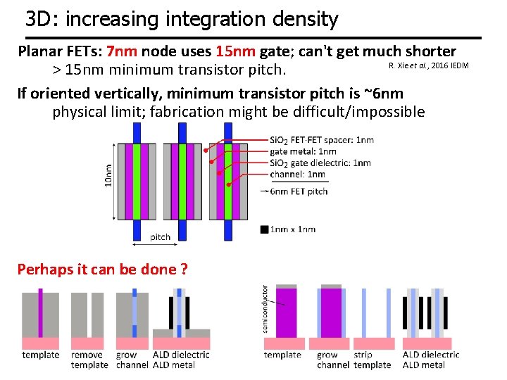
3 D: increasing integration density Planar FETs: 7 nm node uses 15 nm gate; can't get much shorter R. Xie et al. , 2016 IEDM > 15 nm minimum transistor pitch. If oriented vertically, minimum transistor pitch is ~6 nm physical limit; fabrication might be difficult/impossible Perhaps it can be done ?

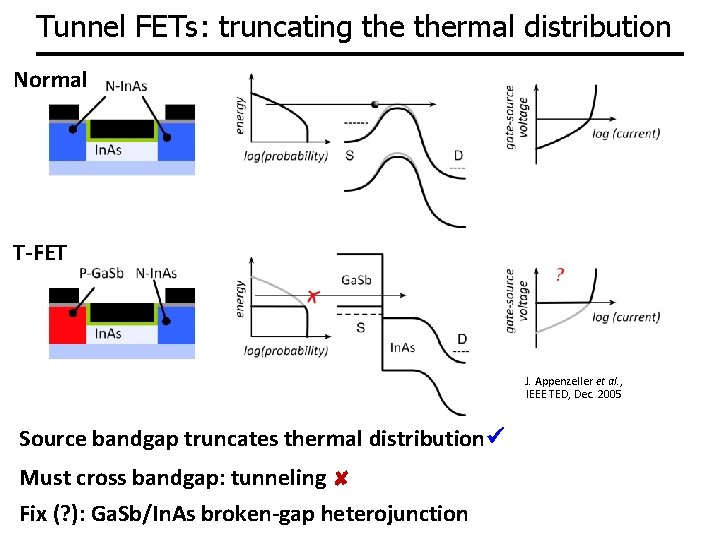
Tunnel FETs: truncating thermal distribution Normal T-FET J. Appenzeller et al. , IEEE TED, Dec. 2005 Source bandgap truncates thermal distribution Must cross bandgap: tunneling ✘ Fix (? ): Ga. Sb/In. As broken-gap heterojunction

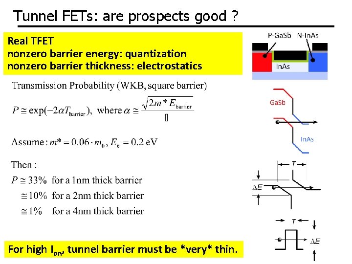
Tunnel FETs: are prospects good ? Real TFET nonzero barrier energy: quantization nonzero barrier thickness: electrostatics For high Ion, tunnel barrier must be *very* thin.

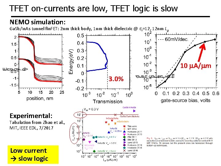
TFET on-currents are low, TFET logic is slow NEMO simulation: Ga. Sb/In. As tunnel fin. FET: 2 nm thick body, 1 nm thick dielectric @ er=12, 12 nm Lg 10 m. A/mm 3. 0% Experimental: Tabulation from Zhao et al. , MIT, IEEE EDL, 7/2017 Low current → slow logic
![110 gives more oncurrent than 100 high confinement mass low transport mass P Long [110] gives more on-current than [100] high confinement mass low transport mass P. Long](https://slidetodoc.com/presentation_image_h2/5480810598aae329e057e5a19e6840b4/image-8.jpg)
[110] gives more on-current than [100] high confinement mass low transport mass P. Long et al. , EDL 3/2016 low confinement mass high transport mass

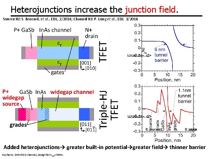
Heterojunctions increase the junction field. Source HJ: S. Brocard, et al. , EDL, 2/2014; Channel HJ: P. Long et al. , EDL 3/2016 Added heterojunctions→ greater built-in potential→greater field→ thinner barrier Key facts: 2 nm thick channel, design for VDD=70 m. V.

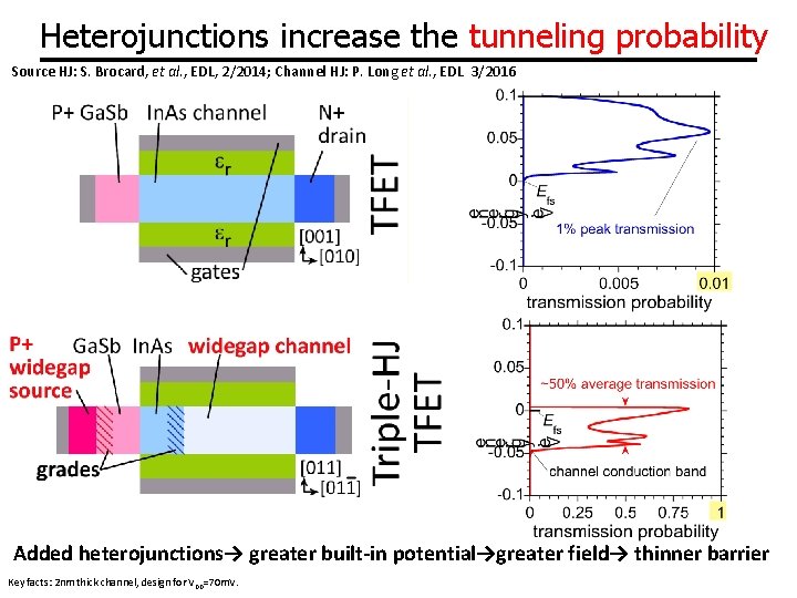
Heterojunctions increase the tunneling probability Source HJ: S. Brocard, et al. , EDL, 2/2014; Channel HJ: P. Long et al. , EDL 3/2016 Added heterojunctions→ greater built-in potential→greater field→ thinner barrier Key facts: 2 nm thick channel, design for VDD=70 m. V.

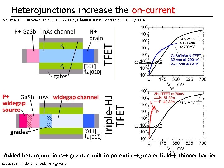
Heterojunctions increase the on-current Source HJ: S. Brocard, et al. , EDL, 2/2014; Channel HJ: P. Long et al. , EDL 3/2016 Added heterojunctions→ greater built-in potential→greater field→ thinner barrier Key facts: 2 nm thick channel, design for VDD=70 m. V.

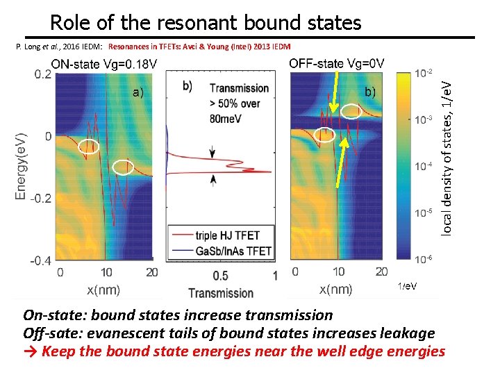
Role of the resonant bound states local density of states, 1/e. V P. Long et al. , 2016 IEDM: Resonances in TFETs: Avci & Young (Intel) 2013 IEDM On-state: bound states increase transmission Off-sate: evanescent tails of bound states increases leakage → Keep the bound state energies near the well edge energies

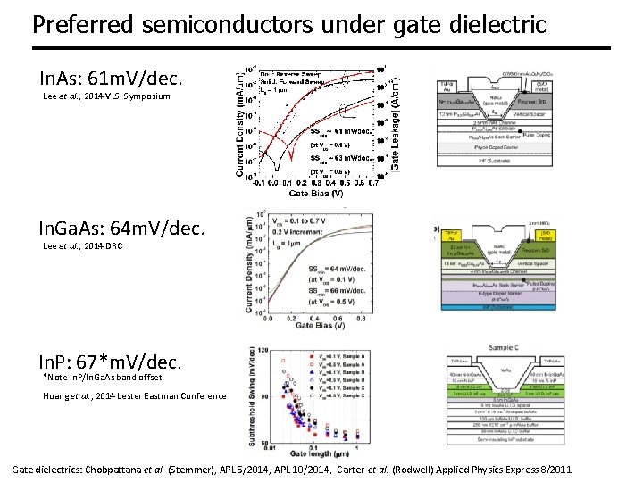
Preferred semiconductors under gate dielectric In. As: 61 m. V/dec. Lee et al. , 2014 VLSI Symposium In. Ga. As: 64 m. V/dec. Lee et al. , 2014 DRC In. P: 67*m. V/dec. *Note In. P/In. Ga. As band offset Huang et al. , 2014 Lester Eastman Conference Gate dielectrics: Chobpattana et al. (Stemmer), APL 5/2014, APL 10/2014, Carter et al. (Rodwell) Applied Physics Express 8/2011

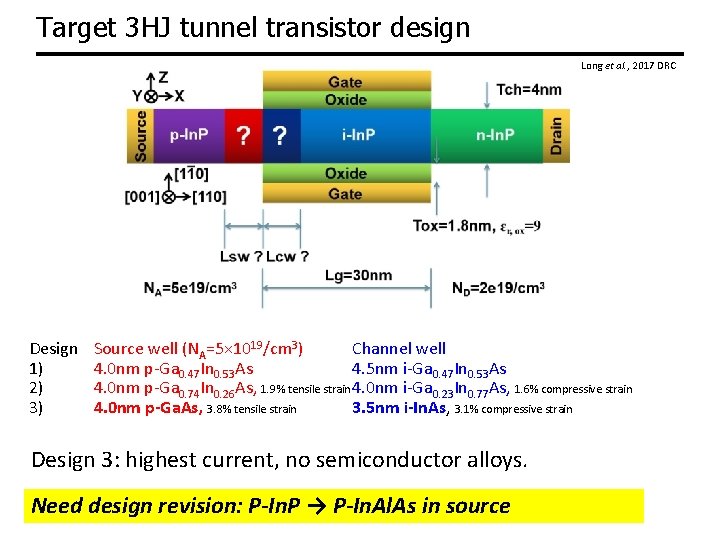
Target 3 HJ tunnel transistor design Long et al. , 2017 DRC NA=5× 10¹⁹/cm 3 Design 1) 2) 3) Source well (NA=5× 10¹⁹/cm 3) Channel well 4. 0 nm p-Ga 0. 47 In 0. 53 As 4. 5 nm i-Ga 0. 47 In 0. 53 As 4. 0 nm p-Ga 0. 74 In 0. 26 As, 1. 9% tensile strain 4. 0 nm i-Ga 0. 23 In 0. 77 As, 1. 6% compressive strain 4. 0 nm p-Ga. As, 3. 8% tensile strain 3. 5 nm i-In. As, 3. 1% compressive strain Design 3: highest current, no semiconductor alloys. Need design revision: P-In. P → P-In. Al. As in source

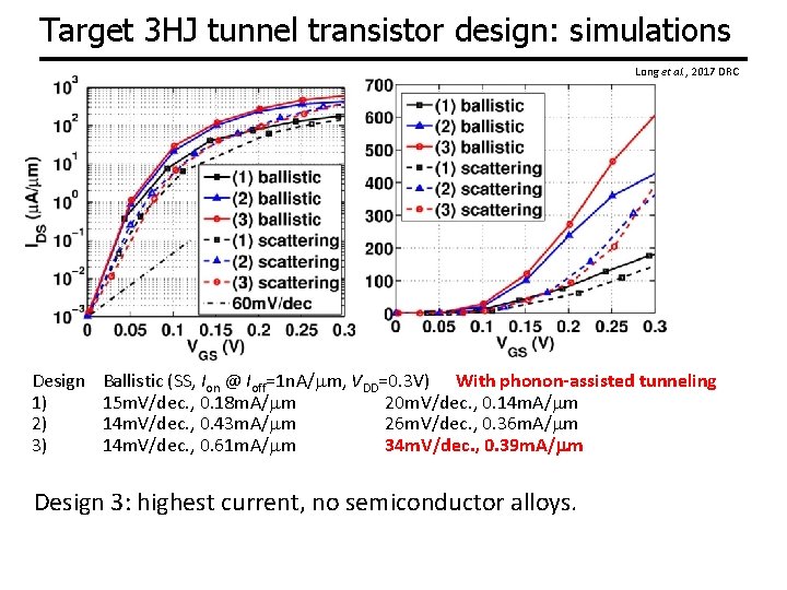
Target 3 HJ tunnel transistor design: simulations Long et al. , 2017 DRC Design 1) 2) 3) Ballistic (SS, Ion @ Ioff=1 n. A/mm, VDD=0. 3 V) With phonon-assisted tunneling 15 m. V/dec. , 0. 18 m. A/mm 20 m. V/dec. , 0. 14 m. A/mm 14 m. V/dec. , 0. 43 m. A/mm 26 m. V/dec. , 0. 36 m. A/mm 14 m. V/dec. , 0. 61 m. A/mm 34 m. V/dec. , 0. 39 m. A/mm Design 3: highest current, no semiconductor alloys.

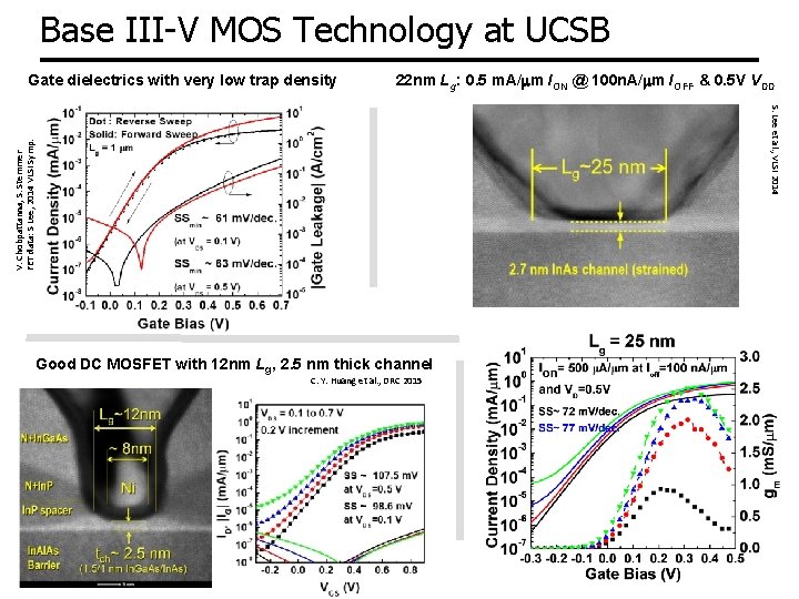
Base III-V MOS Technology at UCSB Gate dielectrics with very low trap density 22 nm Lg: 0. 5 m. A/mm ION @ 100 n. A/mm IOFF & 0. 5 V VDD V. Chobpattanna, S. Stemmer FET data: S Lee, 2014 VLSI Symp. S. Lee et al. , VLSI 2014 Good DC MOSFET with 12 nm Lg, 2. 5 nm thick channel C. Y. Huang et al. , DRC 2015

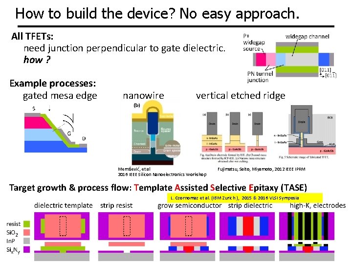
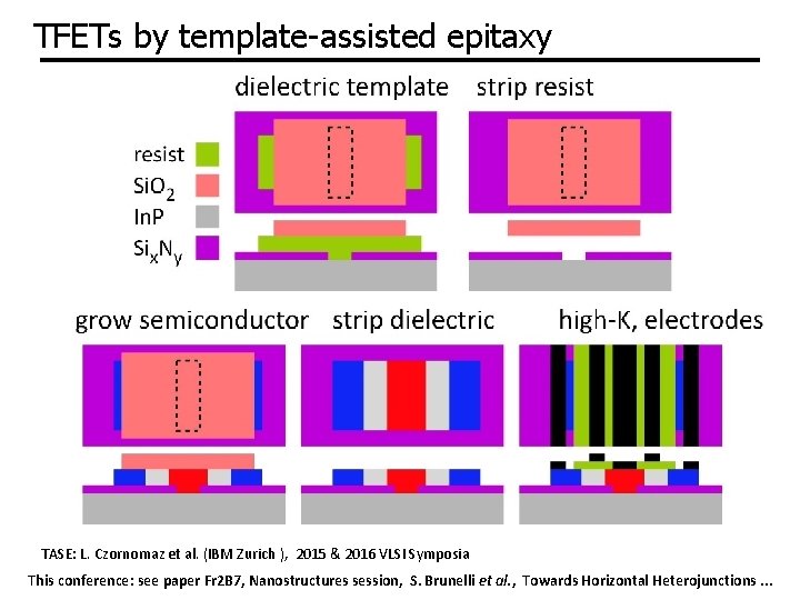
How to build the device? No easy approach. All TFETs: need junction perpendicular to gate dielectric. how ? Example processes: gated mesa edge nanowire vertical etched ridge Memišević, et al 2016 IEEE Silicon Nanoelectronics Workshop Fujimatsu, Saito, Miyamoto, 2012 IEEE IPRM Target growth & process flow: Template Assisted Selective Epitaxy (TASE) L. Czornomaz et al. (IBM Zurich ), 2015 & 2016 VLSI Symposia

TFETs by template-assisted epitaxy TASE: L. Czornomaz et al. (IBM Zurich ), 2015 & 2016 VLSI Symposia This conference: see paper Fr 2 B 7, Nanostructures session, S. Brunelli et al. , Towards Horizontal Heterojunctions. . .

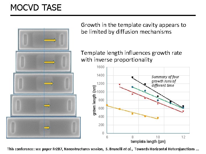
MOCVD TASE Growth in the template cavity appears to be limited by diffusion mechanisms Template length influences growth rate with inverse proportionality 1600 grown length (nm) 1400 Summary of four growth runs of different time 1200 1000 800 600 400 200 0 6 8 10 12 template length (µm) This conference: see paper Fr 2 B 7, Nanostructures session, S. Brunelli et al. , Towards Horizontal Heterojunctions. . .

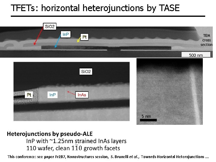
TFETs: horizontal heterojunctions by TASE This conference: see paper Fr 2 B 7, Nanostructures session, S. Brunelli et al. , Towards Horizontal Heterojunctions. . .

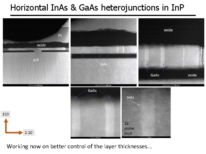
Horizontal In. As & Ga. As heterojunctions in In. P Working now on better control of the layer thicknesses. . .

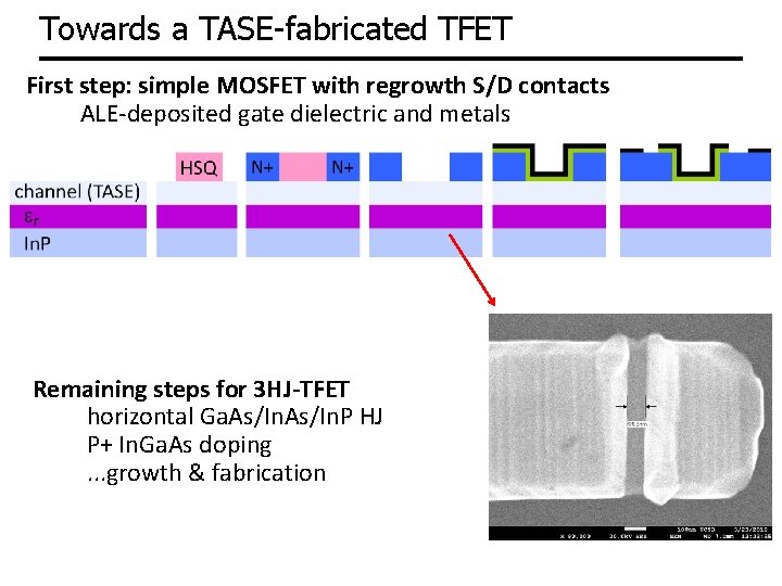
Towards a TASE-fabricated TFET First step: simple MOSFET with regrowth S/D contacts ALE-deposited gate dielectric and metals Remaining steps for 3 HJ-TFET horizontal Ga. As/In. P HJ P+ In. Ga. As doping. . . growth & fabrication

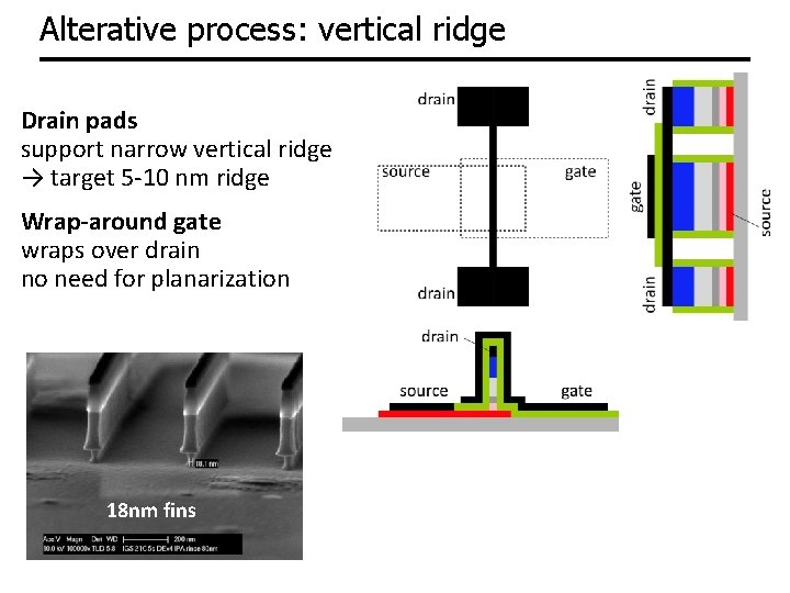
Alterative process: vertical ridge Drain pads support narrow vertical ridge → target 5 -10 nm ridge Wrap-around gate wraps over drain no need for planarization 18 nm fins

THz transistors 24

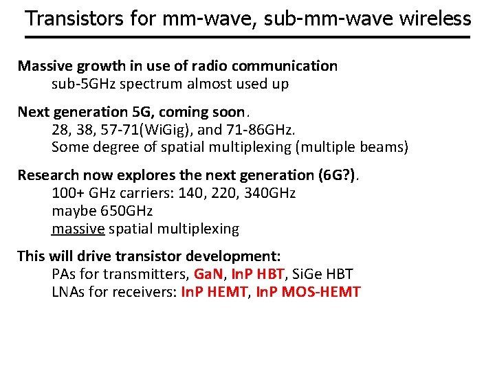
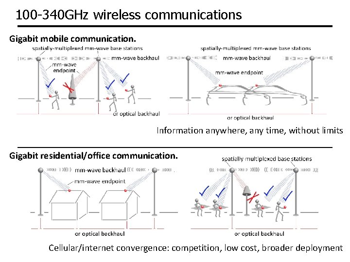
Transistors for mm-wave, sub-mm-wave wireless Massive growth in use of radio communication sub-5 GHz spectrum almost used up Next generation 5 G, coming soon. 28, 38, 57 -71(Wi. Gig), and 71 -86 GHz. Some degree of spatial multiplexing (multiple beams) Research now explores the next generation (6 G? ). 100+ GHz carriers: 140, 220, 340 GHz maybe 650 GHz massive spatial multiplexing This will drive transistor development: PAs for transmitters, Ga. N, In. P HBT, Si. Ge HBT LNAs for receivers: In. P HEMT, In. P MOS-HEMT

100 -340 GHz wireless communications Gigabit mobile communication. Information anywhere, any time, without limits Gigabit residential/office communication. Cellular/internet convergence: competition, low cost, broader deployment

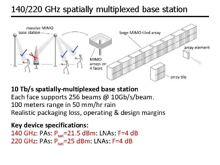
140/220 GHz spatially multiplexed base station 10 Tb/s spatially-multiplexed base station Each face supports 256 beams @ 10 Gb/s/beam. 100 meters range in 50 mm/hr rain Realistic packaging loss, operating & design margins Key device specifications: 140 GHz: PAs: Psat=21. 5 d. Bm: LNAs: F=4 d. B 220 GHz: PAs: Psat=25 d. Bm: LNAs: F=4 d. B

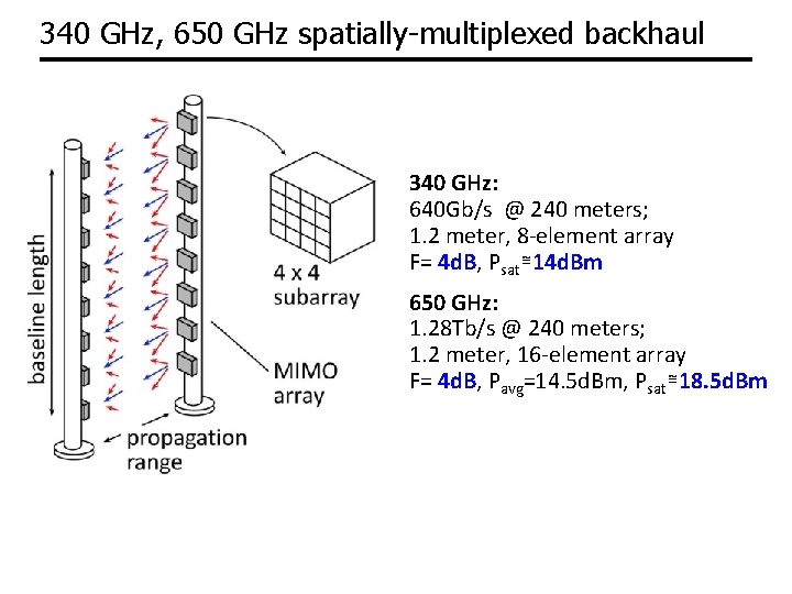
340 GHz, 650 GHz spatially-multiplexed backhaul 340 GHz: 640 Gb/s @ 240 meters; 1. 2 meter, 8 -element array F= 4 d. B, Psat≅14 d. Bm 650 GHz: 1. 28 Tb/s @ 240 meters; 1. 2 meter, 16 -element array F= 4 d. B, Pavg=14. 5 d. Bm, Psat≅18. 5 d. Bm

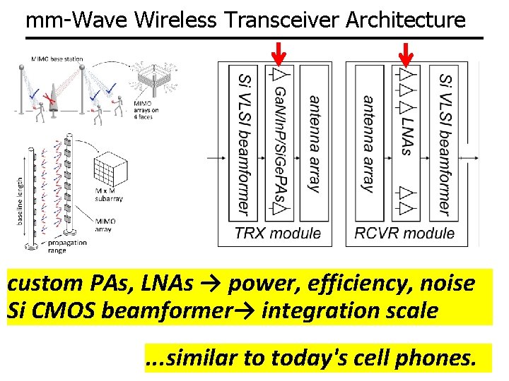
mm-Wave Wireless Transceiver Architecture custom PAs, LNAs → power, efficiency, noise Si CMOS beamformer→ integration scale. . . similar to today's cell phones.

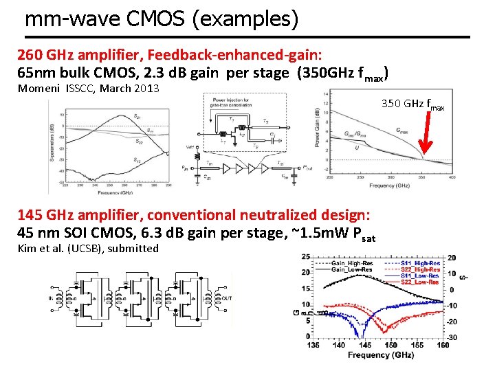
mm-wave CMOS (examples) 260 GHz amplifier, Feedback-enhanced-gain: 65 nm bulk CMOS, 2. 3 d. B gain per stage (350 GHz fmax) Momeni ISSCC, March 2013 350 GHz fmax 145 GHz amplifier, conventional neutralized design: 45 nm SOI CMOS, 6. 3 d. B gain per stage, ~1. 5 m. W Psat Kim et al. (UCSB), submitted

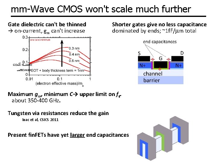
mm-Wave CMOS won't scale much further Gate dielectric can't be thinned → on-current, gm can't increase Shorter gates give no less capacitance dominated by ends; ~1 f. F/mm total Maximum gm, minimum C→ upper limit on ft. about 350 -400 GHz. Tungsten via resistances reduce the gain Inac et al, CSICS 2011 Present fin. FETs have yet larger end capacitances

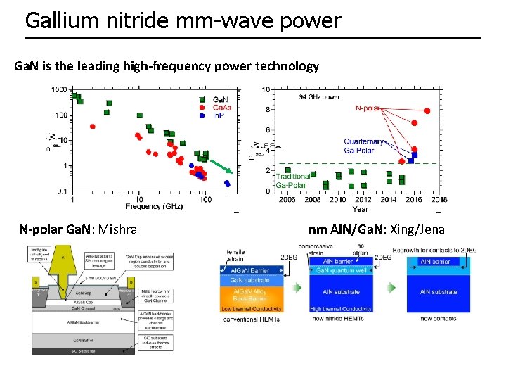
Gallium nitride mm-wave power Ga. N is the leading high-frequency power technology N-polar Ga. N: Mishra nm Al. N/Ga. N: Xing/Jena

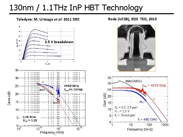
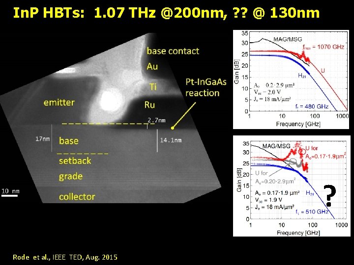
130 nm / 1. 1 THz In. P HBT Technology Teledyne: M. Urteaga et al: 2011 DRC 3. 5 V breakdown Rode (UCSB), IEEE TED, 2015

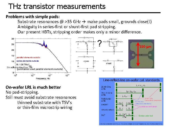
THz transistor measurements Problems with simple pads: Substrate resonances @ >35 GHz → make pads small, grounds close(!) Ambiguity in series-first or shunt-first pad stripping. Our present HBTs, stripping order makes only a minor difference. 220 mm (publication used parallel elements outside) On-wafer LRL is much better No pad-stripping. Still must avoid substrate resonances thinned substrate with TSV's or thin-film microstrip wiring

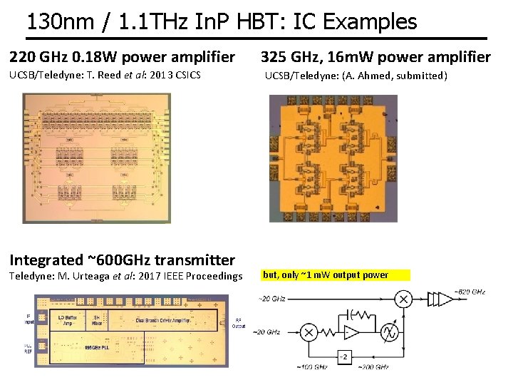
130 nm / 1. 1 THz In. P HBT: IC Examples 220 GHz 0. 18 W power amplifier UCSB/Teledyne: T. Reed et al: 2013 CSICS Integrated ~600 GHz transmitter Teledyne: M. Urteaga et al: 2017 IEEE Proceedings 325 GHz, 16 m. W power amplifier UCSB/Teledyne: (A. Ahmed, submitted) but, only ~1 m. W output power

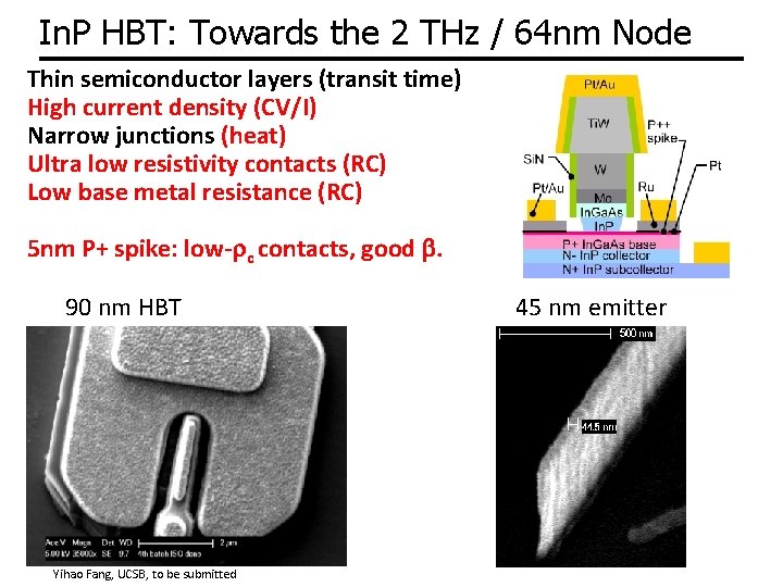
In. P HBT: Towards the 2 THz / 64 nm Node Thin semiconductor layers (transit time) High current density (CV/I) Narrow junctions (heat) Ultra low resistivity contacts (RC) Low base metal resistance (RC) 5 nm P+ spike: low-rc contacts, good b. 90 nm HBT Yihao Fang, UCSB, to be submitted 45 nm emitter

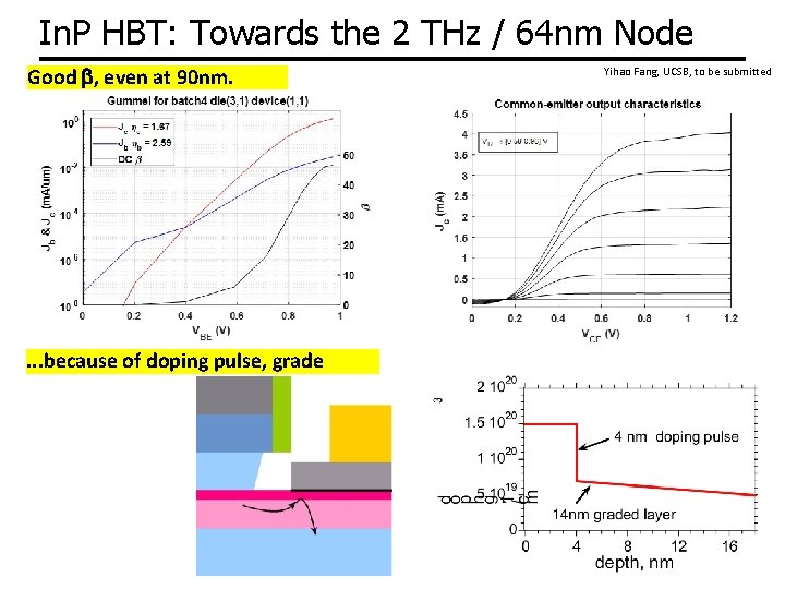
In. P HBT: Towards the 2 THz / 64 nm Node Good b, even at 90 nm. . because of doping pulse, grade Yihao Fang, UCSB, to be submitted

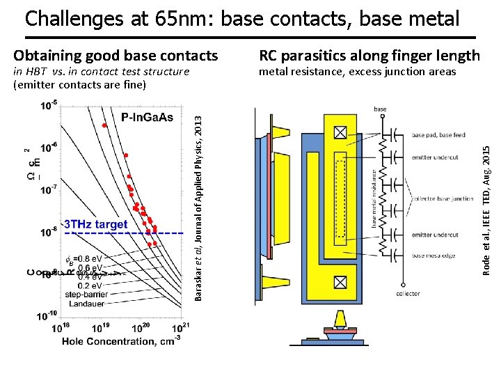
Challenges at 65 nm: base contacts, base metal Baraskar et al, Journal of Applied Physics, 2013 in HBT vs. in contact test structure (emitter contacts are fine) RC parasitics along finger length metal resistance, excess junction areas Rode et al. , IEEE TED, Aug. 2015 Obtaining good base contacts

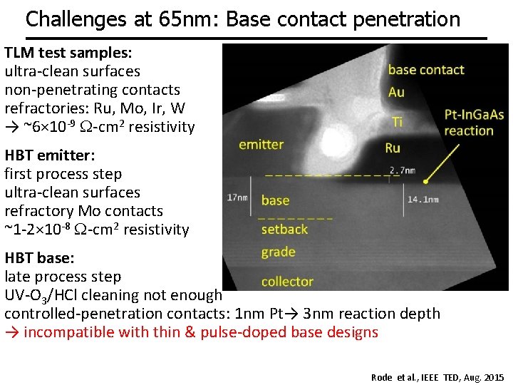
Challenges at 65 nm: Base contact penetration TLM test samples: ultra-clean surfaces non-penetrating contacts refractories: Ru, Mo, Ir, W → ~6× 10 -9 W-cm 2 resistivity HBT emitter: first process step ultra-clean surfaces refractory Mo contacts ~1 -2× 10 -8 W-cm 2 resistivity HBT base: late process step UV-O 3/HCl cleaning not enough controlled-penetration contacts: 1 nm Pt→ 3 nm reaction depth → incompatible with thin & pulse-doped base designs Rode et al. , IEEE TED, Aug. 2015

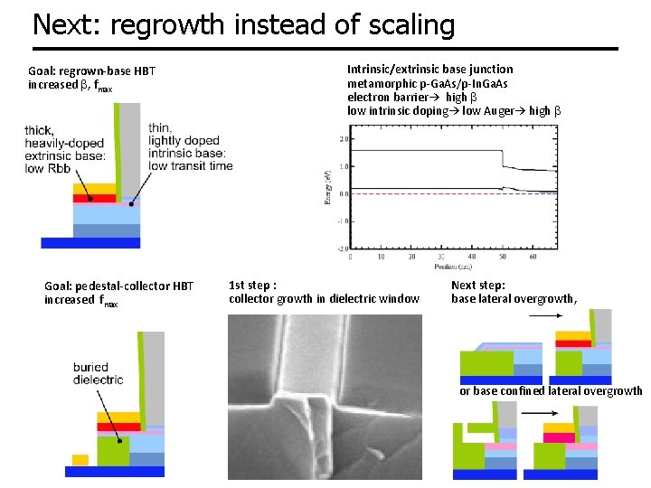
Next: regrowth instead of scaling Goal: regrown-base HBT increased b, fmax Goal: pedestal-collector HBT increased fmax Intrinsic/extrinsic base junction metamorphic p-Ga. As/p-In. Ga. As electron barrier→ high b low intrinsic doping→ low Auger→ high b 1 st step : collector growth in dielectric window Next step: base lateral overgrowth, or base confined lateral overgrowth

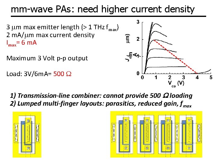
mm-wave PAs: need higher current density 3 mm max emitter length (> 1 THz fmax) 2 m. A/mm max current density Imax= 6 m. A Maximum 3 Volt p-p output Load: 3 V/6 m. A= 500 W 1) Transmission-line combiner: cannot provide 500 W loading 2) Lumped multi-finger layouts: parasitics, reduced gain, fmax

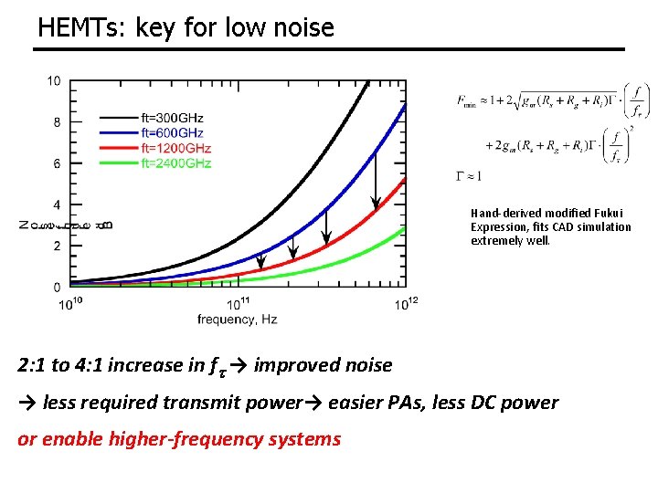
HEMTs: key for low noise Hand-derived modified Fukui Expression, fits CAD simulation extremely well. 2: 1 to 4: 1 increase in ft → improved noise → less required transmit power→ easier PAs, less DC power or enable higher-frequency systems

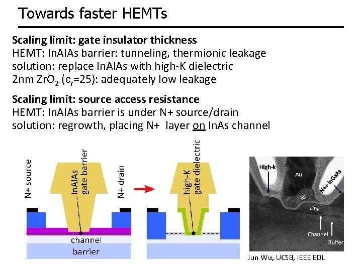
Towards faster HEMTs Scaling limit: gate insulator thickness HEMT: In. Al. As barrier: tunneling, thermionic leakage solution: replace In. Al. As with high-K dielectric 2 nm Zr. O 2 (er=25): adequately low leakage Scaling limit: source access resistance HEMT: In. Al. As barrier is under N+ source/drain solution: regrowth, placing N+ layer on In. As channel Jun Wu, UCSB, IEEE EDL

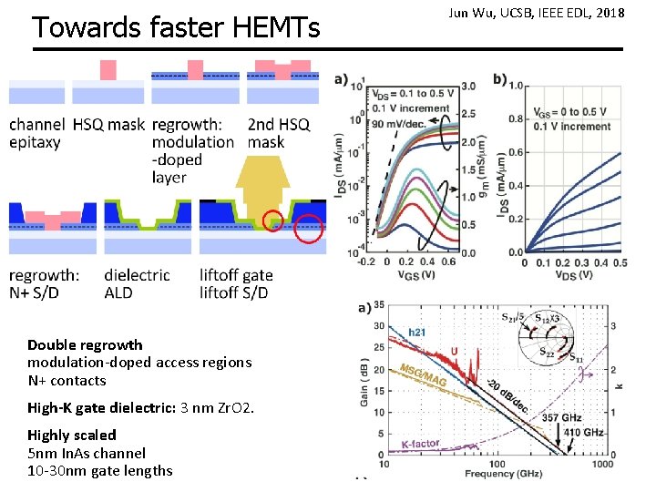
Towards faster HEMTs Double regrowth modulation-doped access regions N+ contacts High-K gate dielectric: 3 nm Zr. O 2. Highly scaled 5 nm In. As channel 10 -30 nm gate lengths Jun Wu, UCSB, IEEE EDL, 2018

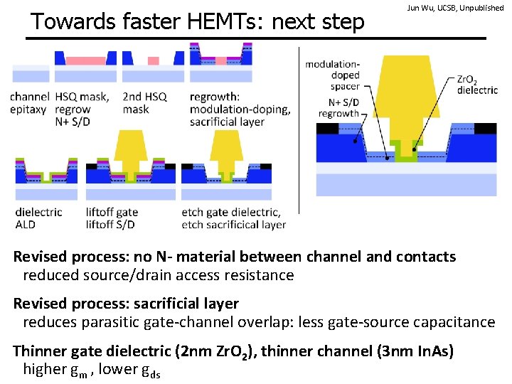
Towards faster HEMTs: next step Jun Wu, UCSB, Unpublished Revised process: no N- material between channel and contacts reduced source/drain access resistance Revised process: sacrificial layer reduces parasitic gate-channel overlap: less gate-source capacitance Thinner gate dielectric (2 nm Zr. O 2), thinner channel (3 nm In. As) higher gm , lower gds

Transistors: mm-Wave Low-Power VLSI 46

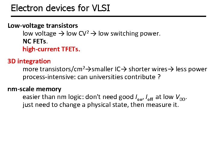
Electron devices for VLSI Low-voltage transistors low voltage → low CV 2 → low switching power. NC FETs. high-current TFETs. 3 D integration more transistors/cm 2→smaller IC→ shorter wires→ less power process-intensive: can universities contribute ? nm-scale memory easier than nm logic: don't need good Ion, Ioff at low VDD. just need to change a physical state, then measure it.

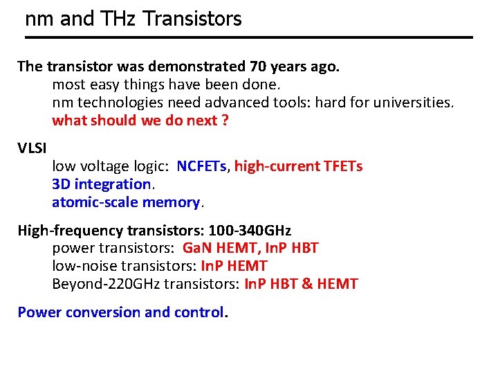
nm and THz Transistors The transistor was demonstrated 70 years ago. most easy things have been done. nm technologies need advanced tools: hard for universities. what should we do next ? VLSI low voltage logic: NCFETs, high-current TFETs 3 D integration. atomic-scale memory. High-frequency transistors: 100 -340 GHz power transistors: Ga. N HEMT, In. P HBT low-noise transistors: In. P HEMT Beyond-220 GHz transistors: In. P HBT & HEMT Power conversion and control.

(backup slides follow)

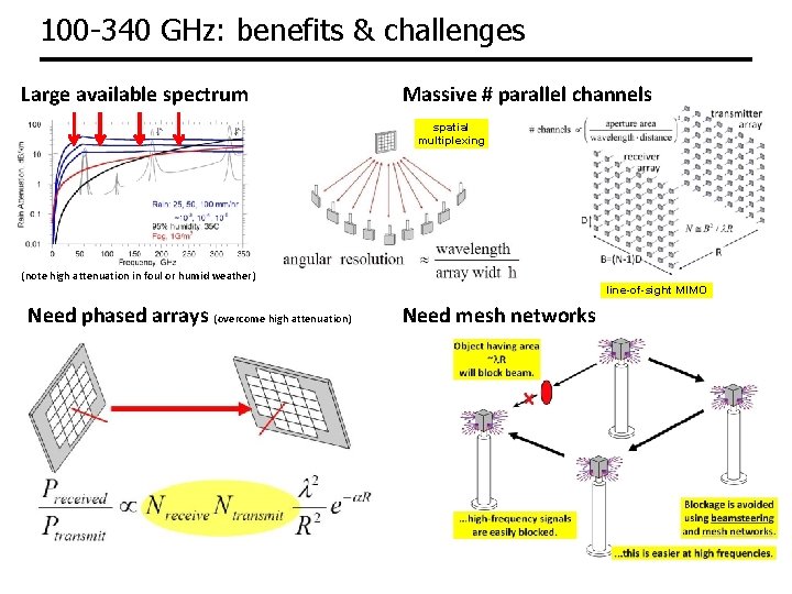
100 -340 GHz: benefits & challenges Large available spectrum Massive # parallel channels spatial multiplexing (note high attenuation in foul or humid weather) line-of-sight MIMO Need phased arrays (overcome high attenuation) Need mesh networks

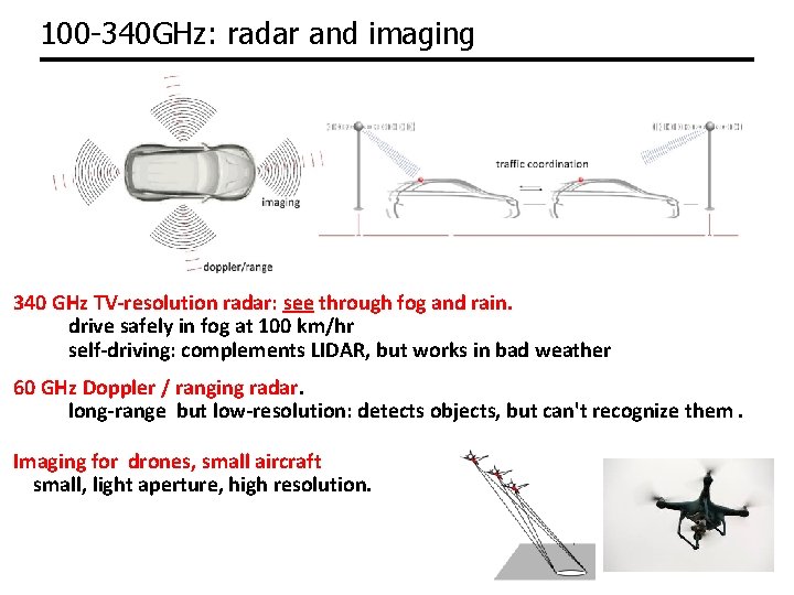
100 -340 GHz: radar and imaging 340 GHz TV-resolution radar: see through fog and rain. drive safely in fog at 100 km/hr self-driving: complements LIDAR, but works in bad weather 60 GHz Doppler / ranging radar. long-range but low-resolution: detects objects, but can't recognize them. Imaging for drones, small aircraft small, light aperture, high resolution.

Effect of order of pad stripping

Effect of order of pad stripping

In. P HBTs: 1. 07 THz @200 nm, ? ? @ 130 nm ? Rode et al. , IEEE TED, Aug. 2015