ENG 2410 Digital Design Week 11 Memory Systems










- Slides: 70

ENG 2410 Digital Design: Week #11 “Memory Systems” S. Areibi School of Engineering University of Guelph

Week #11 Topics o Random Access Memory § § o o Static RAM Array of RAM ICs Dynamic RAM Types of Dynamic RAM Comparison Larger Wider Memories

Resources Chapter #9, Mano Sections l l l 9. 1 9. 2 9. 3 9. 4 9. 5 9. 6 Memory Definitions Random Access Memory SRAM Integrated Circuits Array of SRAM ICs DRAM Types

Computers & Memory

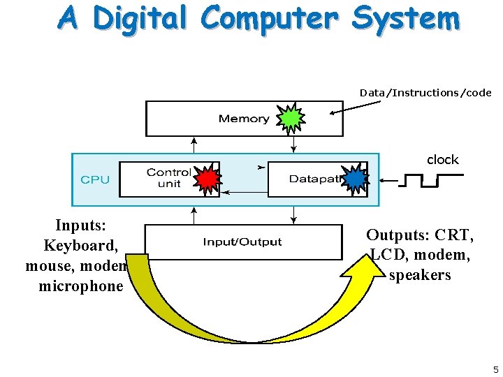
A Digital Computer System Data/Instructions/code clock Inputs: Keyboard, mouse, modem, microphone Outputs: CRT, LCD, modem, speakers 5

Memory: Introduction

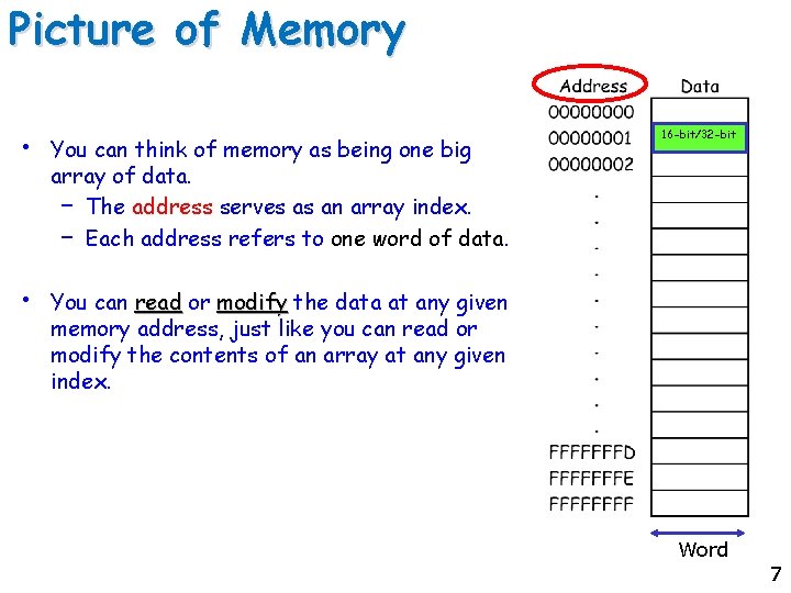
Picture of Memory • You can think of memory as being one big array of data. – The address serves as an array index. – Each address refers to one word of data. • You can read or modify the data at any given memory address, just like you can read or modify the contents of an array at any given index. 16 -bit/32 -bit Word 7

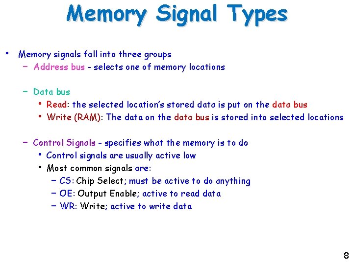
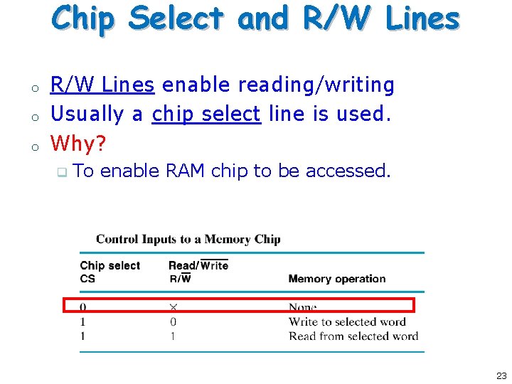
Memory Signal Types • Memory signals fall into three groups – Address bus - selects one of memory locations – Data bus • Read: the selected location’s stored data is put on the data bus • Write (RAM): The data on the data bus is stored into selected locations – Control Signals - specifies what the memory is to do • Control signals are usually active low • Most common signals are: – CS: Chip Select; must be active to do anything – OE: Output Enable; active to read data – WR: Write; active to write data 8

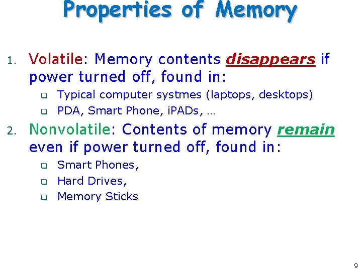
Properties of Memory 1. Volatile: Memory contents disappears if power turned off, found in: q q 2. Typical computer systmes (laptops, desktops) PDA, Smart Phone, i. PADs, … Nonvolatile: Contents of memory remain even if power turned off, found in: q q q Smart Phones, Hard Drives, Memory Sticks 9

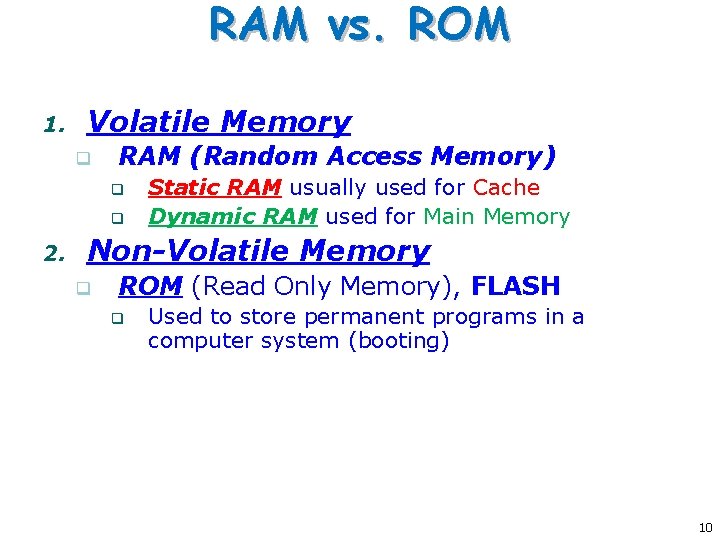
RAM vs. ROM 1. Volatile Memory q RAM (Random Access Memory) q q 2. Static RAM usually used for Cache Dynamic RAM used for Main Memory Non-Volatile Memory q ROM (Read Only Memory), FLASH q Used to store permanent programs in a computer system (booting) 10

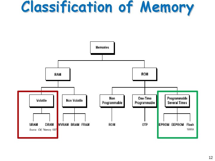
Classification

Classification of Memory 12

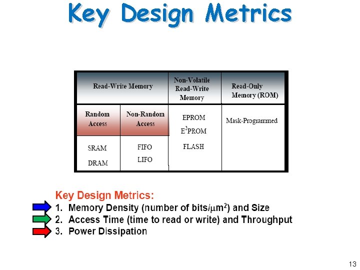
Key Design Metrics 13

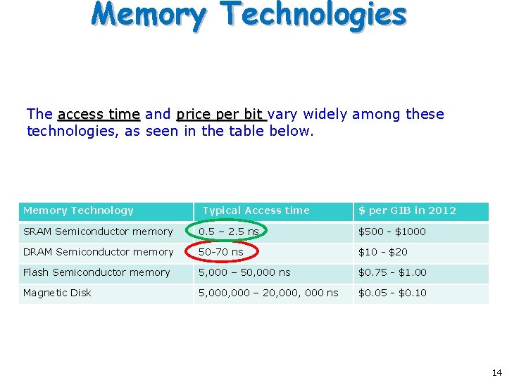
Memory Technologies The access time and price per bit vary widely among these technologies, as seen in the table below. Memory Technology Typical Access time $ per GIB in 2012 SRAM Semiconductor memory 0. 5 – 2. 5 ns $500 - $1000 DRAM Semiconductor memory 50 -70 ns $10 - $20 Flash Semiconductor memory 5, 000 – 50, 000 ns $0. 75 - $1. 00 Magnetic Disk 5, 000 – 20, 000 ns $0. 05 - $0. 10 14

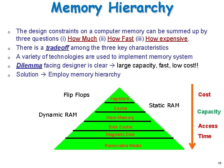
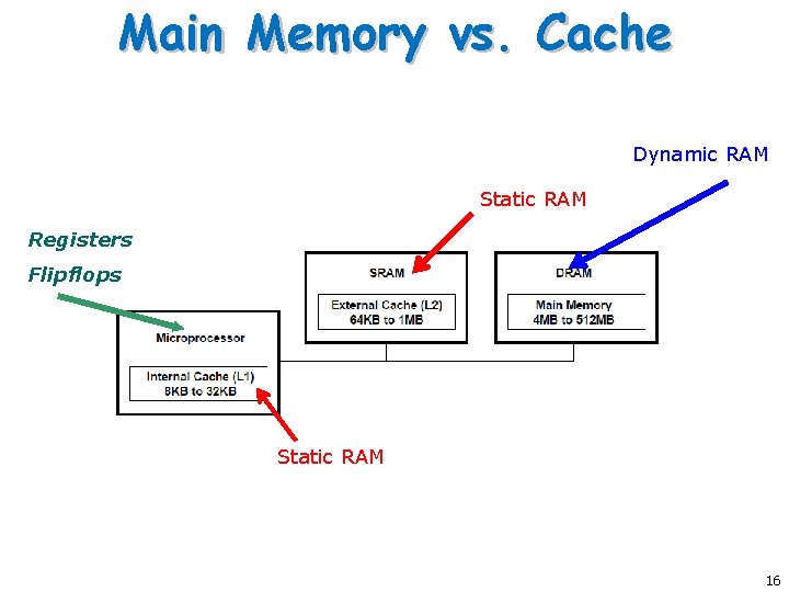
Memory Hierarchy o o o The design constraints on a computer memory can be summed up by three questions (i) How Much (ii) How Fast (iii) How expensive. There is a tradeoff among the three key characteristics A variety of technologies are used to implement memory system Dilemma facing designer is clear large capacity, fast, low cost!! Solution Employ memory hierarchy Flip Flops Cache Dynamic RAM Cost registers Static RAM Capacity Main Memory Disk Cache Magnetic Disk Access Time Removable Media 15

Main Memory vs. Cache Dynamic RAM Static RAM Registers Flipflops Static RAM 16

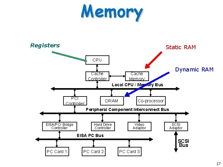
Memory Registers Static RAM CPU Cache Controller PCI Controller Cache Memory Local CPU / Memory Bus DRAM Dynamic RAM Co-processor Peripheral Component Interconnect Bus EISA/PCI Bridge Controller Hard Drive Controller Video Adaptor SCSI Adaptor EISA PC Bus SCSI Bus PC Card 1 PC Card 2 PC Card 3 17

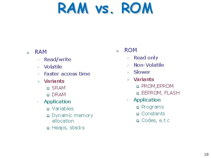
RAM vs. ROM o RAM ü û ü Ø Read/write Volatile Faster access time Variants q q • o q q û ü û Ø SRAM DRAM Application q ROM Variables Dynamic memory allocation Heaps, stacks Read only Non-Volatile Slower Variants q q • PROM, EPROM EEPROM, FLASH Application q q q Programs Constants Codes, e. t. c 18

Random Access Memory

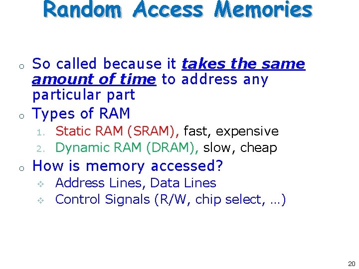
Random Access Memories o o So called because it takes the same amount of time to address any particular part Types of RAM 1. 2. o Static RAM (SRAM), fast, expensive Dynamic RAM (DRAM), slow, cheap How is memory accessed? v v Address Lines, Data Lines Control Signals (R/W, chip select, …) 20

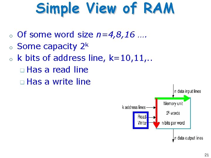
Simple View of RAM o o o Of some word size n=4, 8, 16 …. Some capacity 2 k k bits of address line, k=10, 11, . . q Has a read line q Has a write line 21

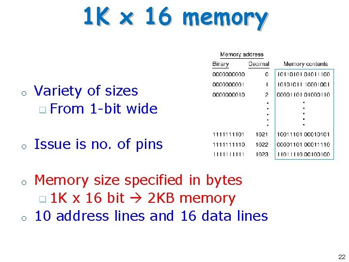
1 K x 16 memory o o Variety of sizes q From 1 -bit wide Issue is no. of pins Memory size specified in bytes q 1 K x 16 bit 2 KB memory 10 address lines and 16 data lines 22

Chip Select and R/W Lines o o o R/W Lines enable reading/writing Usually a chip select line is used. Why? q To enable RAM chip to be accessed. 23

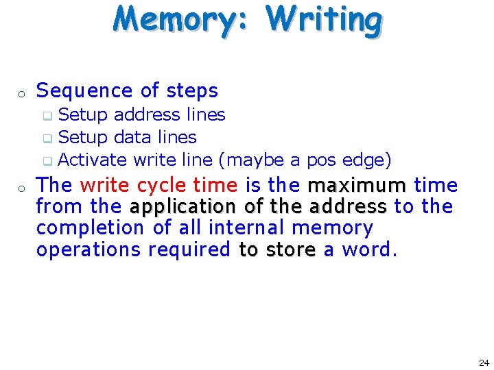
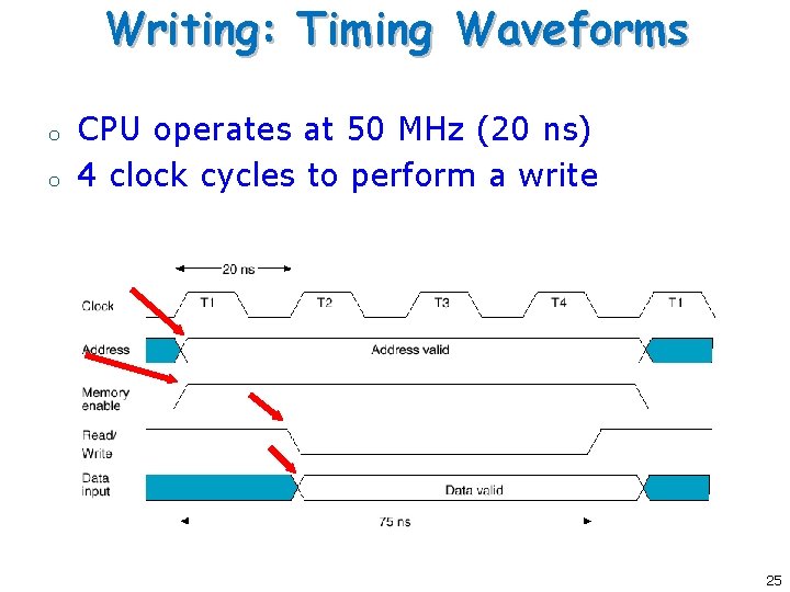
Memory: Writing o Sequence of steps Setup address lines q Setup data lines q Activate write line (maybe a pos edge) q o The write cycle time is the maximum time from the application of the address to the completion of all internal memory operations required to store a word. 24

Writing: Timing Waveforms o o CPU operates at 50 MHz (20 ns) 4 clock cycles to perform a write 25

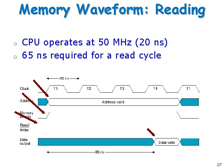
Memory Reading o Steps Setup address lines q Activate read line q Data available after specified amount of time q o Read cycle usually is shorter than write cycle. 26

Memory Waveform: Reading o o CPU operates at 50 MHz (20 ns) 65 ns required for a read cycle 27

Static RAM

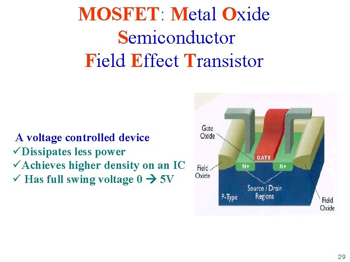
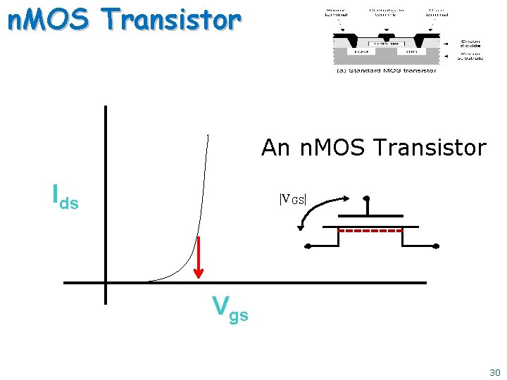
MOSFET: Metal Oxide Semiconductor Field Effect Transistor A voltage controlled device üDissipates less power üAchieves higher density on an IC ü Has full swing voltage 0 5 V 29

n. MOS Transistor An n. MOS Transistor Ids |V GS| Vgs 30

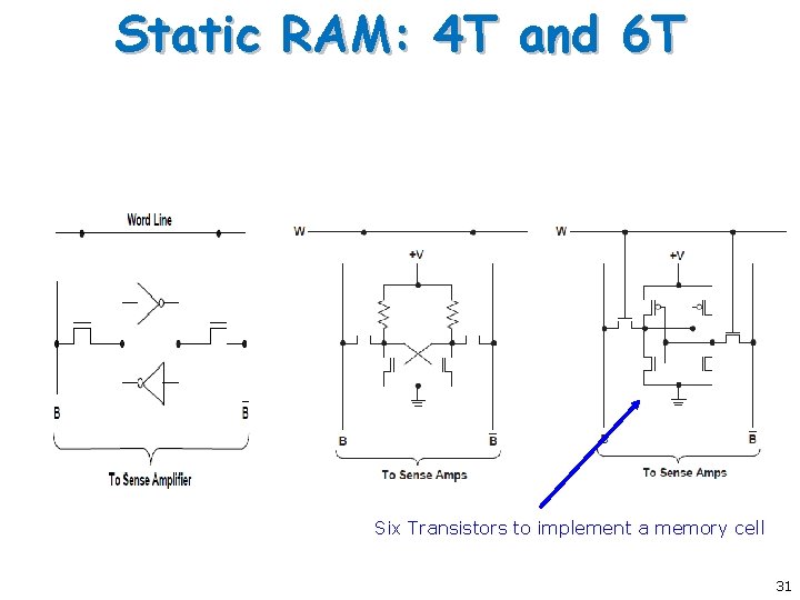
Static RAM: 4 T and 6 T Six Transistors to implement a memory cell 31

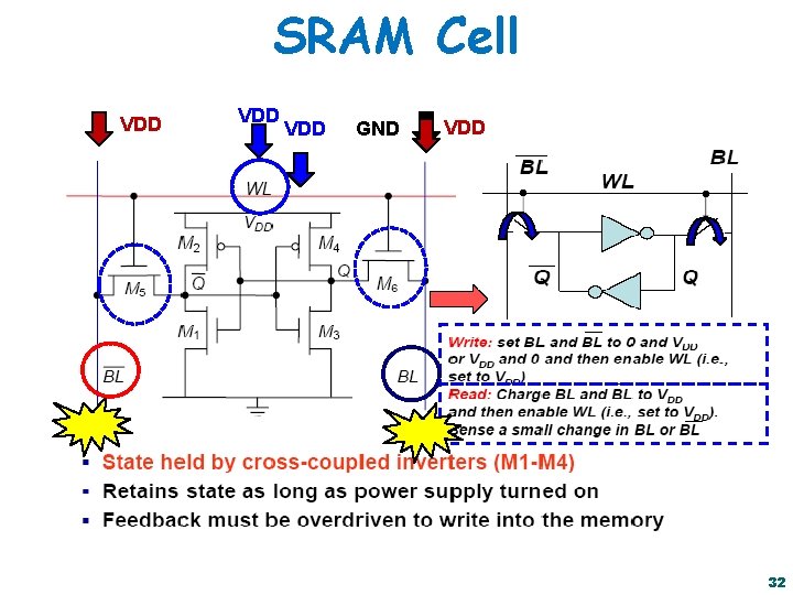
SRAM Cell VDD VDD GND VDD 32

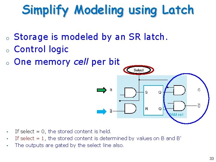
Simplify Modeling using Latch o o o • • • Storage is modeled by an SR latch. Control logic One memory cell per bit If select = 0, the stored content is held. If select = 1, the stored content is determined by values on B and B’ The outputs are gated by the select line also. 33

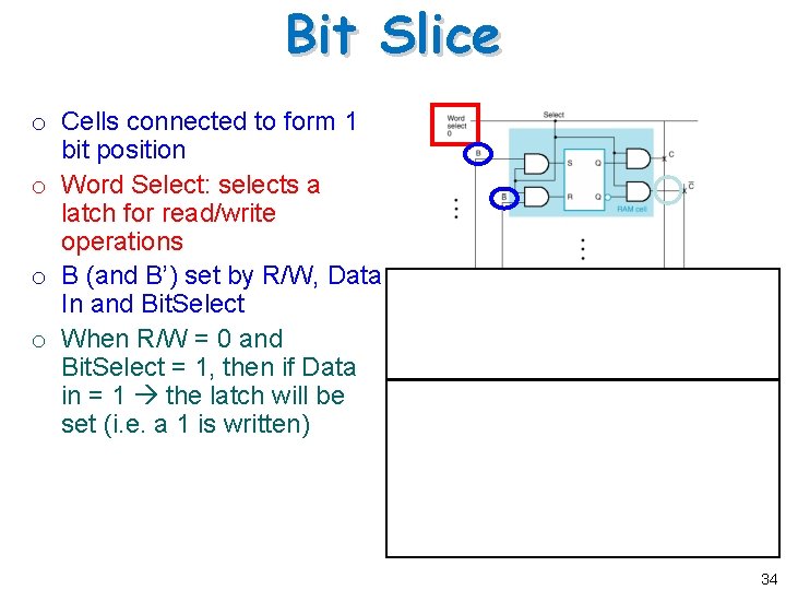
Bit Slice o Cells connected to form 1 bit position o Word Select: selects a latch for read/write operations o B (and B’) set by R/W, Data In and Bit. Select o When R/W = 0 and Bit. Select = 1, then if Data in = 1 the latch will be set (i. e. a 1 is written) 34

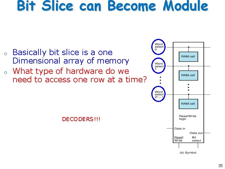
Bit Slice can Become Module o o Basically bit slice is a one Dimensional array of memory What type of hardware do we need to access one row at a time? DECODERS!!! 35

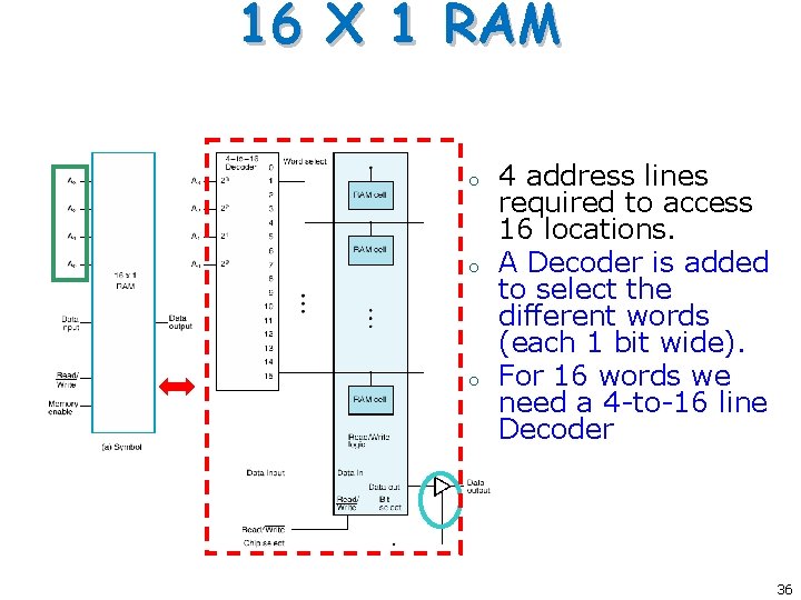
16 X 1 RAM o o o 4 address lines required to access 16 locations. A Decoder is added to select the different words (each 1 bit wide). For 16 words we need a 4 -to-16 line Decoder 36

Row/Column o o Practical memories contains thousands of words!! If RAM gets large, there is a huge decoder Also run into chip layout issues How can we change the structure of Memory to solve this problem? Rearrange the memory into “ 2 D” i. e. , matrix layout 37

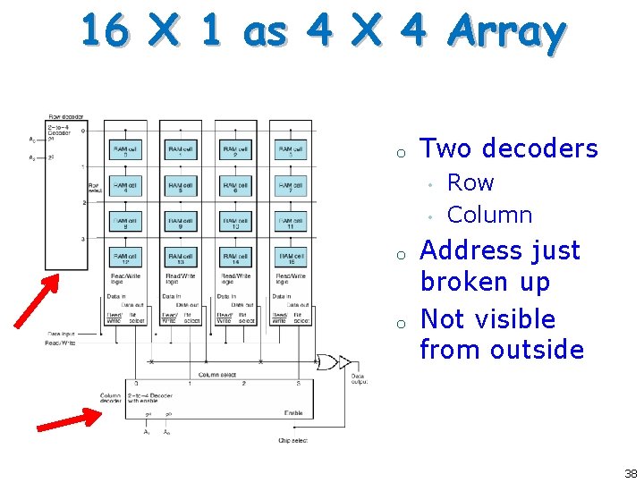
16 X 1 as 4 X 4 Array o Two decoders • • o o Row Column Address just broken up Not visible from outside 38

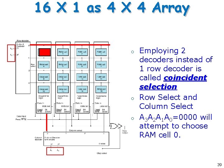
16 X 1 as 4 X 4 Array o o o Employing 2 decoders instead of 1 row decoder is called coincident selection Row Select and Column Select A 3 A 2 A 1 A 0=0000 will attempt to choose RAM cell 0. 39

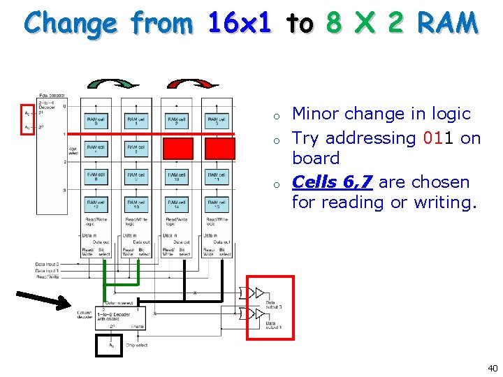
Change from 16 x 1 to 8 X 2 RAM o o o Minor change in logic Try addressing 011 on board Cells 6, 7 are chosen for reading or writing. 40

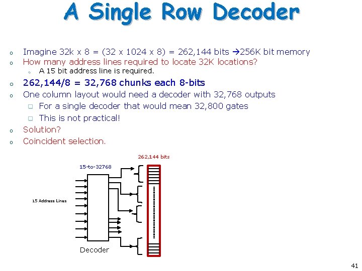
A Single Row Decoder o o Imagine 32 k x 8 = (32 x 1024 x 8) = 262, 144 bits 256 K bit memory How many address lines required to locate 32 K locations? o o o A 15 bit address line is required. 262, 144/8 = 32, 768 chunks each 8 -bits One column layout would need a decoder with 32, 768 outputs q For a single decoder that would mean 32, 800 gates q This is not practical! Solution? Coincident selection. 262, 144 bits 15 -to-32768 15 Address Lines Decoder 41

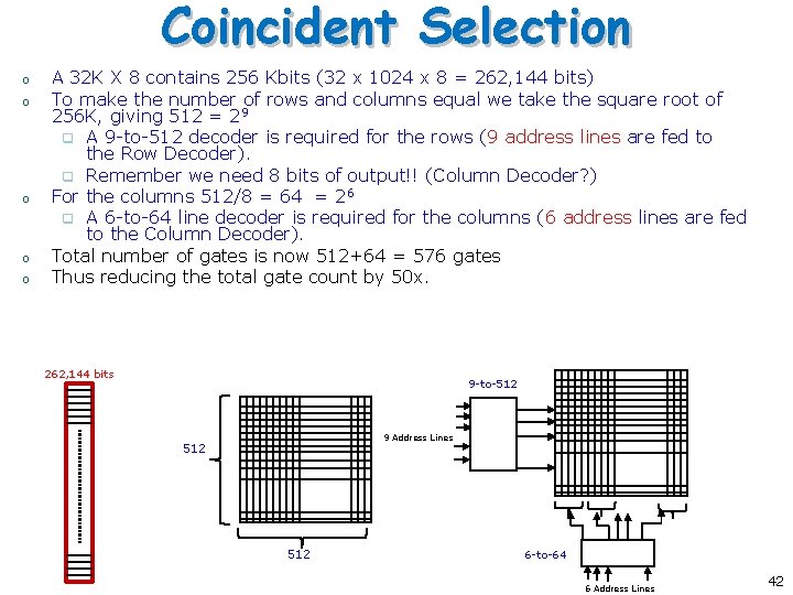
Coincident Selection o o o A 32 K X 8 contains 256 Kbits (32 x 1024 x 8 = 262, 144 bits) To make the number of rows and columns equal we take the square root of 256 K, giving 512 = 29 q A 9 -to-512 decoder is required for the rows (9 address lines are fed to the Row Decoder). q Remember we need 8 bits of output!! (Column Decoder? ) For the columns 512/8 = 64 = 26 q A 6 -to-64 line decoder is required for the columns (6 address lines are fed to the Column Decoder). Total number of gates is now 512+64 = 576 gates Thus reducing the total gate count by 50 x. 262, 144 bits 9 -to-512 9 Address Lines 512 6 -to-64 6 Address Lines 42

SRAM Performance o o o Current SRAMs have cycle times in low nanoseconds (say 2. 5 ns) Used as cache (typically on-chip or offchip secondary cache) Sizes up to 256 Mbit or so for fast chips 43

Memory Expansion

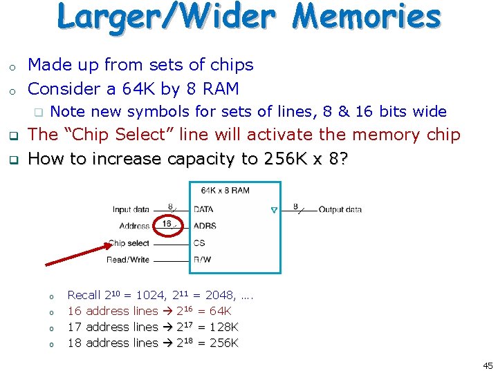
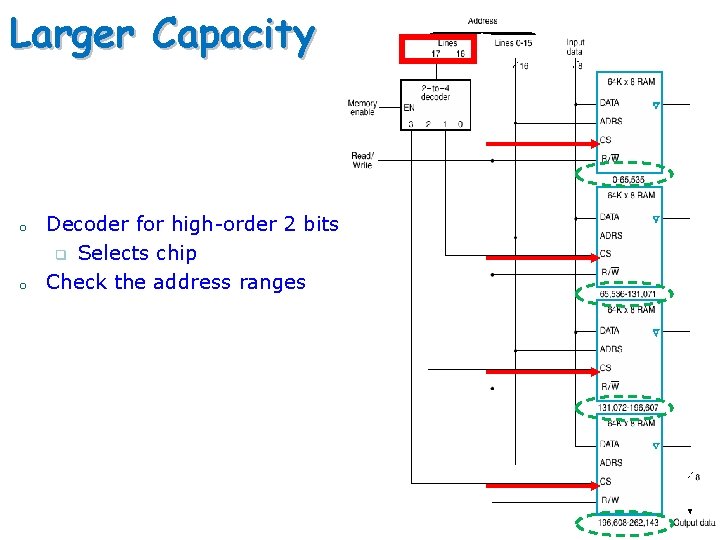
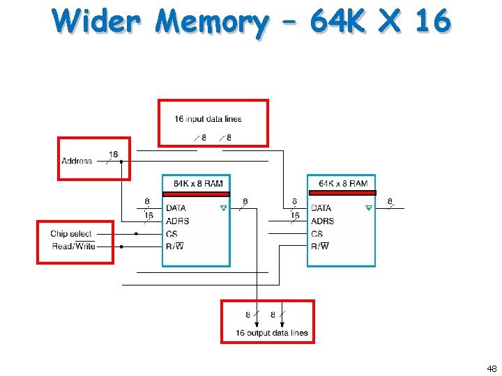
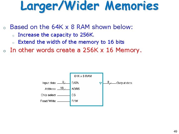
Larger/Wider Memories o o Made up from sets of chips Consider a 64 K by 8 RAM q q q Note new symbols for sets of lines, 8 & 16 bits wide The “Chip Select” line will activate the memory chip How to increase capacity to 256 K x 8? o o Recall 210 = 1024, 211 = 2048, …. 16 address lines 216 = 64 K 17 address lines 217 = 128 K 18 address lines 218 = 256 K 45

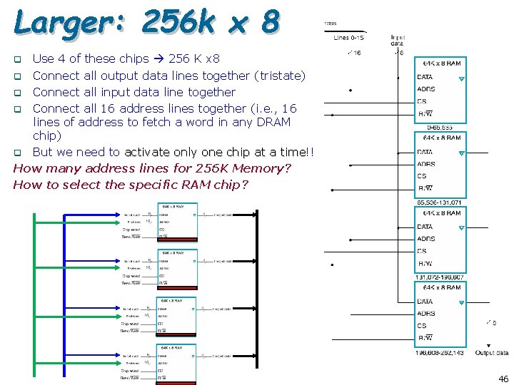
Larger: 256 k x 8 Use 4 of these chips 256 K x 8 q Connect all output data lines together (tristate) q Connect all input data line together q Connect all 16 address lines together (i. e. , 16 lines of address to fetch a word in any DRAM chip) q But we need to activate only one chip at a time!! time How many address lines for 256 K Memory? How to select the specific RAM chip? q 46

Larger Capacity o o Decoder for high-order 2 bits q Selects chip Check the address ranges 47

Wider Memory – 64 K X 16 48

Larger/Wider Memories o Based on the 64 K x 8 RAM shown below: o o o Increase the capacity to 256 K. Extend the width of the memory to 16 bits In other words create a 256 K x 16 Memory. 49

Dynamic RAM

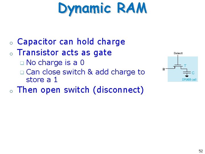
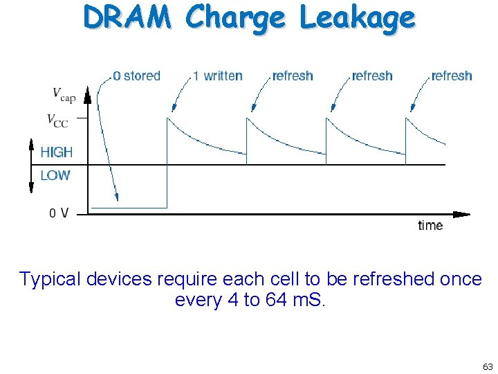
Dynamic Memory • Dynamic memory is built with capacitors. – A stored charge on the capacitor represents a logical 1. – No charge represents a logic 0. • However, capacitors lose their charge after a few milliseconds. The memory requires constant refreshing to recharge the capacitors. (That’s what’s “dynamic” about it. ) • Dynamic RAMs tend to be physically smaller than static RAMs. – A single bit of data can be stored with just one capacitor and one transistor, while static RAM cells typically require 4 -6 transistors. – This means dynamic RAM is cheaper and denser—more bits can be stored in the same physical area. 51

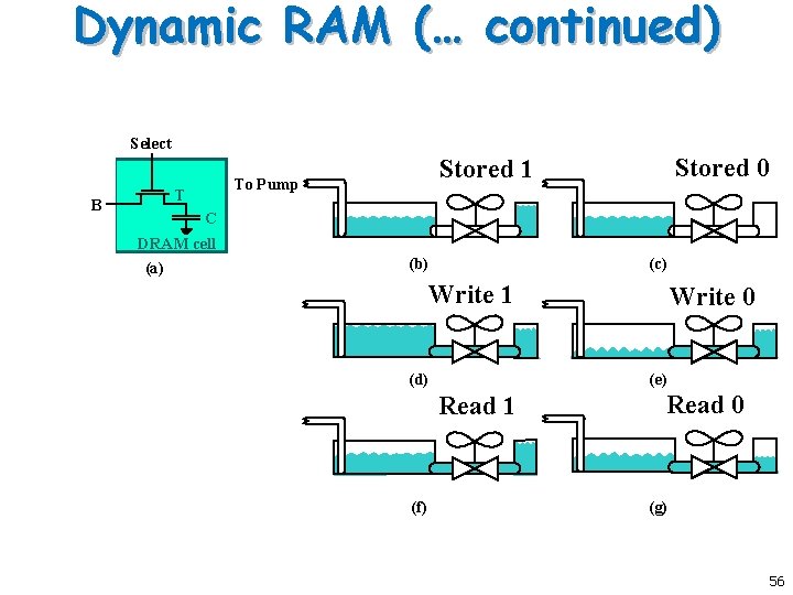
Dynamic RAM o o Capacitor can hold charge Transistor acts as gate No charge is a 0 q Can close switch & add charge to store a 1 q o Then open switch (disconnect) 52

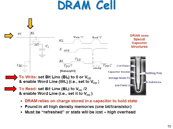
DRAM Cell 53

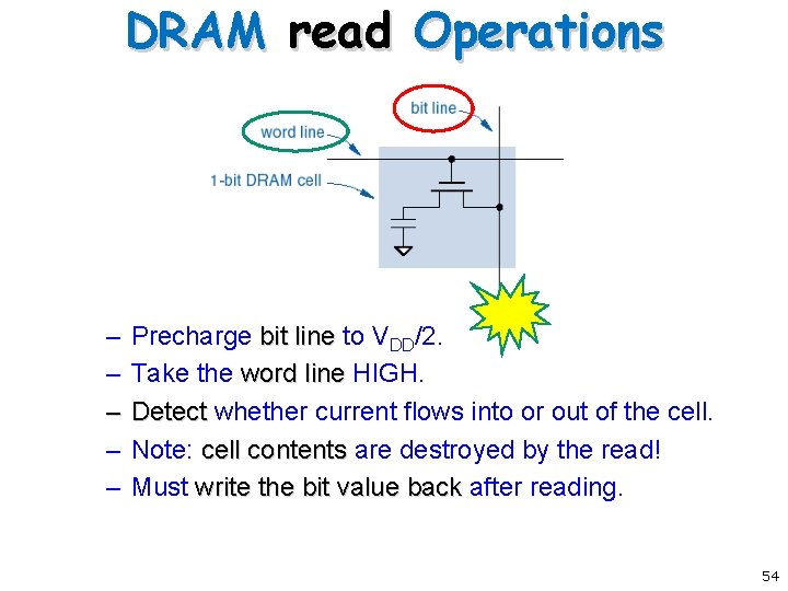
DRAM read Operations – – – Precharge bit line to VDD/2. Take the word line HIGH. Detect whether current flows into or out of the cell. Note: cell contents are destroyed by the read! Must write the bit value back after reading. 54

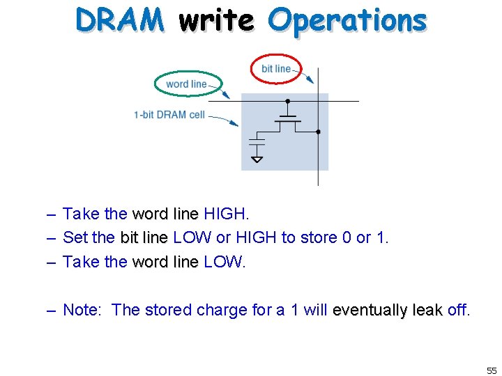
DRAM write Operations – Take the word line HIGH. – Set the bit line LOW or HIGH to store 0 or 1. – Take the word line LOW. – Note: The stored charge for a 1 will eventually leak off. 55

Dynamic RAM (… continued) Select B T Stored 0 Stored 1 To Pump C DRAM cell (a) (b) (c) Write 1 (d) (e) Read 1 (f) Write 0 Read 0 (g) 56

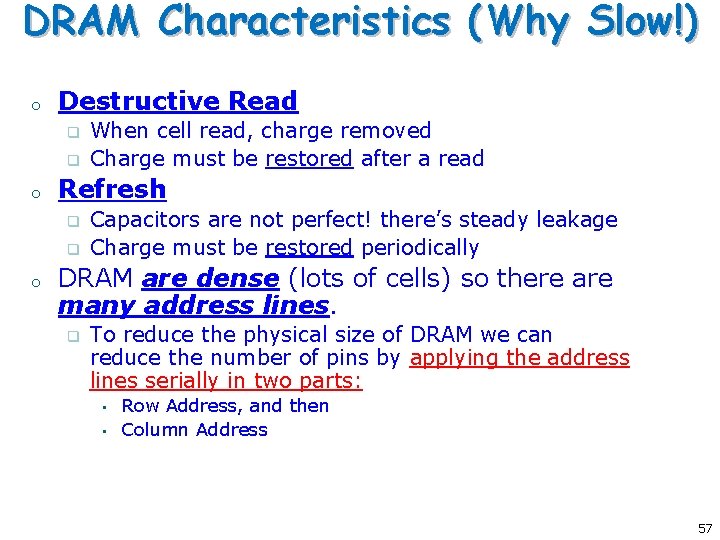
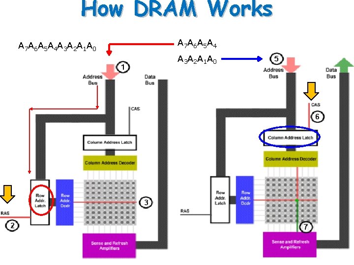
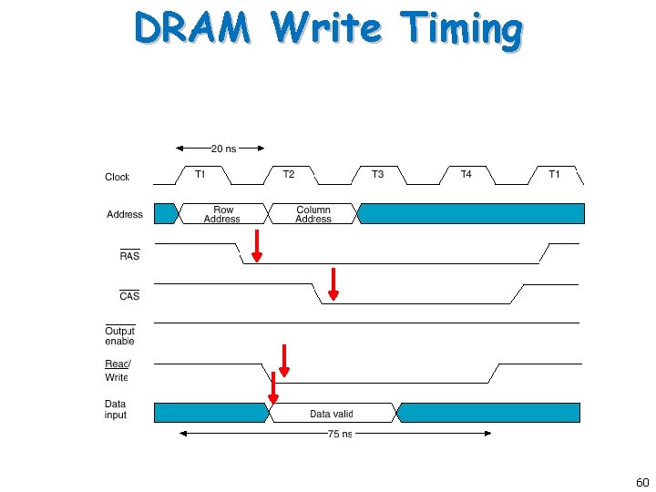
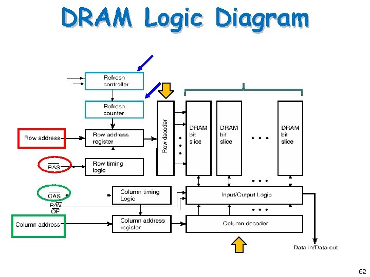
DRAM Characteristics (Why Slow!) o Destructive Read q q o Refresh q q o When cell read, charge removed Charge must be restored after a read Capacitors are not perfect! there’s steady leakage Charge must be restored periodically DRAM are dense (lots of cells) so there are many address lines. q To reduce the physical size of DRAM we can reduce the number of pins by applying the address lines serially in two parts: • • Row Address, and then Column Address 57

How DRAM Works A 7 A 6 A 5 A 4 A 3 A 2 A 1 A 0 A 7 A 6 A 5 A 4 A 3 A 2 A 1 A 0 58

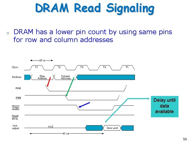
DRAM Read Signaling o DRAM has a lower pin count by using same pins for row and column addresses Delay until data available 59

DRAM Write Timing 60

DRAM Logic Diagram 62

DRAM Charge Leakage Typical devices require each cell to be refreshed once every 4 to 64 m. S. 63

Synchronous DRAM

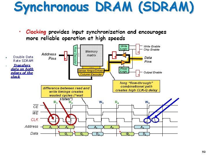
Synchronous DRAM (SDRAM) o o Double Data Rate SDRAM Transfers data on both edges of the clock 69

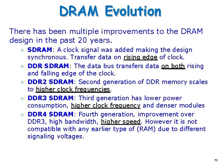
DRAM Evolution There has been multiple improvements to the DRAM design in the past 20 years. v v v SDRAM: A clock signal was added making the design synchronous. Transfer data on rising edge of clock. DDR SDRAM: The data bus transfers data on both rising and falling edge of the clock. DDR 2 SDRAM: Second generation of DDR memory scales to higher clock frequencies DDR 3 SDRAM: Third generation has lower power consumption, higher clock frequency and denser modules DDR 4 SDRAM: Fourth generation, improvement over DDR 3, high bandwidth, higher speed However it is not compatible with any earlier type of (RAM) due to different signaling voltages. 70

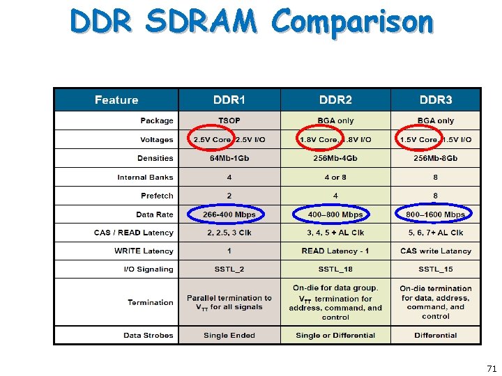
DDR SDRAM Comparison 71

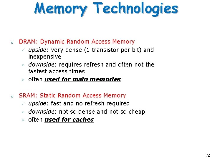
Memory Technologies o o DRAM: Dynamic Random Access Memory ü upside: very dense (1 transistor per bit) and inexpensive û downside: requires refresh and often not the fastest access times Ø often used for main memories SRAM: Static Random Access Memory ü upside: fast and no refresh required û downside: not so dense and not so cheap Ø often used for caches 72

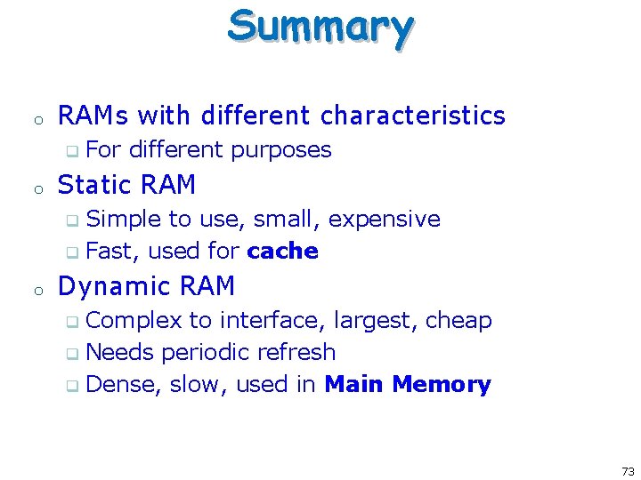
Summary o RAMs with different characteristics q o For different purposes Static RAM Simple to use, small, expensive q Fast, used for cache q o Dynamic RAM Complex to interface, largest, cheap q Needs periodic refresh q Dense, slow, used in Main Memory q 73

Links Ram Guides (not very technical) § http: //arstechnica. com/paedia/storage. html 74
