
ENG 2410 Digital Design Week 8 Registers Counters












- Slides: 51
ENG 2410 Digital Design: Week #8 “Registers & Counters” S. Areibi School of Engineering University of Guelph
Week #8 Topics o o o Definition of Register and Counter Registers, Shift Registers Ripple Counters Synchronous Binary Counters BCD Counters
Resources Chapter #7, Mano Sections l l 7. 1 7. 6 Registers and Load Enable Shift Registers Ripple Counters Synchronous Binary Counters
Registers
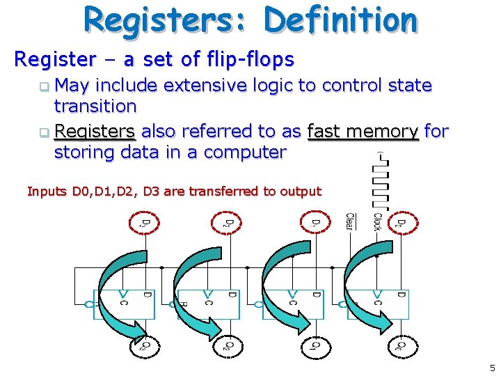
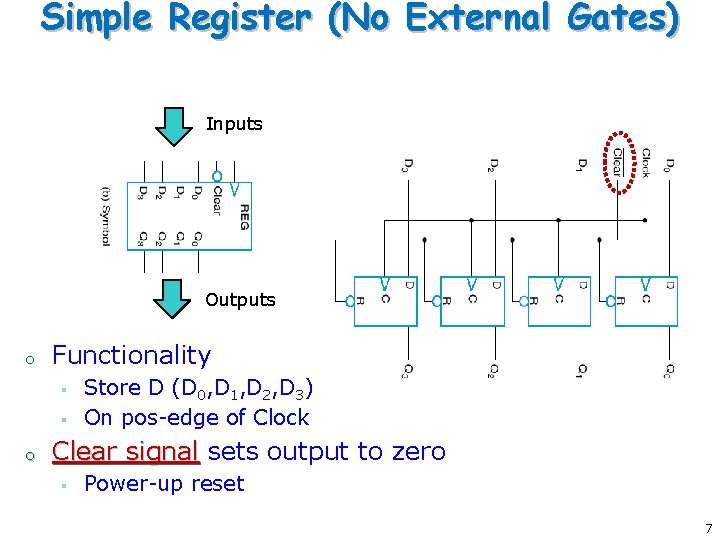
Registers: Definition Register – a set of flip-flops May include extensive logic to control state transition q Registers also referred to as fast memory for storing data in a computer q Inputs D 0, D 1, D 2, D 3 are transferred to output 5
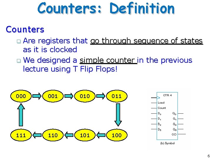
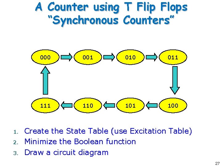
Counters: Definition Counters Are registers that go through sequence of states as it is clocked q We designed a simple counter in the previous lecture using T Flip Flops! q 000 001 010 011 110 101 100 6
Simple Register (No External Gates) Inputs Outputs o Functionality § § o Store D (D 0, D 1, D 2, D 3) On pos-edge of Clock Clear signal sets output to zero § Power-up reset 7
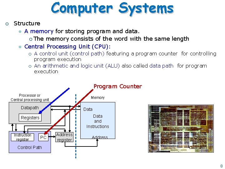
Computer Systems ¡ Structure l A memory for storing program and data. ¡ The memory consists of the word with the same length l Central Processing Unit (CPU): ¡ ¡ A control unit (control path) featuring a program counter for controlling program execution An arithmetic and logic unit (ALU) also called data path for program execution Program Counter Processor or Central processing unit Memory Datapath Data and Instructions Registers Instruction register PC Address register Address Control Path 8
Disabling the Clocking
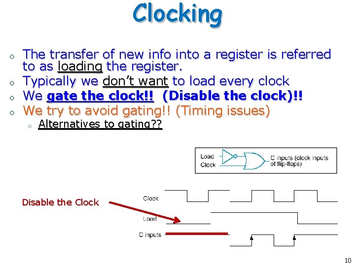
Clocking o o The transfer of new info into a register is referred to as loading the register. Typically we don’t want to load every clock We gate the clock!! (Disable the clock)!! We try to avoid gating!! (Timing issues) o Alternatives to gating? ? Disable the Clock 10
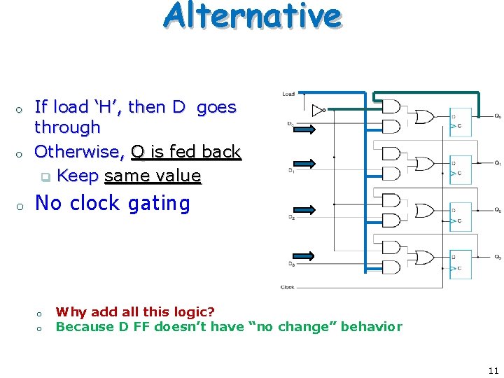
Alternative o o o If load ‘H’, then D goes through Otherwise, Q is fed back q Keep same value No clock gating o o Why add all this logic? Because D FF doesn’t have “no change” behavior 11
Shift Registers
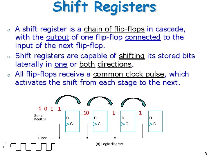
Shift Registers o o o A shift register is a chain of flip-flops in cascade, with the output of one flip-flop connected to the input of the next flip-flop. Shift registers are capable of shifting its stored bits laterally in one or both directions. All flip-flops receive a common clock pulse, which activates the shift from each stage to the next. 1 0 1 1 13
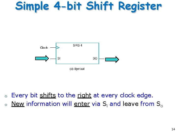
Simple 4 -bit Shift Register o o Every bit shifts to the right at every clock edge. New information will enter via Si and leave from So 14
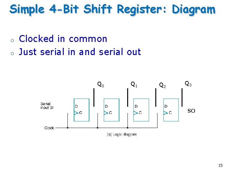
Simple 4 -Bit Shift Register: Diagram o o Clocked in common Just serial in and serial out Q 0 Q 1 Q 2 Q 3 SO 15
VHDL
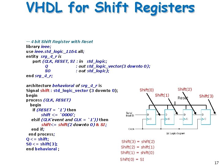
VHDL for Shift Registers -- 4 bit Shift Register with Reset library ieee; use ieee. std_logic_1164. all; entity srg_4_r is port (CLK, RESET, SI : in std_logic; Q : out std_logic_vector(3 downto 0); SO : out std_logic); end srg_4_r; architecture behavioral of srg_4_r is Shift(0) Signal shift : std_logic_vector (3 downto 0); Shift(1) begin process (CLK, RESET) begin if (RESET = `1’) then shift <= `0000’; elsif (CLK’event and CLK = `1’)) then shift<= shift(2 downto 0) & SI; end if; end process; Q <= shift; Shift(3) = shift(2) S 0 <= shift(3); Shift(2) = shift(1) end behavioral ; Shift(1) = shift(0) Shift(0) = SI Shift(2) Reset Shift(3) 17
Registers: Alternative Types
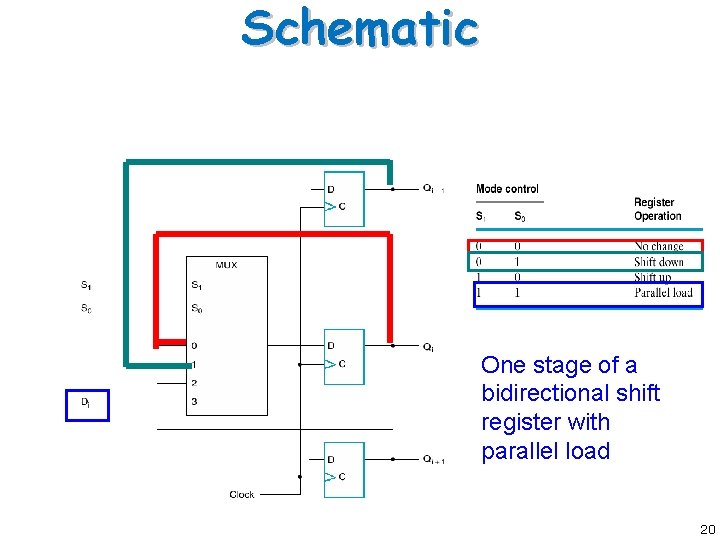
Bidirectional Shift Register o o Shift either way (Left or Right) Now we have following possible inputs Parallel load q Shift from left q Shift from right q Also “no change” q 19
Schematic One stage of a bidirectional shift register with parallel load 20
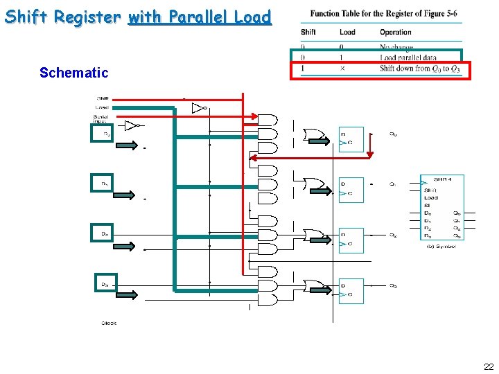
Shift Register with Parallel Load o o Load any value to the shift register The shift register can then shift information one bit at a time 21
Shift Register with Parallel Load Schematic 22
Shift Registers (Summary) o Capability to shift bits q o In one or both directions Usage? Part of standard CPU instruction set q Cheap Multiplication/Division q Serial communications q 23
Synchronous Counters
Counters o o Counter is a register – but has states Also goes through sequence of states – counts – on clock or other pulses Examples: Binary Counter q q o o Counts through binary sequence n bit counter counts from 0 to 2 n – 1 BCD Counter Any Sequence Counter 25
Synthesis Using T Flip Flops o Design a counter that counts from “ 000” to “ 111” and then back to “ 000” again. o Constraint: Use T Flip-Flops Where do we start? Start with a state diagram. 26
A Counter using T Flip Flops “Synchronous Counters” 1. 2. 3. 000 001 010 011 110 101 100 Create the State Table (use Excitation Table) Minimize the Boolean function Draw a circuit diagram 27
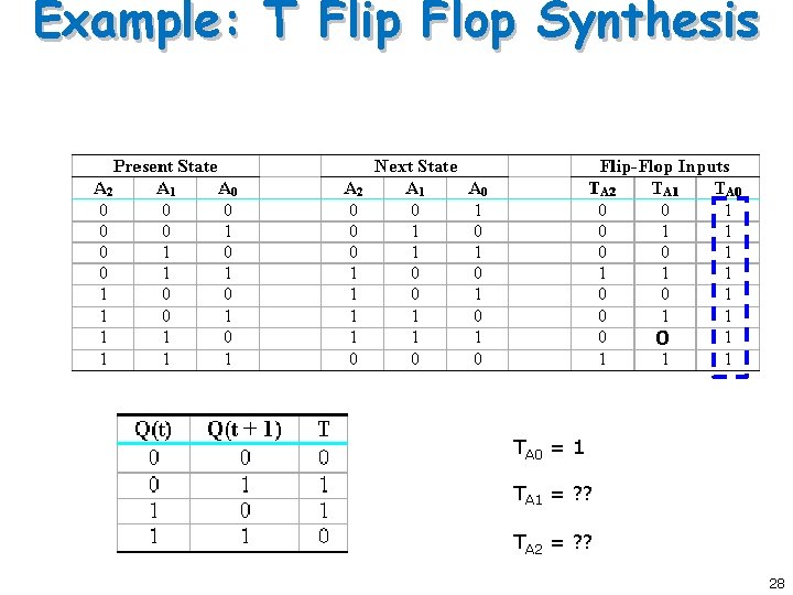
Example: T Flip Flop Synthesis 0 TA 0 = 1 TA 1 = ? ? TA 2 = ? ? 28
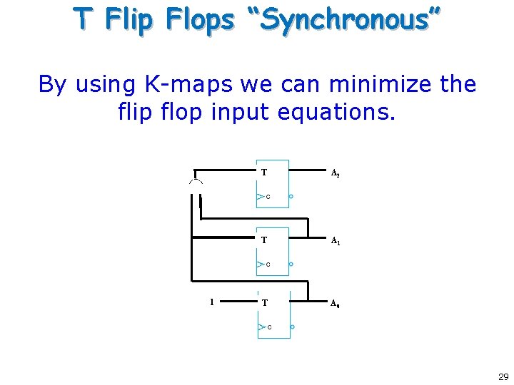
T Flip Flops “Synchronous” By using K-maps we can minimize the flip flop input equations. 1 T A 2 T A 1 T A 0 29
Asynchronous Counters
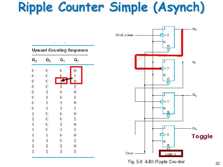
Asynchronous Counters Asynchronous counters are yet another type of counters where not all flip flops are driven by the global clock. ¡ Ripple counters are asynchronous counters that are easy to design. ¡ 31
Ripple Counter Simple (Asynch) Toggle 32
Counters with Parallel Load
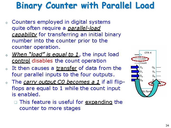
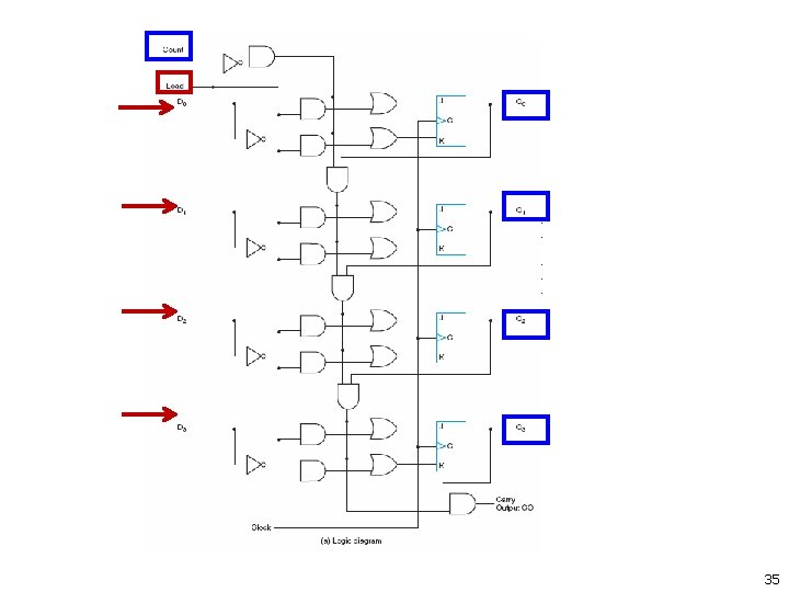
Binary Counter with Parallel Load o o Counters employed in digital systems quite often require a parallel-load capability for transferring an initial binary number into the counter prior to the counter operation. When “load” is equal to 1, 1 the input load control disables the count operation It then causes a transfer of data from the four parallel inputs to the four outputs. The carry output C 0 becomes a 1 if all flipflops are equal to 1 while the count input is enabled. q This feature is useful for expanding the counter to more stages 34
35
BCD Counters
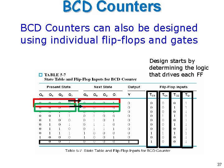
BCD Counters can also be designed using individual flip-flops and gates Design starts by determining the logic that drives each FF 37
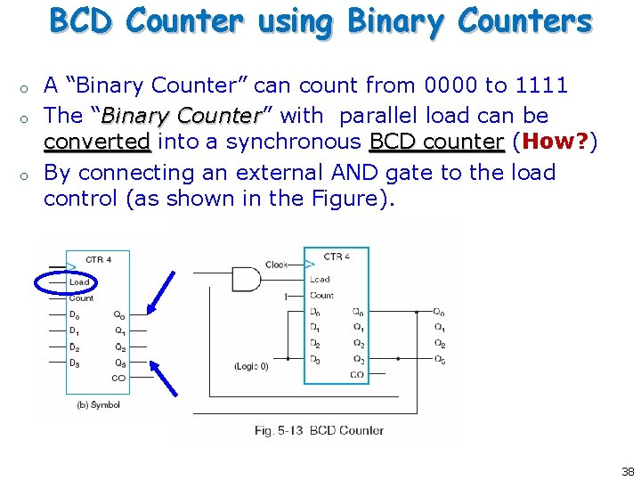
BCD Counter using Binary Counters o o o A “Binary Counter” can count from 0000 to 1111 The “Binary Counter” Counter with parallel load can be converted into a synchronous BCD counter (How? ) By connecting an external AND gate to the load control (as shown in the Figure). 38
Arbitrary Counters
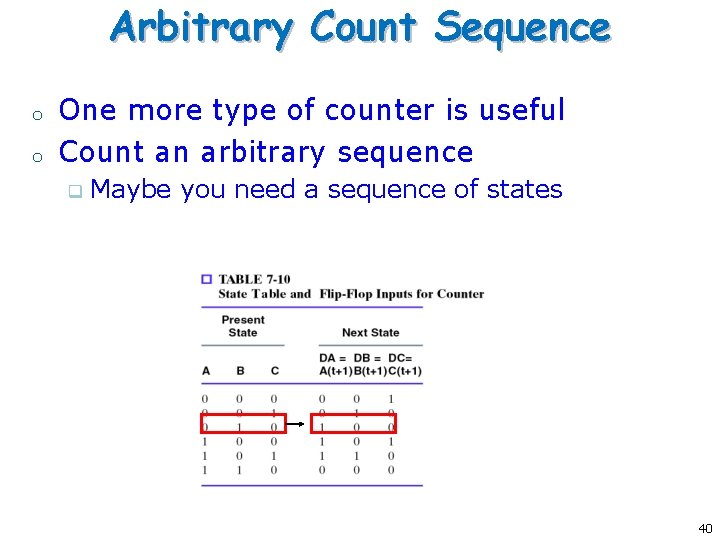
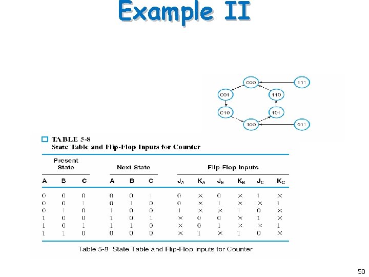
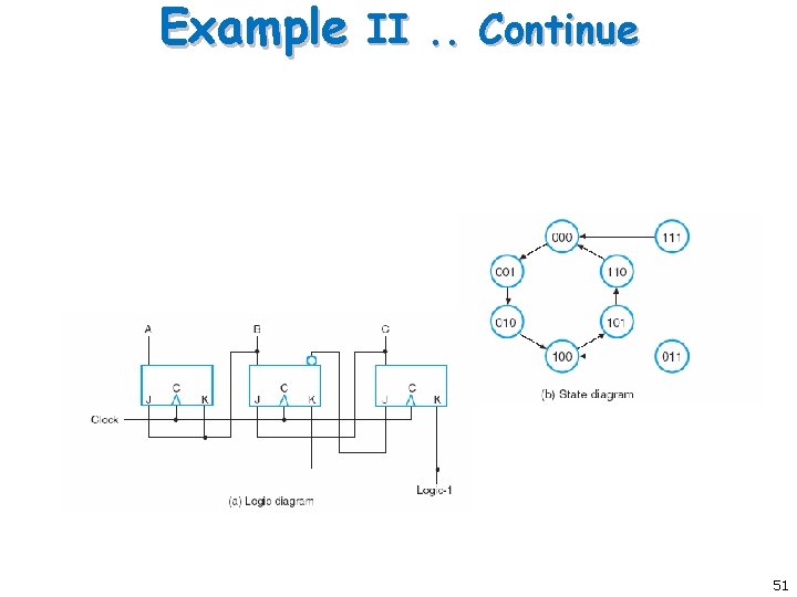
Arbitrary Count Sequence o o One more type of counter is useful Count an arbitrary sequence q Maybe you need a sequence of states 40
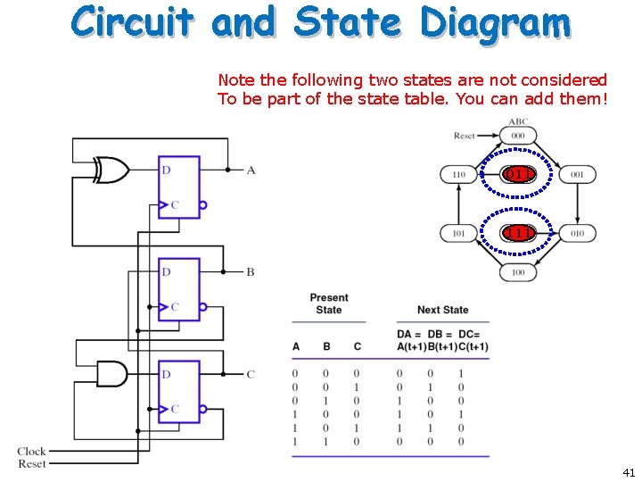
Circuit and State Diagram Note the following two states are not considered To be part of the state table. You can add them! 011 111 41
VHDL for Counters
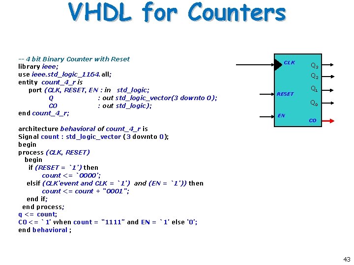
VHDL for Counters -- 4 bit Binary Counter with Reset library ieee; use ieee. std_logic_1164. all; entity count_4_r is port (CLK, RESET, EN : in std_logic; Q : out std_logic_vector(3 downto 0); CO : out std_logic); end count_4_r; CLK Q 3 Q 2 RESET Q 1 Q 0 EN CO architecture behavioral of count_4_r is Signal count : std_logic_vector (3 downto 0); begin process (CLK, RESET) begin if (RESET = `1’) then count <= `0000’; elsif (CLK’event and CLK = `1’) and (EN = `1’)) then count <= count + “ 0001”; end if; end process; q <= count; C 0 <= `1’ when count = “ 1111” and EN = `1’ else ‘ 0’; end behavioral ; 43
Applications: Serial Addition
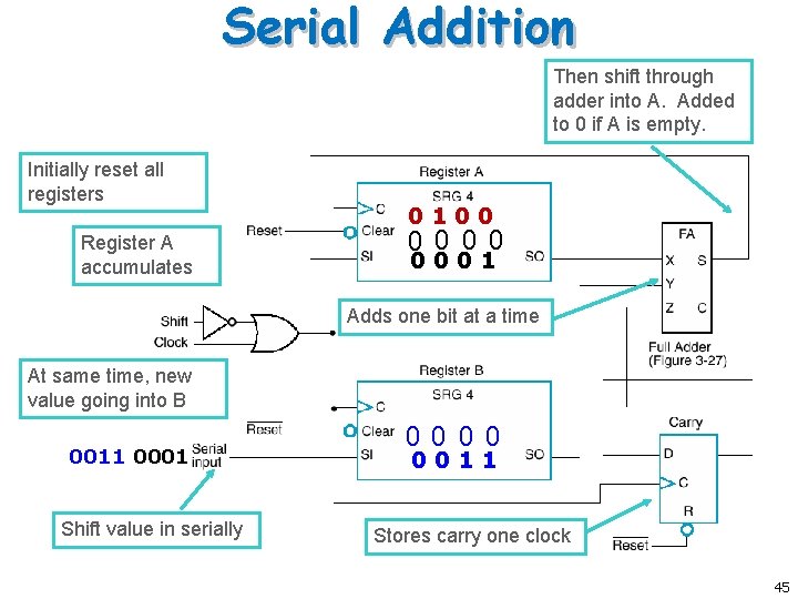
Serial Addition Then shift through adder into A. Added to 0 if A is empty. Initially reset all registers Register A accumulates 0100 0001 Adds one bit at a time At same time, new value going into B 0011 0001 Shift value in serially 0000 0011 Stores carry one clock 45
Hardware Comparison o Serial vs. parallel adder One full adder vs. n full adders q Serial takes n clock cycles, parallel only one clock cycle q o To reduce the amount of hardware to be mapped onto an FPGA designers seek to use alternative solutions: Serial Implementations. q Semi Parallel Implementations q Fully Parallel Implementations. q 46
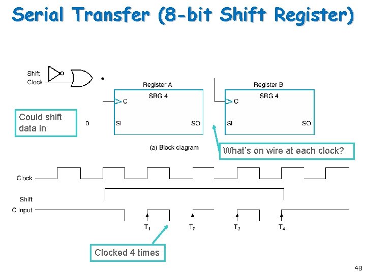
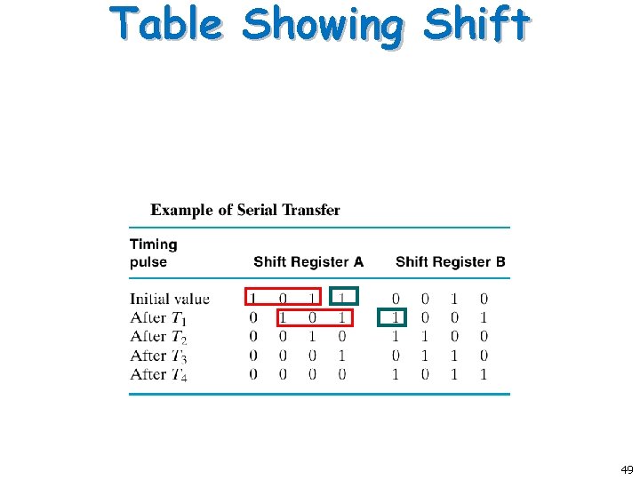
Serial Transfer (8 -bit Shift Register) Could shift data in What’s on wire at each clock? Clocked 4 times 48
Table Showing Shift 49
Example II 50
Example II. . Continue 51