ENG 2410 Digital Design Week 10 Sequencing and











- Slides: 61
ENG 2410 Digital Design: Week #10 “Sequencing and Control” S. Areibi School of Engineering University of Guelph
Week #10 Topics o o The Control Unit Algorithmic State Machines ASM Elements Hardwired Control I. II. o One Flip-Flop Per State Sequence Register and Decoder VHDL Representation
Resources Chapter #8, Mano Sections l l 8. 1 8. 2 8. 3 8. 4 The Control Unit Algorithmic State Machines ASM Examples Hardwired Control
CPU: Control Units
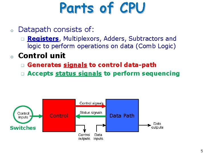
Parts of CPU o Datapath consists of: q o Registers, Multiplexors, Adders, Subtractors and logic to perform operations on data (Comb Logic) Control unit q q Generates signals to control data-path Accepts status signals to perform sequencing Control Data Path Switches 5
The Control Unit The binary information stored in a digital computer can be classified as either data or control information. 1. Data is manipulated in a data-path q q 2. To perform arithmetic, logic, shifting, and other dataprocessing tasks. These operations are implemented with ALUs, registers, multiplexers, and busses. The control unit q q Provides signals that activate the various microoperations in the data-path to perform the specified data processing tasks. The control unit also determines the sequence in which the various actions are performed (i. e. when they are to be performed) 6
Control Unit Types ¡ Two distinct classes: l Programmable l Non-programmable. ¡ A programmable control unit has: l An external ROM or RAM array for storing instructions and control information l A program counter (PC) or other sequencing register with contents that points to the next instruction to be executed l Decision logic for determining the sequence of operations and logic to interpret the instructions ¡ A non-programmable control unit (hardwired Control) does not fetch instructions from a memory but just determines the operations to be performed and the sequence of those operations based only on inputs and status bits. ¡ We will only cover non-programmable control unit 7
Algorithmic State Machines
Algorithmic State Machines (ASM) o o The function of a state machine (or sequential circuit) can be represented by a state table or a state diagram. What is wrong with state diagrams? o o Gets messy as states grow Decisions to move to different states is not present. Solution? A flowchart is a way of showing actions and control flow in an algorithm. q An Algorithmic State Machine (ASM) is simply a flowchart-like way to specify state diagrams for sequential logic and, optionally, actions performed in a datapath. q While flowcharts typically do not specify “time”, an ASM explicitly specifies a sequence of actions and their timing relationships. 9
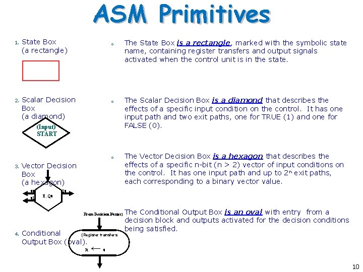
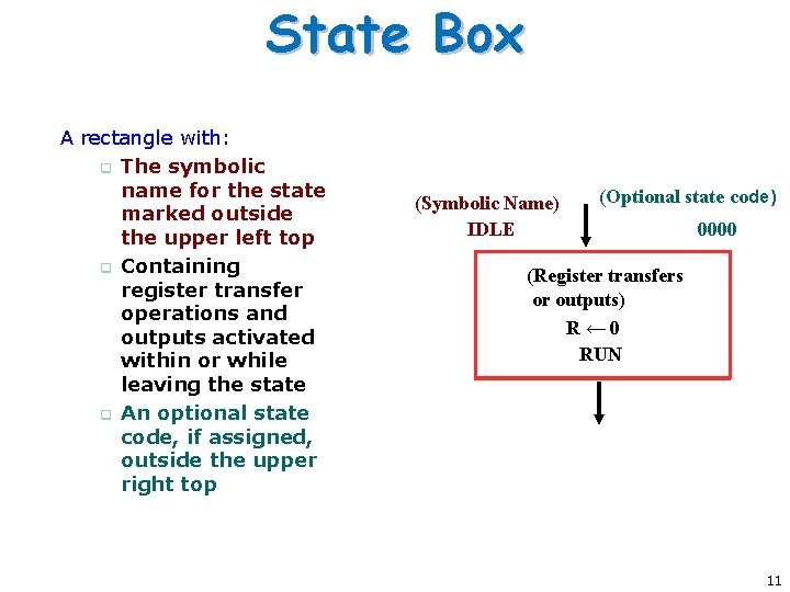
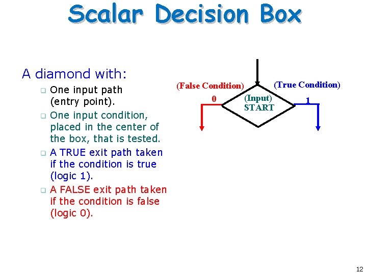
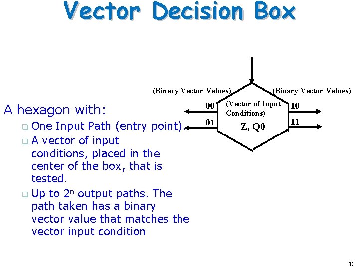
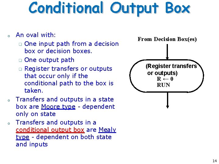
ASM Primitives 1. State Box (a rectangle) 2. Scalar Decision Box (a diamond) o o (Input) START o 3. Vector Decision Box (a hexagon) 00 01 The Scalar Decision Box is a diamond that describes the effects of a specific input condition on the control. It has one input path and two exit paths, one for TRUE (1) and one for FALSE (0). The Vector Decision Box is a hexagon that describes the effects of a specific n-bit (n > 2) vector of input conditions on the control. It has one input path and up to 2 n exit paths, each corresponding to a binary vector value. 10 Z, Q 0 o From Decision Box(es) 4. The State Box is a rectangle, marked with the symbolic state name, containing register transfers and output signals activated when the control unit is in the state. Conditional (Register transfers Output Box (oval). R ← The Conditional Output Box is an oval with entry from a decision block and outputs activated for the decision conditions being satisfied. 0 10
State Box A rectangle with: q The symbolic name for the state marked outside the upper left top q Containing register transfer operations and outputs activated within or while leaving the state q An optional state code, if assigned, outside the upper right top (Symbolic Name) IDLE (Optional state code) 0000 (Register transfers or outputs) R← 0 RUN 11
Scalar Decision Box A diamond with: q q One input path (entry point). One input condition, placed in the center of the box, that is tested. A TRUE exit path taken if the condition is true (logic 1). A FALSE exit path taken if the condition is false (logic 0). (True Condition) (False Condition) (Input) 0 1 START 12
Vector Decision Box (Binary Vector Values) A hexagon with: One Input Path (entry point). q A vector of input conditions, placed in the center of the box, that is tested. q Up to 2 n output paths. The path taken has a binary vector value that matches the vector input condition q 00 01 (Binary Vector Values) (Vector of Input Conditions) Z, Q 0 10 11 13
Conditional Output Box o o o An oval with: q One input path from a decision box or decision boxes. q One output path q Register transfers or outputs that occur only if the conditional path to the box is taken. Transfers and outputs in a state box are Moore type - dependent only on state Transfers and outputs in a conditional output box are Mealy type - dependent on both state and inputs From Decision Box(es) (Register transfers or outputs) R← 0 RUN 14
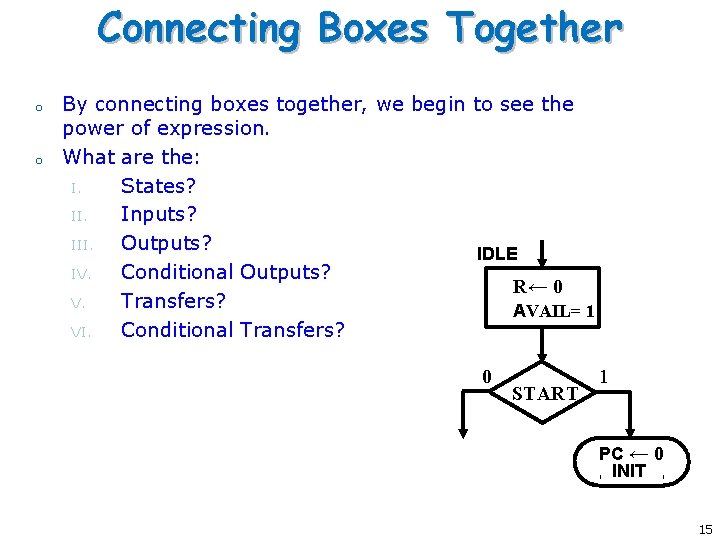
Connecting Boxes Together o o By connecting boxes together, we begin to see the power of expression. What are the: I. States? II. Inputs? III. Outputs? IDLE IV. Conditional Outputs? R← 0 V. Transfers? AVAIL= 1 VI. Conditional Transfers? 0 START 1 PC ← 0 INIT 15
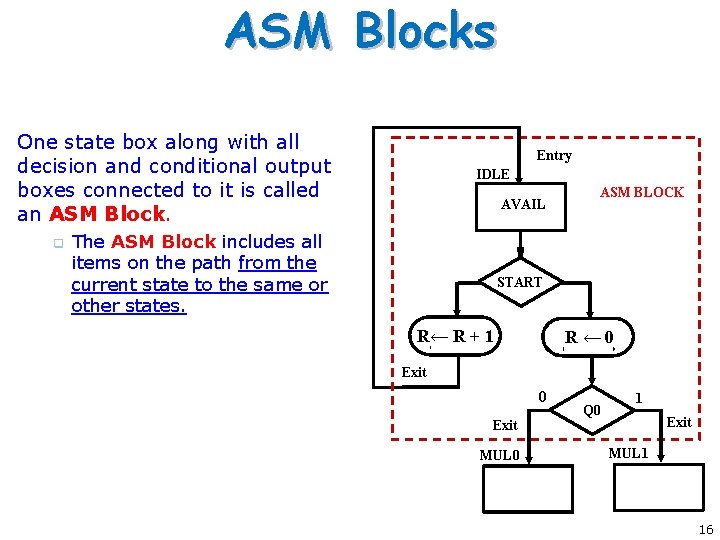
ASM Blocks One state box along with all decision and conditional output boxes connected to it is called an ASM Block. q Entry IDLE AVAIL The ASM Block includes all items on the path from the current state to the same or other states. ASM BLOCK START R← R + 1 R← 0 Exit MUL 0 Q 0 1 Exit MUL 1 16
State Diagram ASM
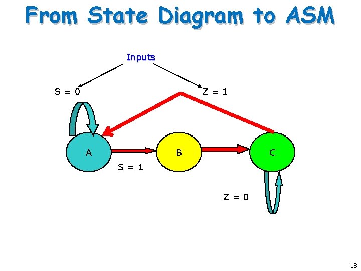
From State Diagram to ASM Inputs S=0 Z=1 A B C S=1 Z=0 18
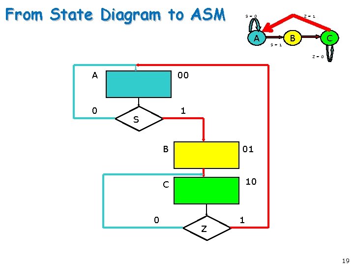
From State Diagram to ASM S=0 A Z=1 S=1 B C Z=0 A 00 0 1 S B 01 10 C 0 Z 1 19
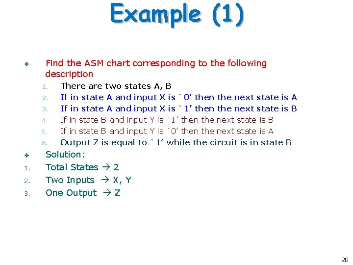
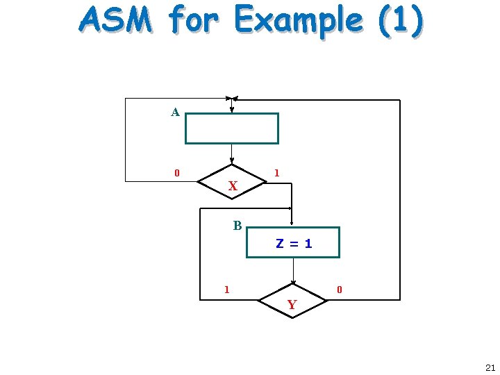
Example (1) v Find the ASM chart corresponding to the following description 1. 2. 3. 4. 5. 6. v 1. 2. 3. There are two states A, B If in state A and input X is `0’ then the next state is A If in state A and input X is `1’ then the next state is B If in state B and input Y is `0’ then the next state is A Output Z is equal to `1’ while the circuit is in state B Solution: Total States 2 Two Inputs X, Y One Output Z 20
ASM for Example (1) A 0 X 1 B Z=1 1 0 Y 21
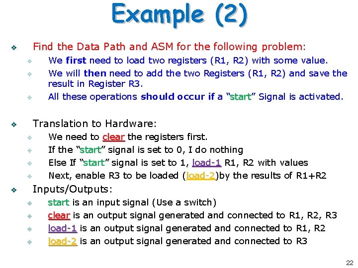
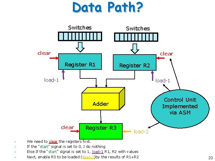
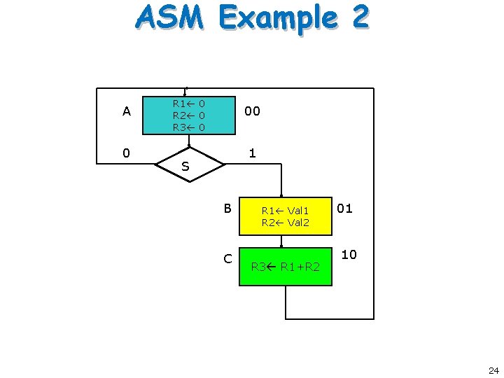
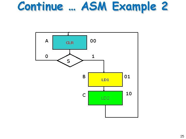
Example (2) Find the Data Path and ASM for the following problem: v We first need to load two registers (R 1, R 2) with some value. We will then need to add the two Registers (R 1, R 2) and save the result in Register R 3. All these operations should occur if a “start” start Signal is activated. v v v Translation to Hardware: v We need to clear the registers first. If the “start” start signal is set to 0, I do nothing Else If “start” start signal is set to 1, load-1 R 1, R 2 with values Next, enable R 3 to be loaded (load-2)by the results of R 1+R 2 load-2 v v v Inputs/Outputs: v v start is an input signal (Use a switch) clear is an output signal generated and connected to R 1, R 2, R 3 load-1 is an output signal generated and connected to R 1, R 2 load-2 is an output signal generated and connected to R 3 22
Data Path? Switches clear Register R 1 Register R 2 load-1 Control Unit Implemented via ASM Adder clear v v Register R 3 load-2 We need to clear the registers first. If the “start” start signal is set to 0, I do nothing Else If the “start” start signal is set to 1, load-1 R 1, R 2 with values Next, enable R 3 to be loaded ( load-2)by the results of R 1+R 2 load-2 23
ASM Example 2 A 0 R 1 0 R 2 0 R 3 0 00 1 S B C R 1 Val 1 R 2 Val 2 R 3 R 1+R 2 01 10 24
Continue … ASM Example 2 A 0 00 CLR 1 S B C LD 1 LD 2 01 10 25
Hardwired Control
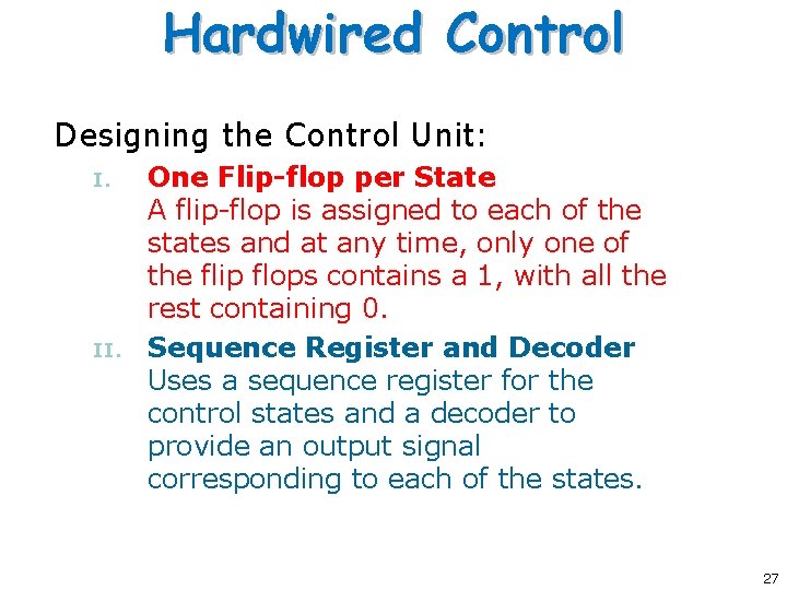
Hardwired Control Designing the Control Unit: I. II. One Flip-flop per State A flip-flop is assigned to each of the states and at any time, only one of the flip flops contains a 1, with all the rest containing 0. Sequence Register and Decoder Uses a sequence register for the control states and a decoder to provide an output signal corresponding to each of the states. 27
One Flip Flop per State
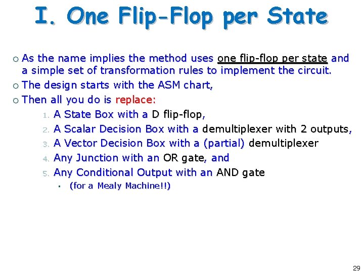
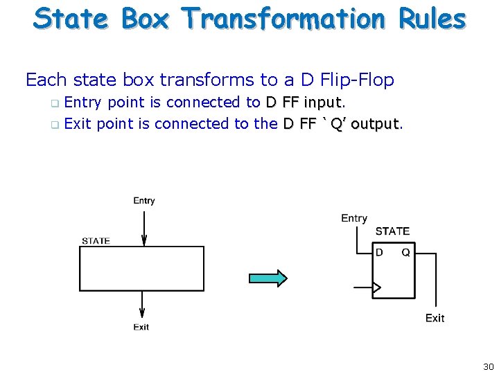
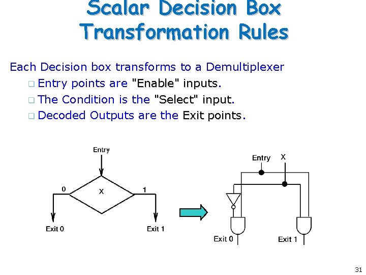
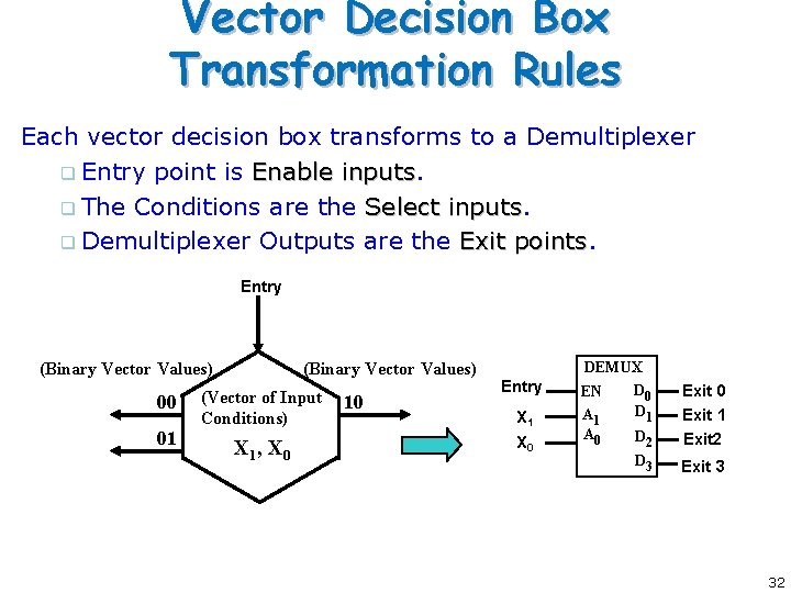
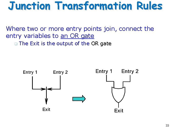
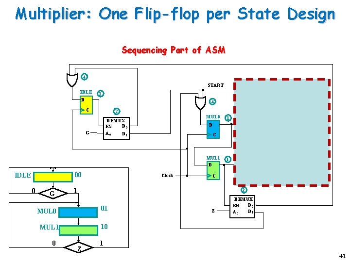
I. One Flip-Flop per State As the name implies the method uses one flip-flop per state and a simple set of transformation rules to implement the circuit. ¡ The design starts with the ASM chart, ¡ Then all you do is replace: 1. A State Box with a D flip-flop, 2. A Scalar Decision Box with a demultiplexer with 2 outputs, 3. A Vector Decision Box with a (partial) demultiplexer 4. Any Junction with an OR gate, and 5. Any Conditional Output with an AND gate ¡ • (for a Mealy Machine!!) 29
State Box Transformation Rules Each state box transforms to a D Flip-Flop Entry point is connected to D FF input q Exit point is connected to the D FF `Q’ output q 30
Scalar Decision Box Transformation Rules Each Decision box transforms to a Demultiplexer q Entry points are "Enable" inputs q The Condition is the "Select" input q Decoded Outputs are the Exit points 31
Vector Decision Box Transformation Rules Each vector decision box transforms to a Demultiplexer q Entry point is Enable inputs q The Conditions are the Select inputs q Demultiplexer Outputs are the Exit points Entry (Binary Vector Values) 00 01 (Binary Vector Values) (Vector of Input Conditions) X 1 , X 0 10 Entry X 1 X 0 DEMUX D 0 EN D 1 A 0 D 2 Exit 0 Exit 1 Exit 2 D 3 Exit 3 32
Junction Transformation Rules Where two or more entry points join, connect the entry variables to an OR gate q The Exit is the output of the OR gate 33
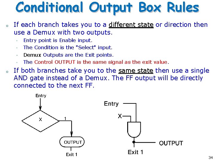
Conditional Output Box Rules o If each branch takes you to a different state or direction then use a Demux with two outputs. • • o Entry point is Enable input. The Condition is the "Select" input. Demux Outputs are the Exit points. The Control OUTPUT is the same signal as the exit value. If both branches take you to the same state then use a single AND gate instead of a Demux. The FF output will be directly connected to the next FF. 34
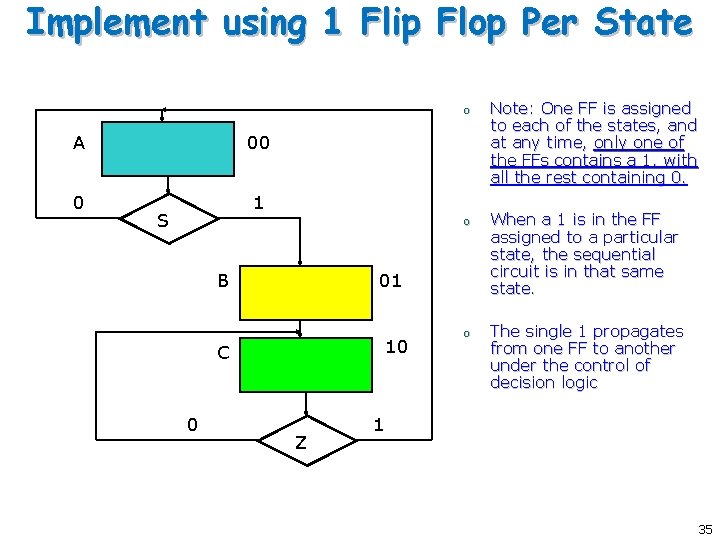
Implement using 1 Flip Flop Per State o A 00 0 1 S o B 01 10 C 0 Z o Note: One FF is assigned to each of the states, and at any time, only one of the FFs contains a 1, with all the rest containing 0. When a 1 is in the FF assigned to a particular state, the sequential circuit is in that same state. The single 1 propagates from one FF to another under the control of decision logic 1 35
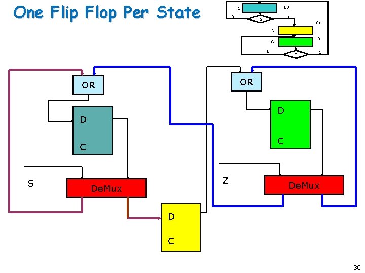
One Flip Flop Per State 00 A 0 1 S 01 B 10 C 0 1 OR OR D D C C S Z Z De. Mux D C 36
Conditional Outputs
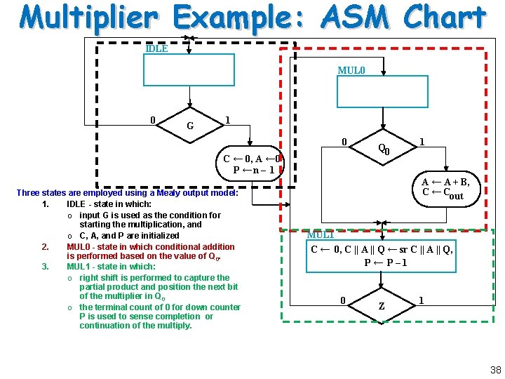
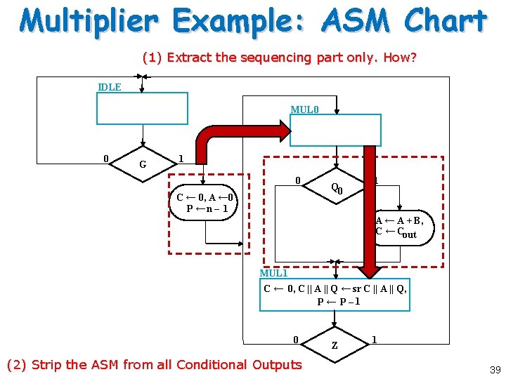
Multiplier Example: ASM Chart IDLE MUL 0 0 G 1 0 C ← 0, A ← 0 P ←n – 1 Three states are employed using a Mealy output model: 1. IDLE - state in which: o input G is used as the condition for starting the multiplication, and o C, A, and P are initialized 2. MUL 0 - state in which conditional addition is performed based on the value of Q 0. 3. MUL 1 - state in which: o right shift is performed to capture the partial product and position the next bit of the multiplier in Q 0 o the terminal count of 0 for down counter P is used to sense completion or continuation of the multiply. Q 0 1 A ← A + B, C ← Cout MUL 1 C ← 0, C || A || Q ← sr C || A || Q, P← P– 1 0 Z 1 38
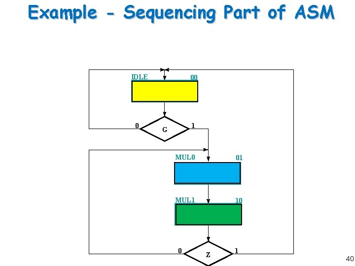
Multiplier Example: ASM Chart (1) Extract the sequencing part only. How? IDLE MUL 0 0 G 1 0 C ← 0, A ← 0 P ←n – 1 Q 0 1 A ← A + B, C ← Cout MUL 1 C ← 0, C || A || Q ← sr C || A || Q, P← P– 1 0 (2) Strip the ASM from all Conditional Outputs Z 1 39
Example - Sequencing Part of ASM IDLE 0 00 1 G MUL 0 01 MUL 1 10 0 Z 1 40
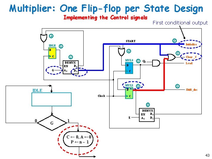
Multiplier: One Flip-flop per State Design Sequencing Part of ASM 4 5 START IDLE D 4 C 2 MUL 0 DEMUX D 0 EN A 0 D 1 G 00 0 G Clear _C 1 Q 0 Load C Clock 1 5 Shift_dec C 1 2 01 MUL 0 Z DEMUX D 0 EN D 1 A 0 10 MUL 1 0 5 D MUL 1 D IDLE Initialize 1 Z 1 41
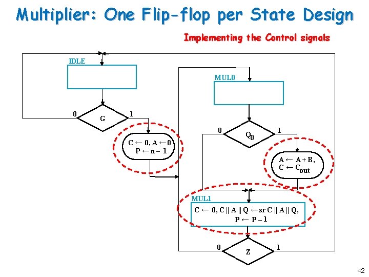
Multiplier: One Flip-flop per State Design Implementing the Control signals IDLE MUL 0 0 G 1 0 C ← 0, A ← 0 P←n– 1 Q 0 1 A ← A + B, C ← Cout MUL 1 C ← 0, C || A || Q ← sr C || A || Q, P← P– 1 0 Z 1 42
Multiplier: One Flip-flop per State Design Implementing the Control signals First conditional output 4 5 START IDLE Initialize 1 D 4 C G 2 MUL 0 DEMUX D 0 EN A 0 D 1 5 Clear _C 1 Q 0 Load D C MUL 1 D IDLE Clock 1 5 Shift_dec C 2 0 G 1 Z DEMUX D 0 EN D 1 A 0 C ← 0, A ← 0 P←n– 1 43
Sequence Register & Decoder
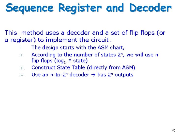
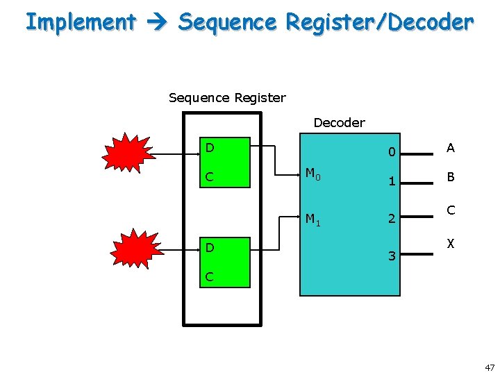
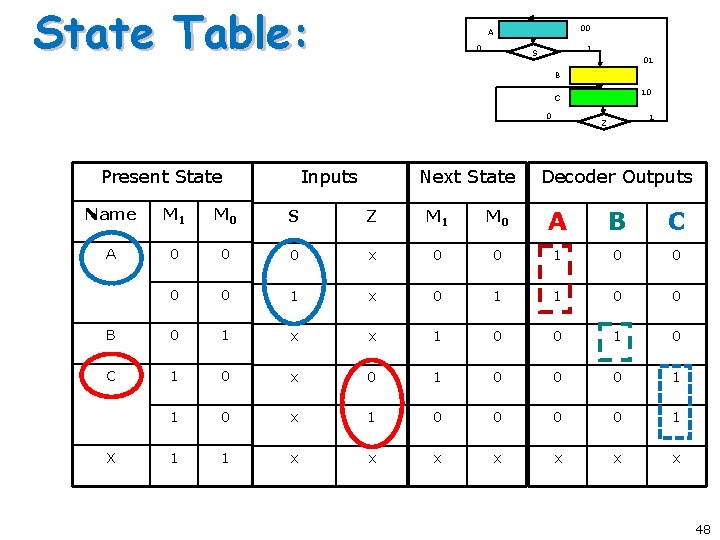
Sequence Register and Decoder This method uses a decoder and a set of flip flops (or a register) to implement the circuit. I. III. IV. The design starts with the ASM chart, According to the number of states 2 n, we will use n flip flops (log 2 # state) Construct State Table (directly from ASM) Use an n-to-2 n decoder has 2 n outputs 45
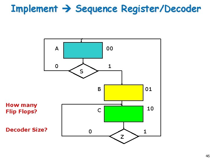
Implement Sequence Register/Decoder A 00 0 1 S B How many Flip Flops? Decoder Size? 01 10 C 0 Z 1 46
Implement Sequence Register/Decoder Sequence Register Decoder D C D 0 A M 0 1 B M 1 2 3 C X C 47
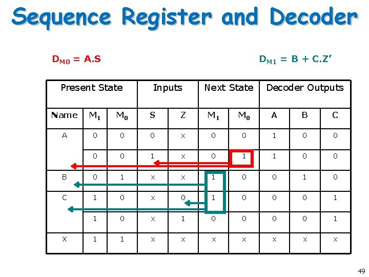
State Table: 00 A 0 1 S 01 B 10 C 0 Present State Inputs Next State 1 Z Decoder Outputs Name M 1 M 0 S Z M 1 M 0 A B C A 0 0 0 x 0 0 1 x 0 1 1 0 0 B 0 1 x x 1 0 0 1 0 C 1 0 x 0 1 0 0 0 1 1 0 x 1 0 0 1 1 1 x x x x X 48
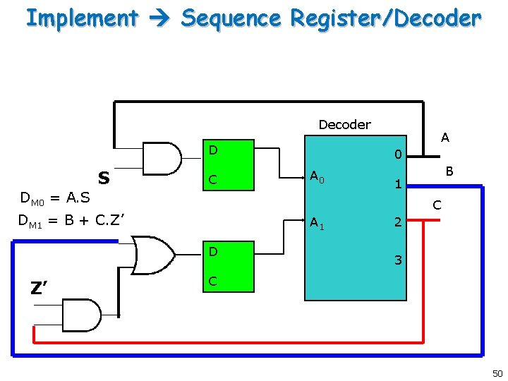
Sequence Register and Decoder DM 0 = A. S DM 1 = B + C. Z’ Present State Inputs Next State Decoder Outputs Name M 1 M 0 S Z M 1 M 0 A B C A 0 0 0 x 0 0 1 x 0 1 1 0 0 B 0 1 x x 1 0 0 1 0 C 1 0 x 0 1 0 0 0 1 1 0 x 1 0 0 1 1 1 x x x x X 49
Implement Sequence Register/Decoder D S C 0 A 0 DM 0 = A. S B 1 C DM 1 = B + C. Z’ A 1 D Z’ A 2 3 C 50
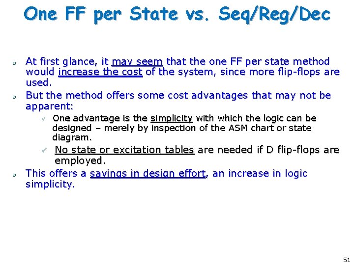
One FF per State vs. Seq/Reg/Dec o o At first glance, it may seem that the one FF per state method would increase the cost of the system, since more flip-flops are used. But the method offers some cost advantages that may not be apparent: ü One advantage is the simplicity with which the logic can be designed – merely by inspection of the ASM chart or state diagram. No state or excitation tables are needed if D flip-flops are employed. This offers a savings in design effort, an increase in logic simplicity. ü o 51
VHDL Implementation
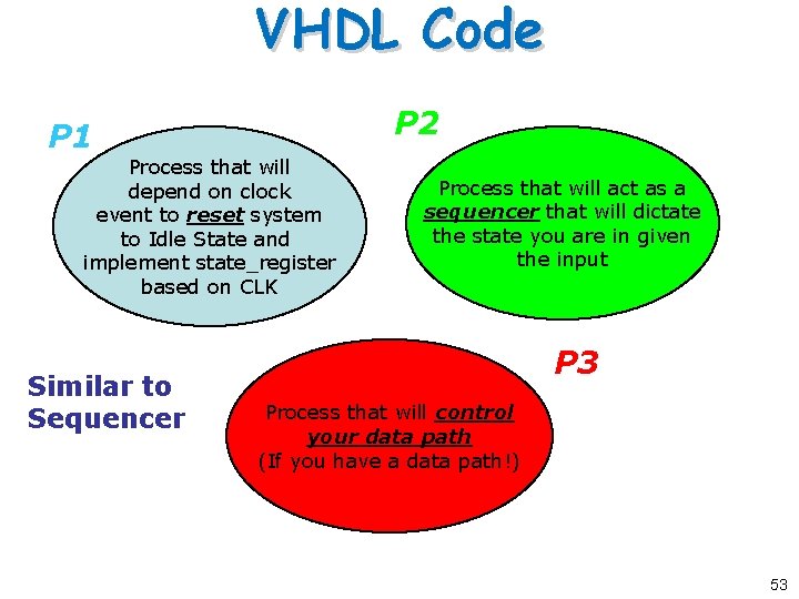
VHDL Code P 1 P 2 Process that will depend on clock event to reset system to Idle State and implement state_register based on CLK Similar to Sequencer Process that will act as a sequencer that will dictate the state you are in given the input P 3 Process that will control your data path (If you have a data path!) 53
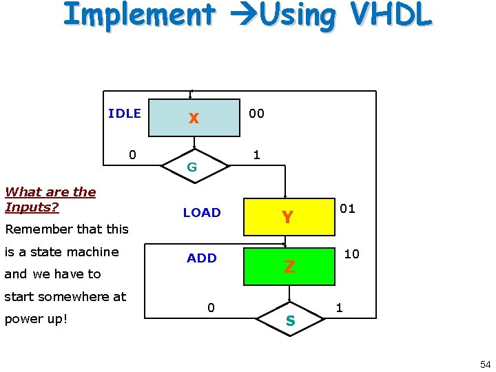
Implement Using VHDL IDLE 0 What are the Inputs? 00 X 1 G LOAD Remember that this is a state machine ADD and we have to start somewhere at power up! 0 Y 01 10 Z S 1 54
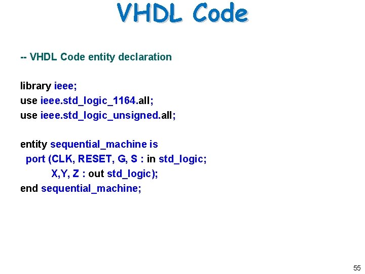
VHDL Code -- VHDL Code entity declaration library ieee; use ieee. std_logic_1164. all; use ieee. std_logic_unsigned. all; entity sequential_machine is port (CLK, RESET, G, S : in std_logic; X, Y, Z : out std_logic); end sequential_machine; 55
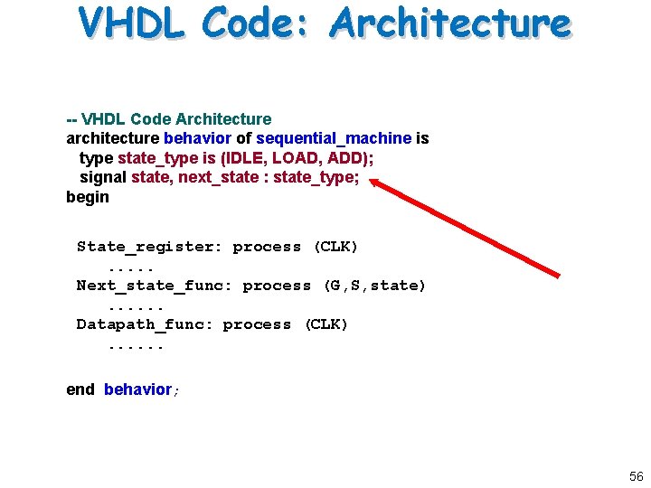
VHDL Code: Architecture -- VHDL Code Architecture architecture behavior of sequential_machine is type state_type is (IDLE, LOAD, ADD); signal state, next_state : state_type; begin State_register: process (CLK). . . Next_state_func: process (G, S, state). . . Datapath_func: process (CLK). . . end behavior; 56
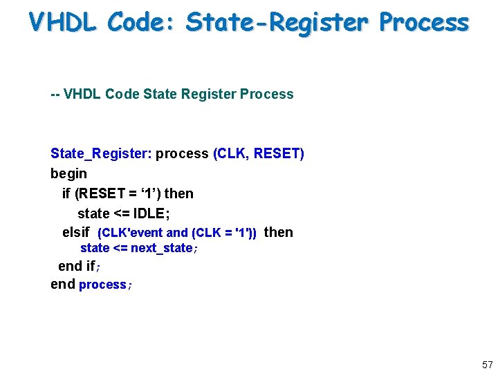
VHDL Code: State-Register Process -- VHDL Code State Register Process State_Register: process (CLK, RESET) begin if (RESET = ‘ 1’) then state <= IDLE; elsif (CLK'event and (CLK = '1')) then state <= next_state; end if; end process; 57
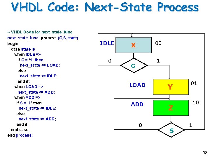
VHDL Code: Next-State Process -- VHDL Code for next_state_func: process (G, S, state) begin case state is when IDLE => if G = ‘ 1’ then next_state <= LOAD; else next_state <= IDLE; end if; when LOAD => next_state <= ADD; when ADD => if S = ‘ 1’ then next_state <= IDLE; else next_state <= ADD; end if; end case end process; IDLE 0 00 X 1 G LOAD ADD 0 Y Z S 01 10 1 58
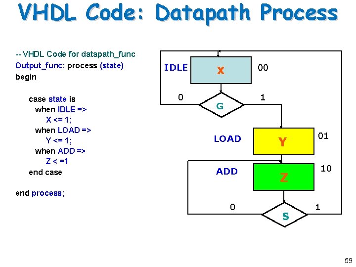
VHDL Code: Datapath Process -- VHDL Code for datapath_func Output_func: process (state) begin case state is when IDLE => X <= 1; when LOAD => Y <= 1; when ADD => Z < =1 end case IDLE 0 00 X 1 G LOAD ADD Y Z 01 10 end process; 0 S 1 59
Summary o o o Control units are an essential part of any CPU. Control units can either be programmable or non-programmable. Non-programmable CU: q q o o One FF per state Sequence Register and Decoder. Obtaining the ASM is the key to designing any control unit. Use the process statement to implement any sequential circuit, state diagrams and algorithmic state machines. 60