The Control Unit Sequencing the Processor Control Unit

- Slides: 13

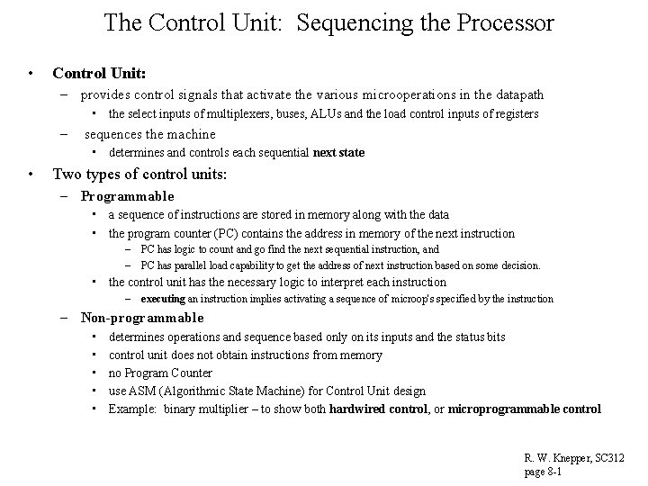
The Control Unit: Sequencing the Processor • Control Unit: – provides control signals that activate the various microoperations in the datapath • the select inputs of multiplexers, buses, ALUs and the load control inputs of registers – sequences the machine • determines and controls each sequential next state • Two types of control units: – Programmable • a sequence of instructions are stored in memory along with the data • the program counter (PC) contains the address in memory of the next instruction – PC has logic to count and go find the next sequential instruction, and – PC has parallel load capability to get the address of next instruction based on some decision. • the control unit has the necessary logic to interpret each instruction – executing an instruction implies activating a sequence of microop's specified by the instruction – Non-programmable • • • determines operations and sequence based only on its inputs and the status bits control unit does not obtain instructions from memory no Program Counter use ASM (Algorithmic State Machine) for Control Unit design Example: binary multiplier – to show both hardwired control, or microprogrammable control R. W. Knepper, SC 312 page 8 -1

ASM Chart Fundamentals • Hardware algorithm: specified as a finite number of procedural steps which perform a data processing task – Flowchart - specifies a sequence of procedural steps and decision paths for the algorithm – Finite State Machine = a sequential digital circuit – Algorithm State Machine = use of a flowchart to define digital hardware algorithms • describes a sequence of events and decision paths • describes the timing relationship between states • ASM Chart: – state box • rectangle containing register transfer op's or outputs activated while CU is in that state – decision box • diamond-shaped box with Boolean expression involving a decision with two paths – conditional output box • oval-shaped box receiving input from a decision box specifying action if condition is met R. W. Knepper, SC 312 page 8 -2

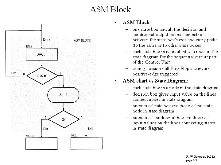
ASM Block • ASM Block: – one state box and all the decision and conditional output boxes connected between the state box's exit and entry paths (to the same or to other state boxes) – each state box is equivalent to a node in the state diagram for the sequential circuit part of the Control Unit – timing: assume all Flip-Flop's used are positive-edge triggered • ASM chart vs State Diagram: – each state box is a node in the state diagram – decision box gives input value on the lines connect nodes in state diagram – outputs of state box are those of the state node in state diagram – outputs of conditional box are those of input values on the lines connecting states in state diagram R. W. Knepper, SC 312 page 8 -3

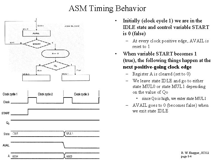
ASM Timing Behavior • Initially (clock cycle 1) we are in the IDLE state and control variable START is 0 (false) – At every clock positive edge, AVAIL is reset to 1 • When variable START becomes 1 (true), the following things happen at the next positive-going clock edge – Register A is cleared (set to 0) – We leave state IDLE and go to either state MUL 0 or state MUL 1 depending on the value of Qo • since Qo is high, we enter state MUL 1 – AVAIL goes to 0 (becomes false) when we exit state IDLE R. W. Knepper, SC 312 page 8 -4

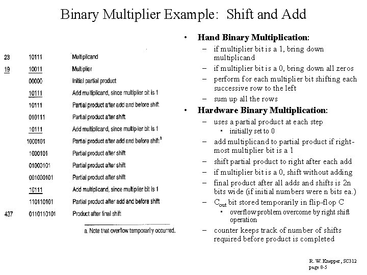
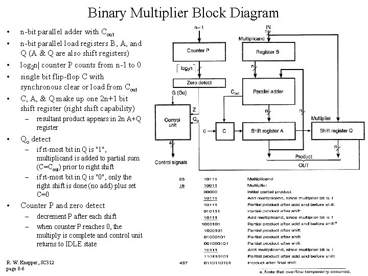
Binary Multiplier Example: Shift and Add • Hand Binary Multiplication: – if multiplier bit is a 1, bring down multiplicand – if multiplier bit is a 0, bring down all zeros – perform for each multiplier bit shifting each successive row to the left – sum up all the rows • Hardware Binary Multiplication: – uses a partial product at each step • initially set to 0 – add multiplicand to partial product if rightmost multiplier bit is a 1 – shift partial product to right after each add – if multiplier bit is a 0, shift without adding – final product after all adds and shifts is 2 n bits wide (if initial numbers were n bits ea. ) – Cout bit stored temporarily in flip-flop C • overflow problem overcome by right shift operation – counter keeps track of number of shifts required before product is completed R. W. Knepper, SC 312 page 8 -5

Binary Multiplier Block Diagram • • • n-bit parallel adder with Cout n-bit parallel load registers B, A, and Q (A & Q are also shift registers) log 2 n| counter P counts from n-1 to 0 single bit flip-flop C with synchronous clear or load from Cout C, A, & Q make up one 2 n+1 bit shift register (right shift capability) – • Qo detect – – • resultant product appears in 2 n A+Q register if rt-most bit in Q is "1", multiplicand is added to partial sum (C=Cout) prior to right shift if rt-most bit in Q is "0", only the right shift is done (no add) plus set C=0 Counter P and zero detect – – decrement P after each shift when counter P reaches 0, the multiply is complete and control unit returns to IDLE state R. W. Knepper, SC 312 page 8 -6

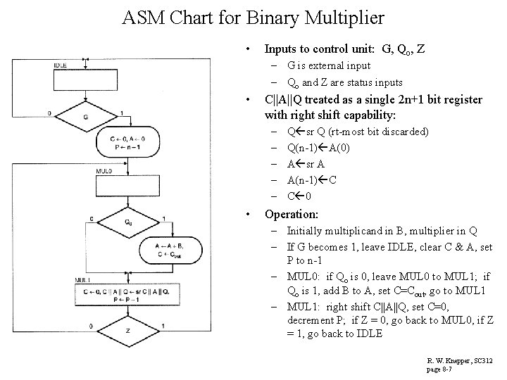
ASM Chart for Binary Multiplier • Inputs to control unit: G, Qo, Z – G is external input – Qo and Z are status inputs • C||A||Q treated as a single 2 n+1 bit register with right shift capability: – – – • Q sr Q (rt-most bit discarded) Q(n-1) A(0) A sr A A(n-1) C C 0 Operation: – Initially multiplicand in B, multiplier in Q – If G becomes 1, leave IDLE, clear C & A, set P to n-1 – MUL 0: if Qo is 0, leave MUL 0 to MUL 1; if Qo is 1, add B to A, set C=Cout, go to MUL 1 – MUL 1: right shift C||A||Q, set C=0, decrement P; if Z = 0, go back to MUL 0, if Z = 1, go back to IDLE R. W. Knepper, SC 312 page 8 -7

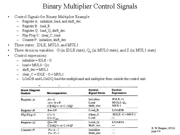
Binary Multiplier Control Signals • Control Signals for Binary Multiplier Example – – – • • • Register A: initialize, load, and shift_dec Register B: load_B Register Q: load_Q, shift_dec Flip-Flop C: clear_C, load Counter P: initialize, shift_dec Three states: IDLE, MUL 0, and MUL 1 Three decision variables: G (in IDLE state), Qo (in MUL 0 state), and Z (in MUL 1 state) Control expressions: – – – initialize = IDLE · G load = MUL 0 · Qo shift_dec = MUL 1 clear_C = IDLE · G + MUL 1 LOADB and LOADQ load the multiplicand multiplier from outside the control unit R. W. Knepper, SC 312 page 8 -8

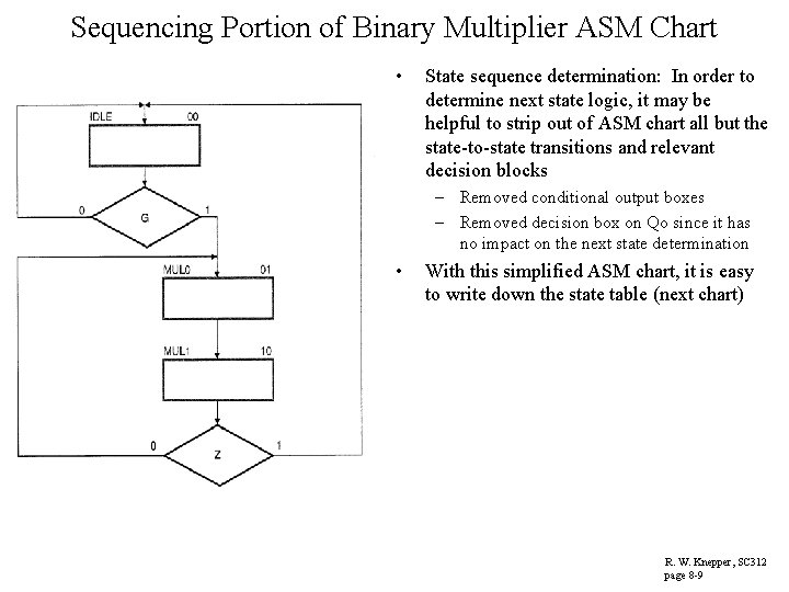
Sequencing Portion of Binary Multiplier ASM Chart • State sequence determination: In order to determine next state logic, it may be helpful to strip out of ASM chart all but the state-to-state transitions and relevant decision blocks – Removed conditional output boxes – Removed decision box on Qo since it has no impact on the next state determination • With this simplified ASM chart, it is easy to write down the state table (next chart) R. W. Knepper, SC 312 page 8 -9

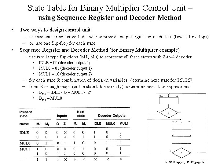
State Table for Binary Multiplier Control Unit – using Sequence Register and Decoder Method • Two ways to design control unit: – use sequence register with decoder to provide output signal for each state (fewest flip-flops) – or, use one flip-flop for each state • Sequence Register and Decoder Method (for Binary Multiplier example): – use two D type flip-flops (M 1, M 0) to represent all three states with 2 -to-4 decoder • IDLE = 00 (decoder output 0) • MUL 0 = 01 (decoder output 1) • MUL 1 = 10 (decoder output 2) – for each state & combination of decision variables, determine next state for M 1, M 0 – from Karnaugh maps (or the state table directly), determine next state expressions • DMo = IDLE · G + MUL 1 · Z' • DM 1 = MUL 0 R. W. Knepper, SC 312, page 8 -10

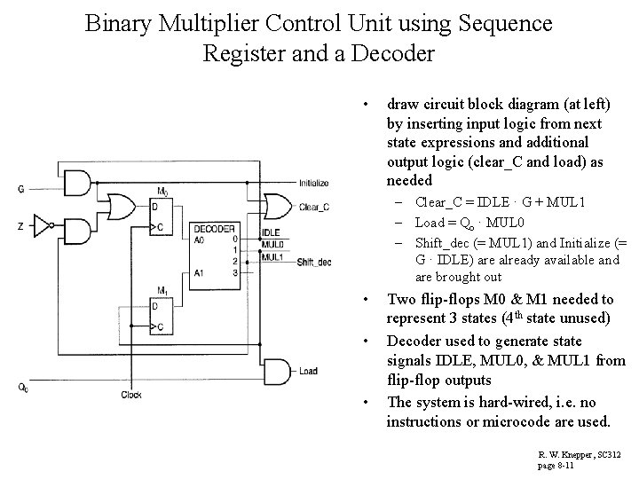
Binary Multiplier Control Unit using Sequence Register and a Decoder • draw circuit block diagram (at left) by inserting input logic from next state expressions and additional output logic (clear_C and load) as needed – Clear_C = IDLE · G + MUL 1 – Load = Qo · MUL 0 – Shift_dec (= MUL 1) and Initialize (= G · IDLE) are already available and are brought out • • • Two flip-flops M 0 & M 1 needed to represent 3 states (4 th state unused) Decoder used to generate state signals IDLE, MUL 0, & MUL 1 from flip-flop outputs The system is hard-wired, i. e. no instructions or microcode are used. R. W. Knepper, SC 312 page 8 -11

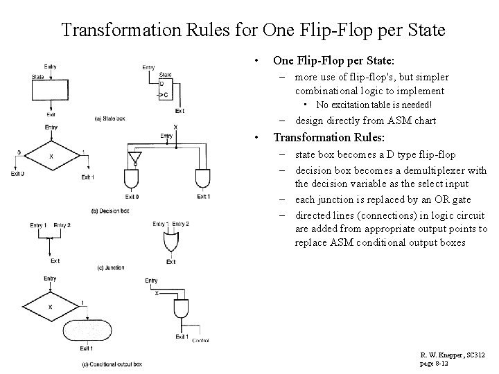
Transformation Rules for One Flip-Flop per State • One Flip-Flop per State: – more use of flip-flop's, but simpler combinational logic to implement • No excitation table is needed! – design directly from ASM chart • Transformation Rules: – state box becomes a D type flip-flop – decision box becomes a demultiplexer with the decision variable as the select input – each junction is replaced by an OR gate – directed lines (connections) in logic circuit are added from appropriate output points to replace ASM conditional output boxes R. W. Knepper, SC 312 page 8 -12

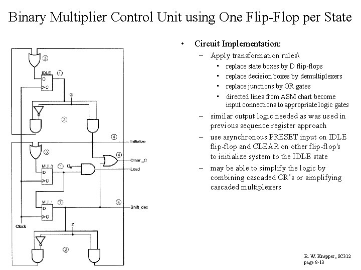
Binary Multiplier Control Unit using One Flip-Flop per State • Circuit Implementation: – Apply transformation rules • • replace state boxes by D flip-flops replace decision boxes by demultiplexers replace junctions by OR gates directed lines from ASM chart become input connections to appropriate logic gates – similar output logic needed as was used in previous sequence register approach – use asynchronous PRESET input on IDLE flip-flop and CLEAR on other flip-flop's to initialize system to the IDLE state – may be able to simplify the logic by combining cascaded OR’s or simplifying cascaded multiplexers R. W. Knepper, SC 312 page 8 -13