Digital Electronics 7 Semiconductor Memory Semiconductor Memory Introduction
![RAM (cont. ) • Read operation example: Read one byte at location A[1: 0] RAM (cont. ) • Read operation example: Read one byte at location A[1: 0]](https://slidetodoc.com/presentation_image_h/b62f3751ad2a01055279a60185397600/image-16.jpg)
![RAM (cont. ) • Write operation example: Write one byte at location A[1: 0] RAM (cont. ) • Write operation example: Write one byte at location A[1: 0]](https://slidetodoc.com/presentation_image_h/b62f3751ad2a01055279a60185397600/image-17.jpg)

- Slides: 22

Digital Electronics 7 –Semiconductor Memory

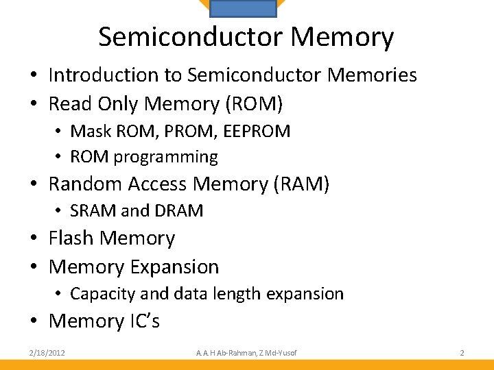
Semiconductor Memory • Introduction to Semiconductor Memories • Read Only Memory (ROM) • Mask ROM, PROM, EEPROM • ROM programming • Random Access Memory (RAM) • SRAM and DRAM • Flash Memory • Memory Expansion • Capacity and data length expansion • Memory IC’s 2/18/2012 A. A. H Ab-Rahman, Z. Md-Yusof 2

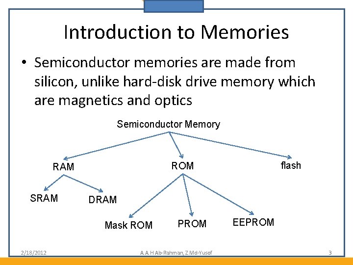
Introduction to Memories • Semiconductor memories are made from silicon, unlike hard-disk drive memory which are magnetics and optics Semiconductor Memory SRAM DRAM Mask ROM 2/18/2012 flash ROM RAM PROM A. A. H Ab-Rahman, Z. Md-Yusof EEPROM 3

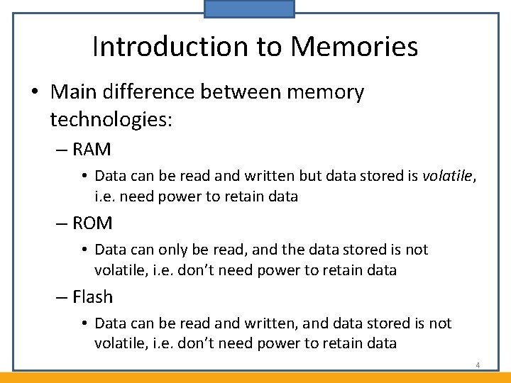
Introduction to Memories • Main difference between memory technologies: – RAM • Data can be read and written but data stored is volatile, i. e. need power to retain data – ROM • Data can only be read, and the data stored is not volatile, i. e. don’t need power to retain data – Flash • Data can be read and written, and data stored is not volatile, i. e. don’t need power to retain data 4

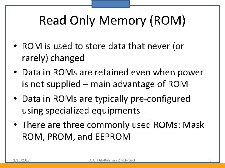
Read Only Memory (ROM) • ROM is used to store data that never (or rarely) changed • Data in ROMs are retained even when power is not supplied – main advantage of ROM • Data in ROMs are typically pre-configured using specialized equipments • There are three commonly used ROMs: Mask ROM, PROM, and EEPROM 2/18/2012 A. A. H Ab-Rahman, Z. Md-Yusof 5

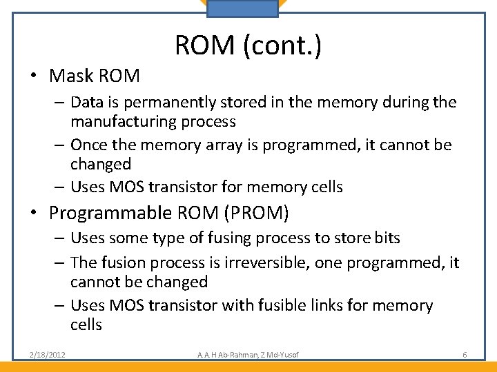
• Mask ROM (cont. ) – Data is permanently stored in the memory during the manufacturing process – Once the memory array is programmed, it cannot be changed – Uses MOS transistor for memory cells • Programmable ROM (PROM) – Uses some type of fusing process to store bits – The fusion process is irreversible, one programmed, it cannot be changed – Uses MOS transistor with fusible links for memory cells 2/18/2012 A. A. H Ab-Rahman, Z. Md-Yusof 6

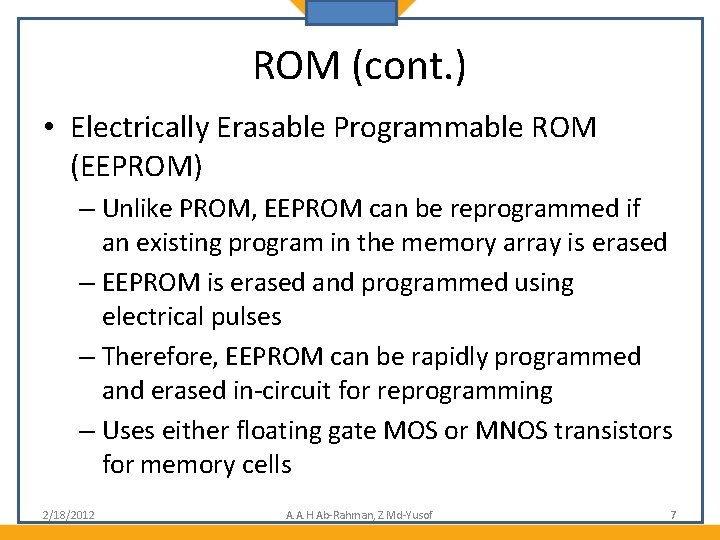
ROM (cont. ) • Electrically Erasable Programmable ROM (EEPROM) – Unlike PROM, EEPROM can be reprogrammed if an existing program in the memory array is erased – EEPROM is erased and programmed using electrical pulses – Therefore, EEPROM can be rapidly programmed and erased in-circuit for reprogramming – Uses either floating gate MOS or MNOS transistors for memory cells 2/18/2012 A. A. H Ab-Rahman, Z. Md-Yusof 7

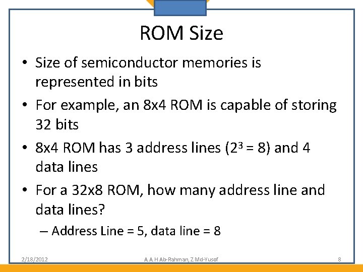
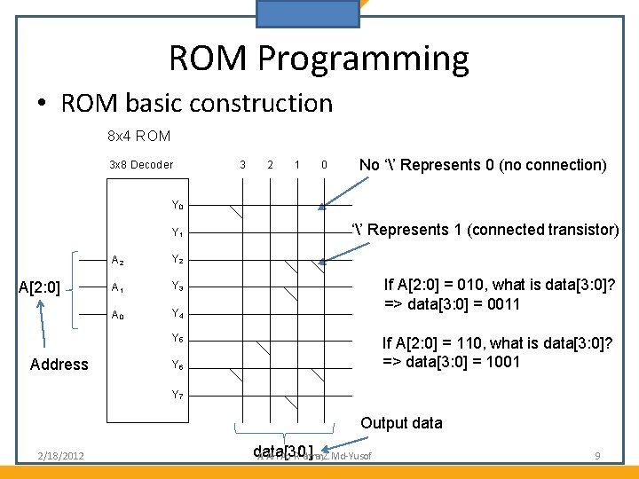
ROM Size • Size of semiconductor memories is represented in bits • For example, an 8 x 4 ROM is capable of storing 32 bits • 8 x 4 ROM has 3 address lines (23 = 8) and 4 data lines • For a 32 x 8 ROM, how many address line and data lines? – Address Line = 5, data line = 8 2/18/2012 A. A. H Ab-Rahman, Z. Md-Yusof 8

ROM Programming • ROM basic construction 8 x 4 ROM 3 x 8 Decoder 3 2 1 0 No ‘’ Represents 0 (no connection) Y 0 Y 1 A[2: 0] A 2 Y 2 A 1 Y 3 A 0 Y 4 ‘’ Represents 1 (connected transistor) If A[2: 0] = 010, what is data[3: 0]? => data[3: 0] = 0011 Y 5 Address If A[2: 0] = 110, what is data[3: 0]? => data[3: 0] = 1001 Y 6 Y 7 Output data 2/18/2012 d. A. a. A. t. Ha. A[b 3 -R: 0 ah]man, Z. Md-Yusof 9

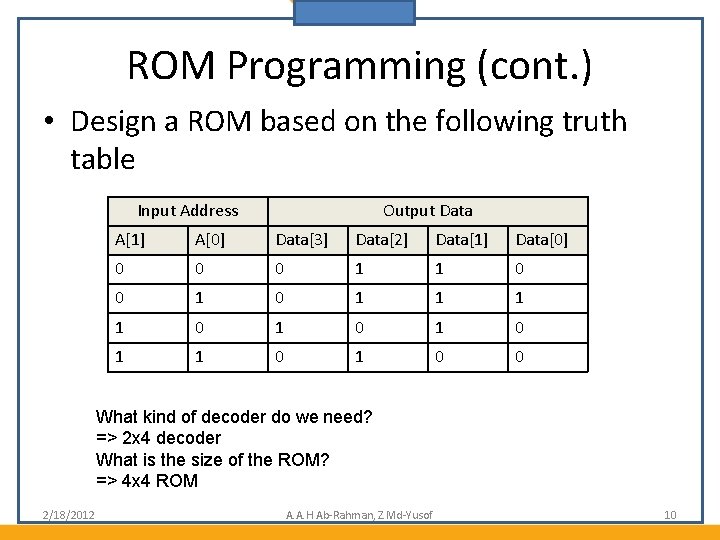
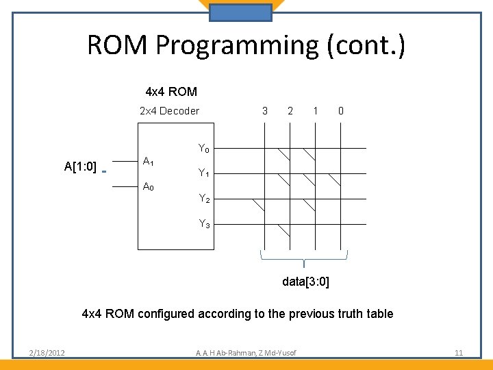
ROM Programming (cont. ) • Design a ROM based on the following truth table Input Address Output Data A[1] A[0] Data[3] Data[2] Data[1] Data[0] 0 0 0 1 1 1 1 0 1 0 1 0 0 What kind of decoder do we need? => 2 x 4 decoder What is the size of the ROM? => 4 x 4 ROM 2/18/2012 A. A. H Ab-Rahman, Z. Md-Yusof 10

ROM Programming (cont. ) 4 x 4 ROM 2 x 4 Decoder 3 2 1 0 Y 0 A[1: 0] A 1 A 0 Y 1 Y 2 Y 3 data[3: 0] 4 x 4 ROM configured according to the previous truth table 2/18/2012 A. A. H Ab-Rahman, Z. Md-Yusof 11

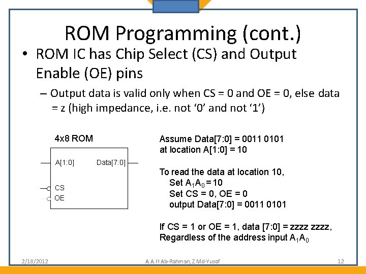
ROM Programming (cont. ) • ROM IC has Chip Select (CS) and Output Enable (OE) pins – Output data is valid only when CS = 0 and OE = 0, else data = z (high impedance, i. e. not ‘ 0’ and not ‘ 1’) 4 x 8 ROM A[1: 0] CS OE Assume Data[7: 0] = 0011 0101 at location A[1: 0] = 10 Data[7: 0] To read the data at location 10, Set A 1 A 0 = 10 Set CS = 0, OE = 0 output Data[7: 0] = 0011 0101 If CS = 1 or OE = 1, data [7: 0] = zzzz, Regardless of the address input A 1 A 0 2/18/2012 A. A. H Ab-Rahman, Z. Md-Yusof 12

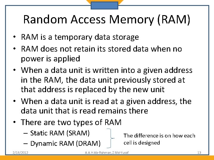
Random Access Memory (RAM) • RAM is a temporary data storage • RAM does not retain its stored data when no power is applied • When a data unit is written into a given address in the RAM, the data unit previously stored at that address is replaced by the new unit • When a data unit is read at a given address, the data unit that is read remains there • There are two types of RAM – Static RAM (SRAM) – Dynamic RAM (DRAM) 2/18/2012 The difference is on how each cell is designed A. A. H Ab-Rahman, Z. Md-Yusof 13

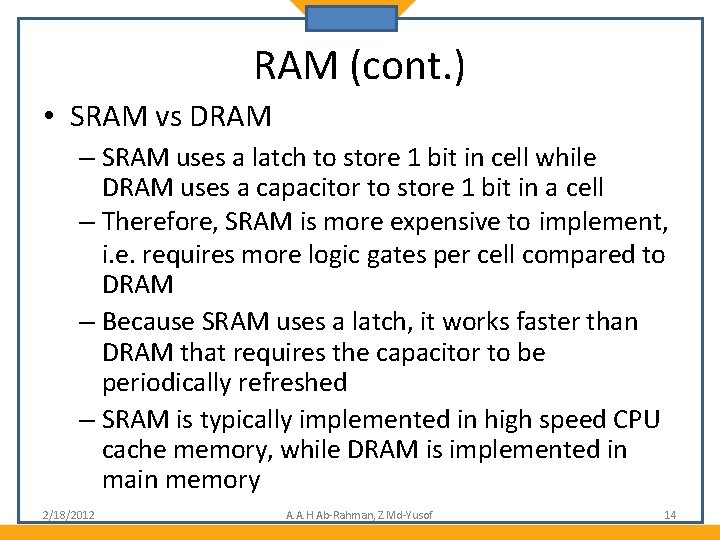
RAM (cont. ) • SRAM vs DRAM – SRAM uses a latch to store 1 bit in cell while DRAM uses a capacitor to store 1 bit in a cell – Therefore, SRAM is more expensive to implement, i. e. requires more logic gates per cell compared to DRAM – Because SRAM uses a latch, it works faster than DRAM that requires the capacitor to be periodically refreshed – SRAM is typically implemented in high speed CPU cache memory, while DRAM is implemented in main memory 2/18/2012 A. A. H Ab-Rahman, Z. Md-Yusof 14

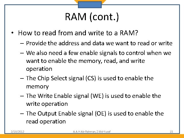
RAM (cont. ) • How to read from and write to a RAM? – Provide the address and data we want to read or write – We also need a few enable signals to control when we want to enable the memory, read, and write operation – The Chip Select signal (CS) is used to enable the memory – The Write Enable signal (WE) is used to enable the write operation – The Output Enable signal (OE) is used to enable the read operation 2/18/2012 A. A. H Ab-Rahman, Z. Md-Yusof 15
![RAM cont Read operation example Read one byte at location A1 0 RAM (cont. ) • Read operation example: Read one byte at location A[1: 0]](https://slidetodoc.com/presentation_image_h/b62f3751ad2a01055279a60185397600/image-16.jpg)
RAM (cont. ) • Read operation example: Read one byte at location A[1: 0] = 10 from a 4 x 8 RAM 10 0 0 1 A[1: 0] CS OE WE Step 1: Supply address A[1: 0] = 10 to Read location 10 Data[7: 0] Step 2: Set CS = 0 to enable the memory Step 3: Set OE = 0 to enable read Step 4: Set WE = 1 to disable write Step 5: Get the data at location 10 2/18/2012 A. A. H Ab-Rahman, Z. Md-Yusof 16
![RAM cont Write operation example Write one byte at location A1 0 RAM (cont. ) • Write operation example: Write one byte at location A[1: 0]](https://slidetodoc.com/presentation_image_h/b62f3751ad2a01055279a60185397600/image-17.jpg)
RAM (cont. ) • Write operation example: Write one byte at location A[1: 0] = 10 from a 4 x 8 RAM Step 1: Supply address A[1: 0] = 10 to write location 10 4 x 8 RAM 10 0 1 0 A[1: 0] Data[7: 0] Step 2: Supply the Data[7: 0] to write Example: 1010 0111 CS OE Step 2: Set CS = 0 to enable the memory WE Step 3: Set OE = 1 to disable read Step 4: Set WE = 0 to enable write Step 5: data[7: 0] is written at location 10 2/18/2012 A. A. H Ab-Rahman, Z. Md-Yusof 17

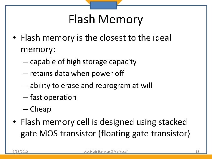
Flash Memory • Flash memory is the closest to the ideal memory: – capable of high storage capacity – retains data when power off – ability to erase and reprogram at will – fast operation – Cheap • Flash memory cell is designed using stacked gate MOS transistor (floating gate transistor) 2/18/2012 A. A. H Ab-Rahman, Z. Md-Yusof 18

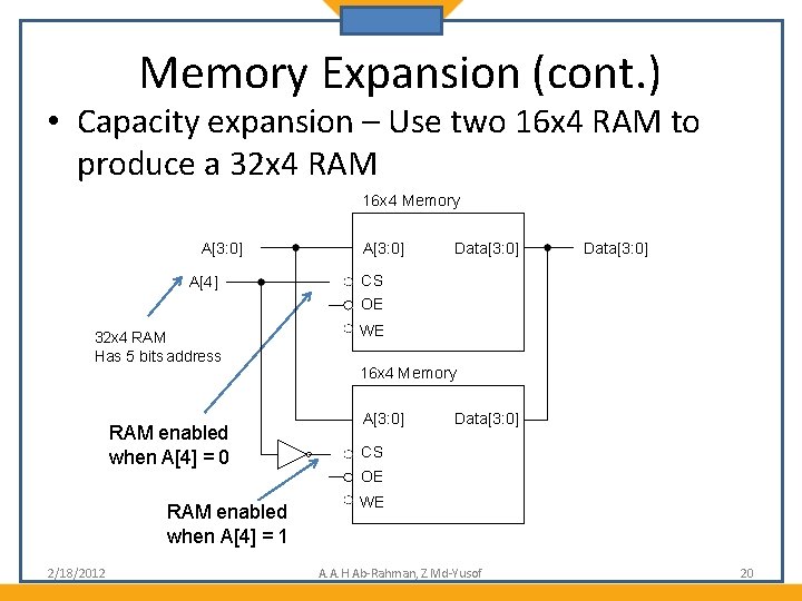
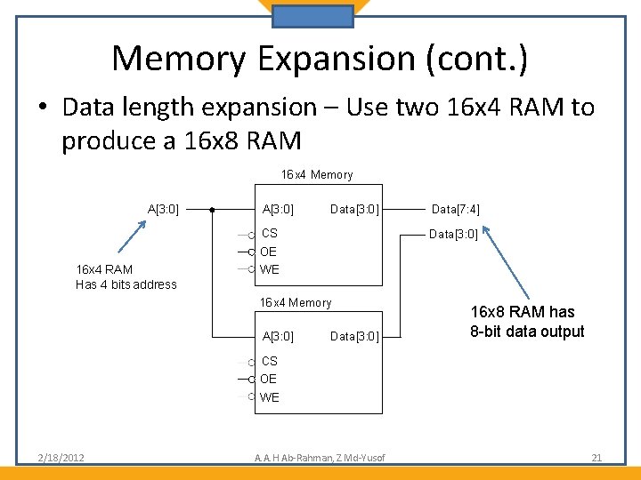
Memory Expansion • Memory can be expanded on its capacity or data length – Capacity expansion example: 16 x 4 memory expands to 32 x 4 memory – Data length expansion example: 16 x 4 memory expands to 16 x 8 memory 2/18/2012 A. A. H Ab-Rahman, Z. Md-Yusof 19

Memory Expansion (cont. ) • Capacity expansion – Use two 16 x 4 RAM to produce a 32 x 4 RAM 16 x 4 Memory A[3: 0] A[4] CS OE 32 x 4 RAM Has 5 bits address WE RAM enabled when A[4] = 0 RAM enabled when A[4] = 1 2/18/2012 Data[3: 0] 16 x 4 Memory A[3: 0] Data[3: 0] CS OE WE A. A. H Ab-Rahman, Z. Md-Yusof 20

Memory Expansion (cont. ) • Data length expansion – Use two 16 x 4 RAM to produce a 16 x 8 RAM 16 x 4 Memory A[3: 0] Data[3: 0] CS Data[7: 4] Data[3: 0] OE 16 x 4 RAM Has 4 bits address WE 16 x 4 Memory A[3: 0] Data[3: 0] 16 x 8 RAM has 8 -bit data output CS OE WE 2/18/2012 A. A. H Ab-Rahman, Z. Md-Yusof 21

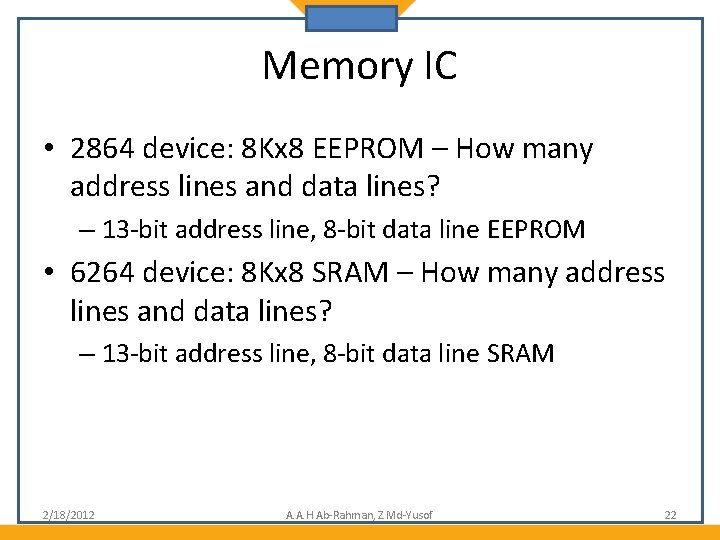
Memory IC • 2864 device: 8 Kx 8 EEPROM – How many address lines and data lines? – 13 -bit address line, 8 -bit data line EEPROM • 6264 device: 8 Kx 8 SRAM – How many address lines and data lines? – 13 -bit address line, 8 -bit data line SRAM 2/18/2012 A. A. H Ab-Rahman, Z. Md-Yusof 22