
ENG 2410 Digital Design Week 6 Sequential Circuits










- Slides: 74
ENG 2410 Digital Design: Week #6 “Sequential Circuits: Part A” S. Areibi School of Engineering University of Guelph
Topics ¡ Sequential Circuit Definitions l l ¡ ¡ Latches Flip-Flops Delays in Sequential Circuits Clock Gating
Resources Chapter #6, Mano Sections l l l 6. 1 Sequential Circuit Definition 6. 2 Latches 6. 3 Flip-Flops
Combinational Circuits vs. Sequential Circuits
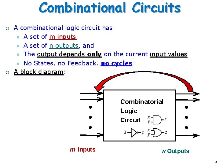
Combinational Circuits ¡ ¡ A combinational logic circuit has: l A set of m inputs, inputs l A set of n outputs, outputs and l The output depends only on the current input values l No States, no Feedback, no cycles A block diagram: diagram Combinatorial Logic Circuit m Inputs n Outputs 5
Combinational vs. Sequential Circuits o o Combinational logic are very interesting and useful for designing arithmetic circuits (adders, multipliers) or in other words the Data Path of a computer. q Combinational circuits cannot remember what happened in the past (i. e. outputs are a function of current inputs). In certain cases we might need to store some info before we proceed with our computation or take action based on a certain state that happened in the past. q Sequential circuits are capable of storing information between operations. They are useful in designing registers, counters, and Control Circuits 6
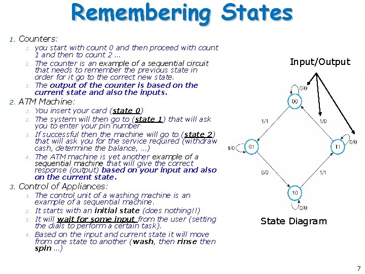
Remembering States 1. Counters: Counters 1. 2. 3. 2. Input/Output ATM Machine: Machine 1. 2. 3. 4. 3. you start with count 0 and then proceed with count 1 and then to count 2 … The counter is an example of a sequential circuit that needs to remember the previous state in order for it go to the correct new state. The output of the counter is based on the current state and also the inputs. You insert your card (state 0) The system will then go to (state 1) that will ask you to enter your pin number If successful then the machine will go to (state 2) that will ask you for the service required (withdraw cash, determine the balance, …) The ATM machine is yet another example of a sequential machine that will give the correct response (output) based on your input and also on the current state. Control of Appliances: Appliances 1. 2. 3. 4. The control unit of a washing machine is an example of a sequential machine. It starts with an initial state (does nothing!!) It will wait for some input from the user (setting the dials to perform a certain task). Based on the input and current state it will move from one state to another (wash, wash then rinse then spin …) State Diagram 7
Sequential Circuits
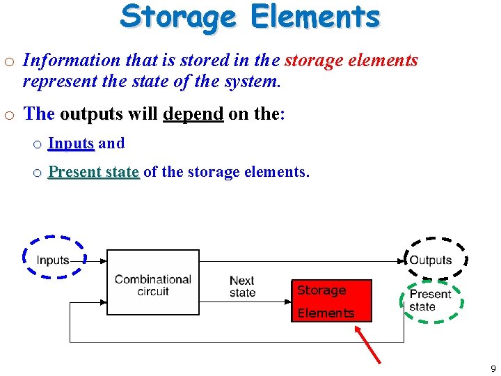
Storage Elements o Information that is stored in the storage elements represent the state of the system. o The outputs will depend on the: o Inputs and o Present state of the storage elements. Storage Elements 9
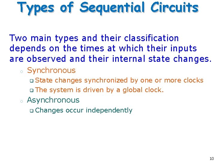
Types of Sequential Circuits Two main types and their classification depends on the times at which their inputs are observed and their internal state changes. o Synchronous State changes synchronized by one or more clocks q The system is driven by a global clock. q o Asynchronous q Changes occur independently 10
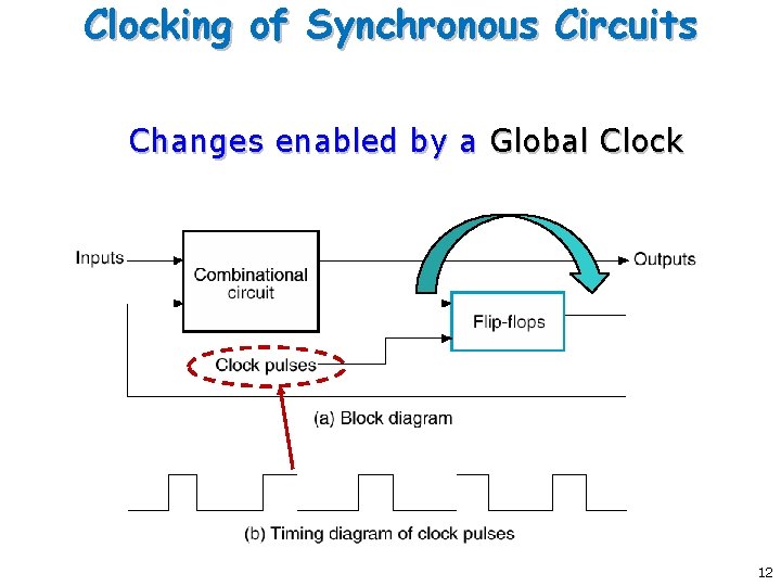
Clocking of Synchronous Circuits Changes enabled by a Global Clock 12
Latches
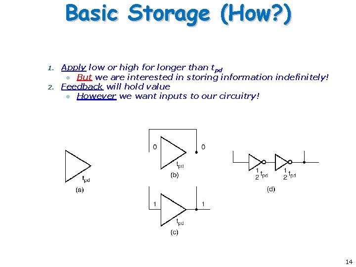
Basic Storage (How? ) 1. 2. Apply low or high for longer than tpd l But we are interested in storing information indefinitely! Feedback will hold value l However we want inputs to our circuitry! 14
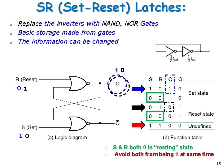
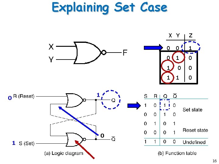
SR (Set-Reset) Latches: o o o Replace the inverters with NAND, NOR Gates Basic storage made from gates The information can be changed 10 01 10 o S & R both 0 in “resting” state o Avoid both from being 1 at same time 15
Explaining Set Case X Y Z 0 0 1 0 1 1 0 0 1 16
Latches are storage elements that can maintain a binary state indefinitely (as long as power is delivered to the circuit) until directed by an input signal to switch states. Latches are asynchronous circuits q Latches are used to build more complex synchronous circuits such as Flip Flops. q 17
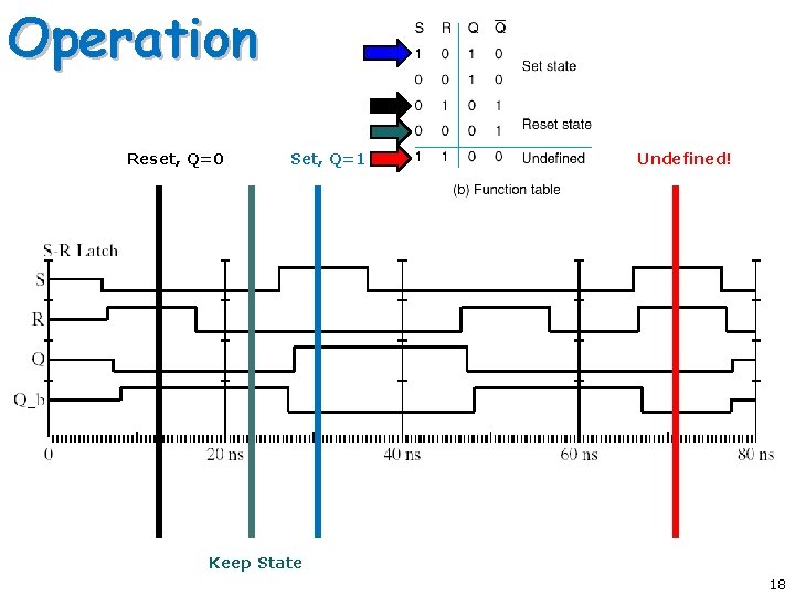
Operation Reset, Q=0 Set, Q=1 Undefined! Keep State 18
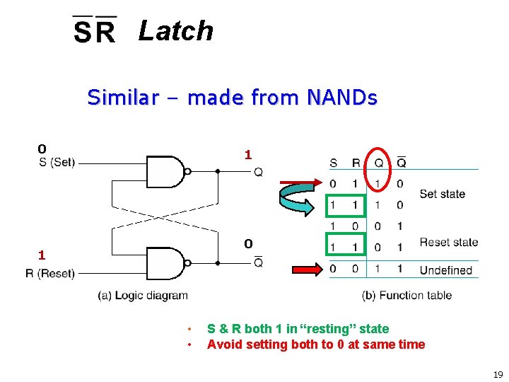
Latch Similar – made from NANDs 0 1 • • S & R both 1 in “resting” state Avoid setting both to 0 at same time 19
Latch + Control
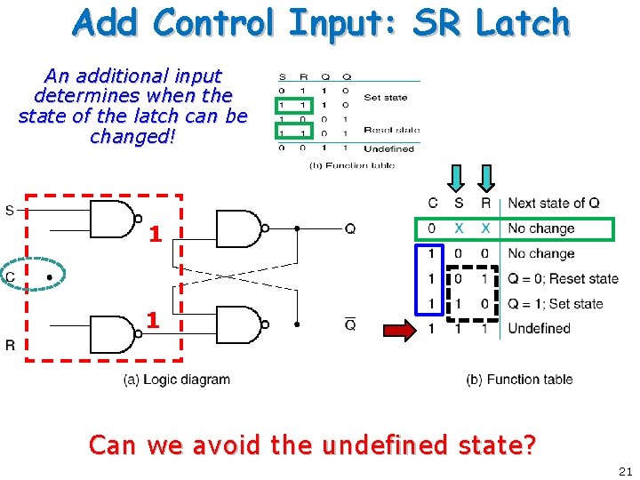
Add Control Input: SR Latch An additional input determines when the state of the latch can be changed! 1 1 Can we avoid the undefined state? 21
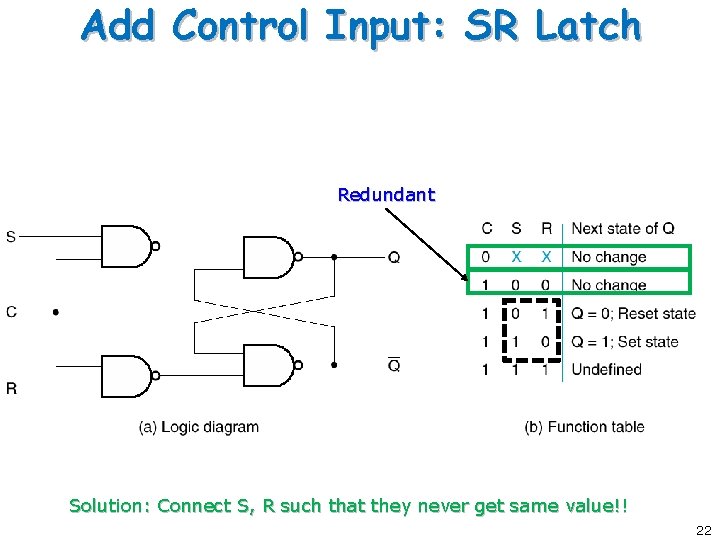
Add Control Input: SR Latch Redundant Solution: Connect S, R such that they never get same value!! 22
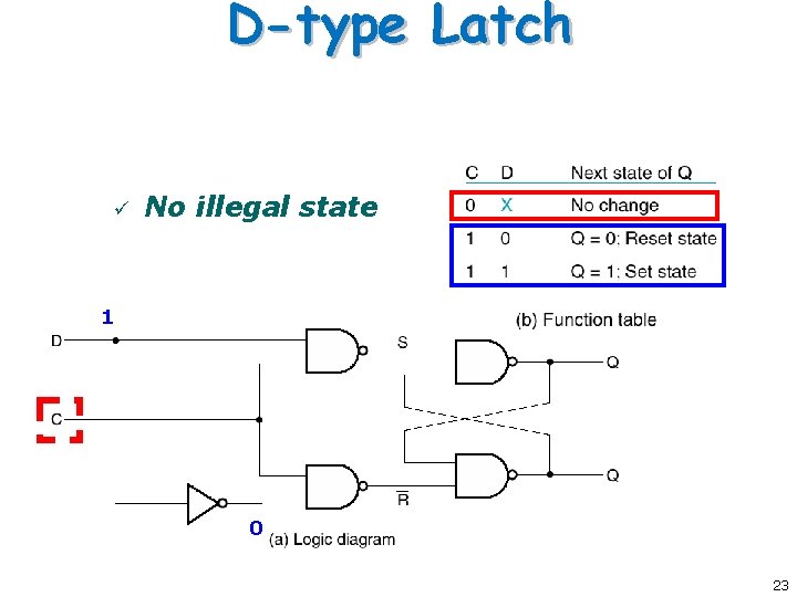
D-type Latch ü No illegal state 1 0 23
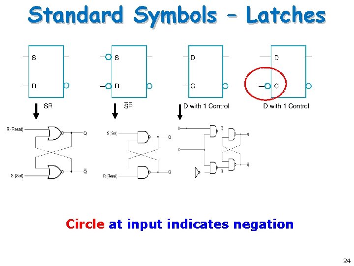
Standard Symbols – Latches Circle at input indicates negation 24
Issues with Latches
Transparency of Latches The state of a latch is allowed to switch by a momentary change in value on the control input. q L As long as C (the trigger ) is high, state can change! This is called transparency What is wrong with transparency? 26
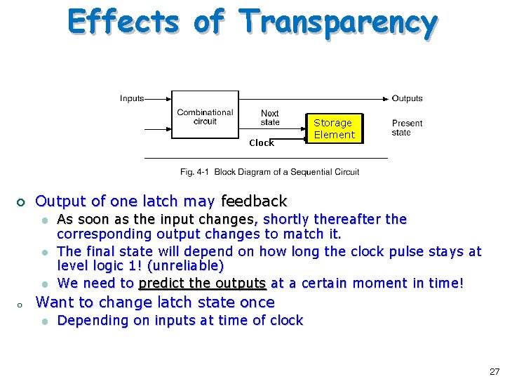
Effects of Transparency Clock ¡ Output of one latch may feedback l l l o Storage Element As soon as the input changes, shortly thereafter the corresponding output changes to match it. The final state will depend on how long the clock pulse stays at level logic 1! (unreliable) We need to predict the outputs at a certain moment in time! Want to change latch state once l Depending on inputs at time of clock 27
Flip Flops
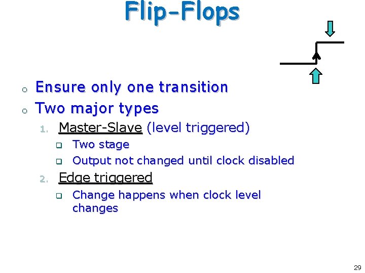
Flip-Flops o o Ensure only one transition Two major types 1. Master-Slave (level triggered) q q 2. Two stage Output not changed until clock disabled Edge triggered q Change happens when clock level changes 29
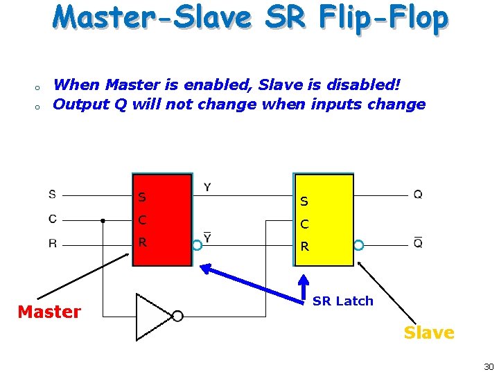
Master-Slave SR Flip-Flop o o When Master is enabled, Slave is disabled! Output Q will not change when inputs change Master S S C C R R SR Latch Slave 30
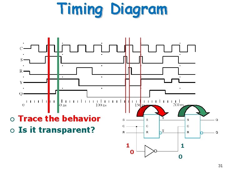
Timing Diagram ¡ ¡ Trace the behavior Is it transparent? 1 0 31
Have We Fixed the Problem? ¡ Output no longer transparent l l Combinational circuit can use last values New inputs appear at latches Not sent to output until clock low In one clock cycle we can predict what will happen 32
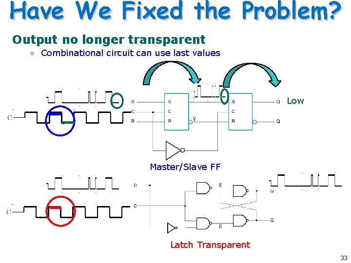
Have We Fixed the Problem? Output no longer transparent l Combinational circuit can use last values Low Master/Slave FF Latch Transparent 33
JK Flip Flops
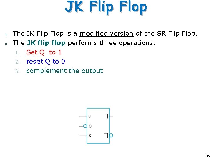
JK Flip Flop o o The JK Flip Flop is a modified version of the SR Flip Flop. The JK flip flop performs three operations: 1. Set Q to 1 2. reset Q to 0 3. complement the output 35
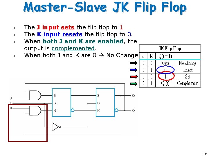
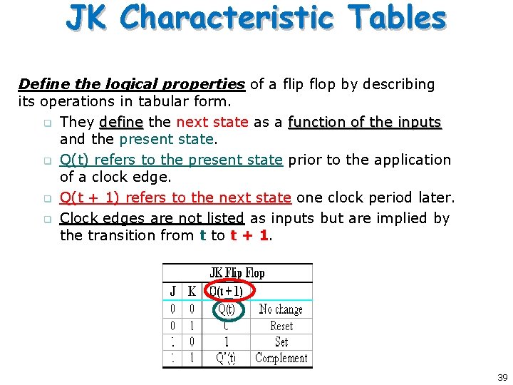
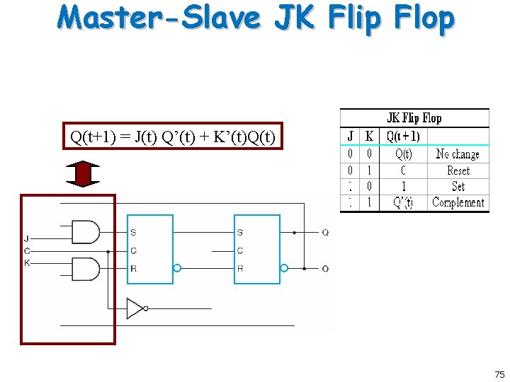
Master-Slave JK Flip Flop o o The J input sets the flip flop to 1. The K input resets the flip flop to 0. When both J and K are enabled, the output is complemented. When both J and K are 0 No Change 36
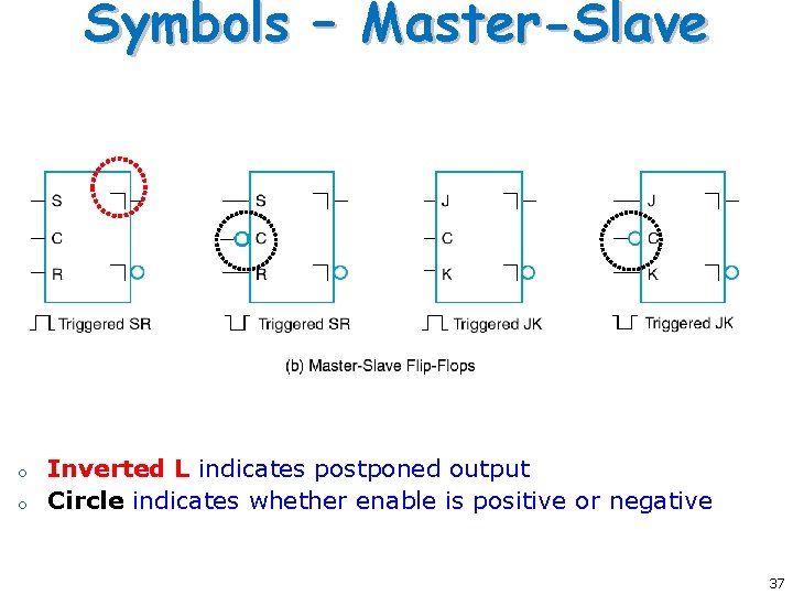
Symbols – Master-Slave o o Inverted L indicates postponed output Circle indicates whether enable is positive or negative 37
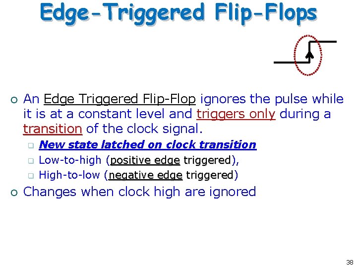
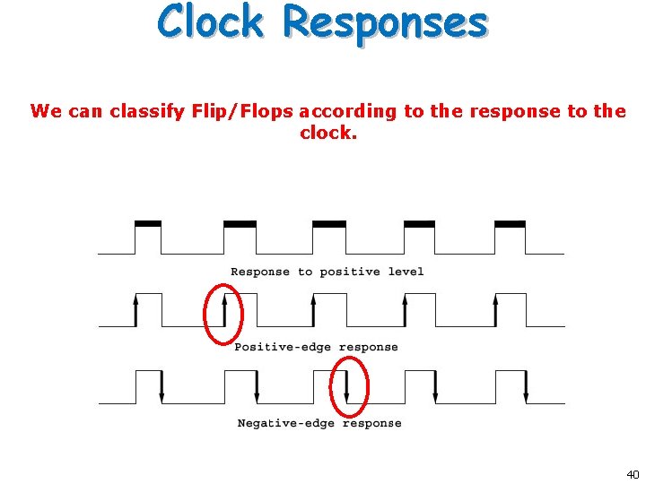
Edge-Triggered Flip-Flops ¡ An Edge Triggered Flip-Flop ignores the pulse while it is at a constant level and triggers only during a transition of the clock signal. q q q ¡ New state latched on clock transition Low-to-high (positive edge triggered), triggered High-to-low (negative edge triggered) triggered Changes when clock high are ignored 38
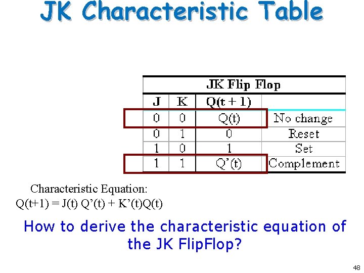
JK Characteristic Tables Define the logical properties of a flip flop by describing its operations in tabular form. q They define the next state as a function of the inputs and the present state. q Q(t) refers to the present state prior to the application of a clock edge. q Q(t + 1) refers to the next state one clock period later. q Clock edges are not listed as inputs but are implied by the transition from t to t + 1. 39
Clock Responses We can classify Flip/Flops according to the response to the clock. 40
D Flip Flops
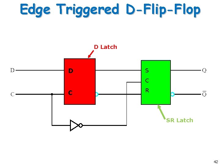
Edge Triggered D-Flip-Flop D Latch D S C C R SR Latch 42
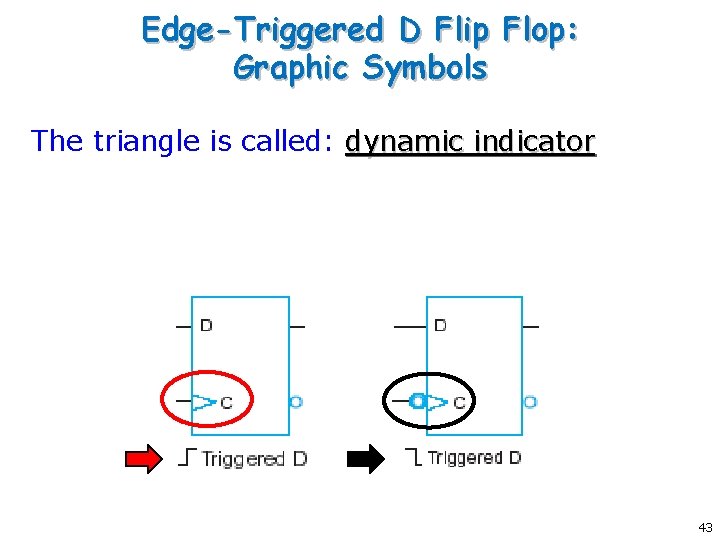
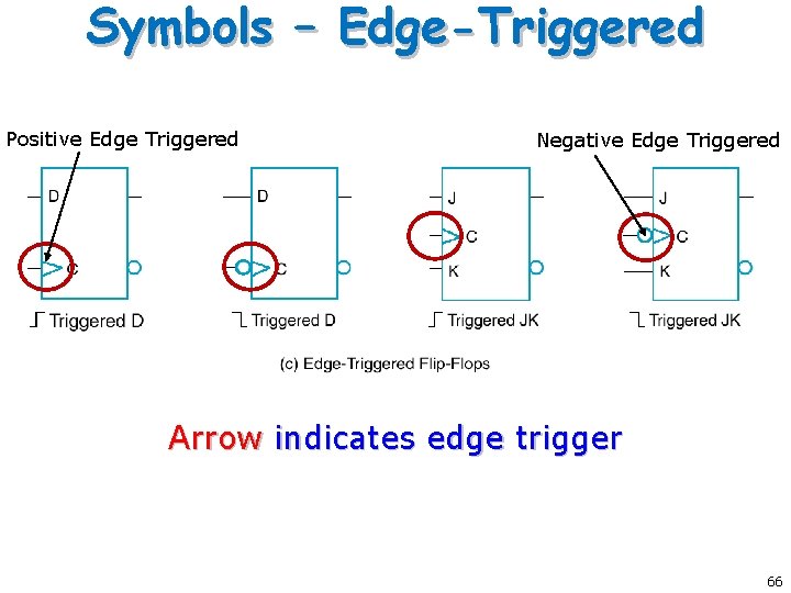
Edge-Triggered D Flip Flop: Graphic Symbols The triangle is called: dynamic indicator 43
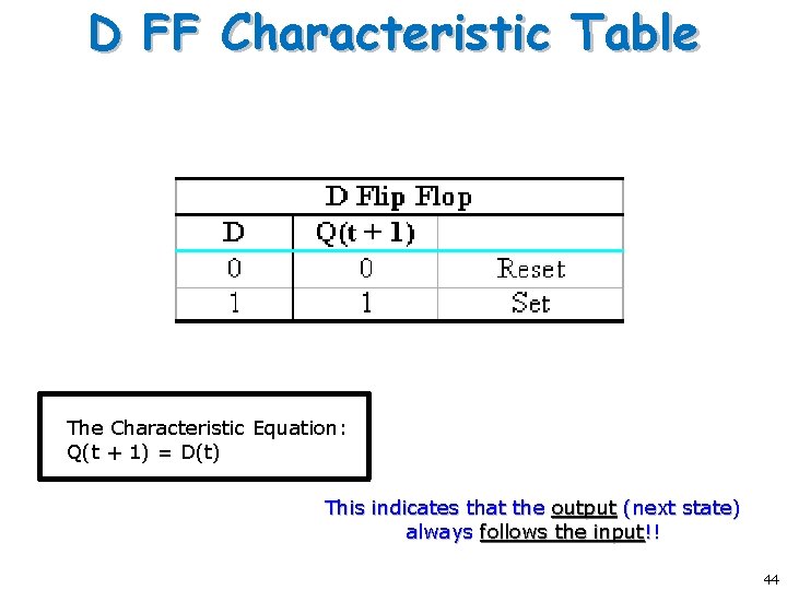
D FF Characteristic Table The Characteristic Equation: Q(t + 1) = D(t) This indicates that the output (next state) always follows the input!! 44
Other Flip Flops Other types of flip flops can be constructed by using the D flip flop and external logic. The two most commonly used are: 1. 2. Edge triggered JK flip flops T flip flops 45
Characteristic Tables
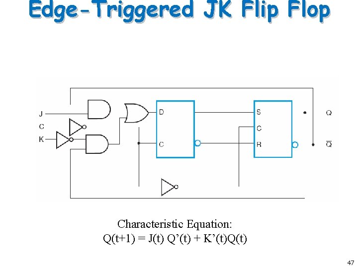
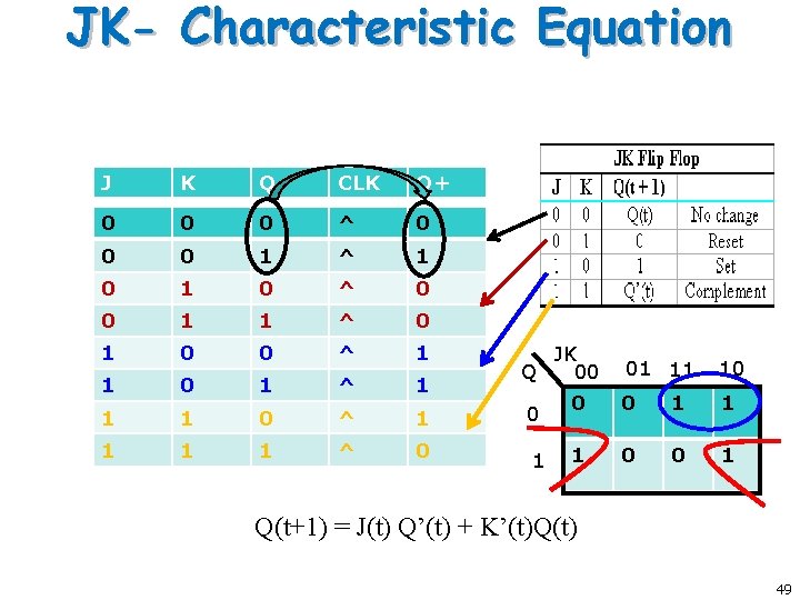
Edge-Triggered JK Flip Flop Characteristic Equation: Q(t+1) = J(t) Q’(t) + K’(t)Q(t) 47
JK Characteristic Table Characteristic Equation: Q(t+1) = J(t) Q’(t) + K’(t)Q(t) How to derive the characteristic equation of the JK Flip. Flop? 48
JK- Characteristic Equation J K Q CLK Q+ 0 0 0 ^ 0 0 0 1 ^ 1 0 ^ 0 0 1 1 ^ 0 1 0 0 ^ 1 1 0 1 ^ 1 1 1 0 ^ 1 1 ^ 0 JK Q 00 0 1 01 11 10 0 0 1 1 1 0 0 1 Q(t+1) = J(t) Q’(t) + K’(t)Q(t) 49
T-Flipflop
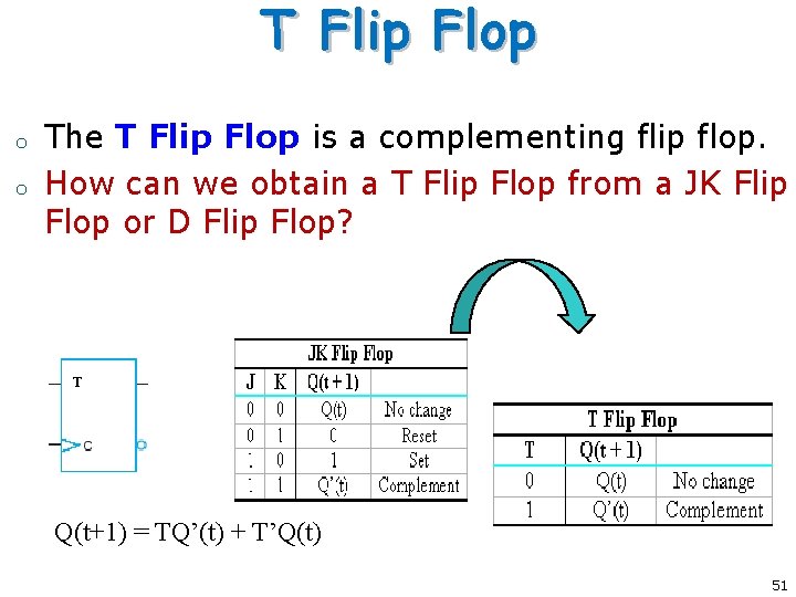
T Flip Flop o o The T Flip Flop is a complementing flip flop. How can we obtain a T Flip Flop from a JK Flip Flop or D Flip Flop? T Q(t+1) = TQ’(t) + T’Q(t) 51
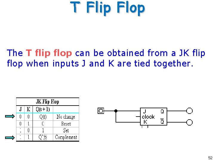
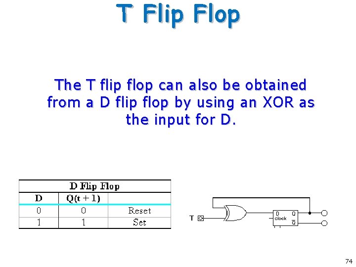
T Flip Flop The T flip flop can be obtained from a JK flip flop when inputs J and K are tied together. 52
Summary: Characteristic Equations
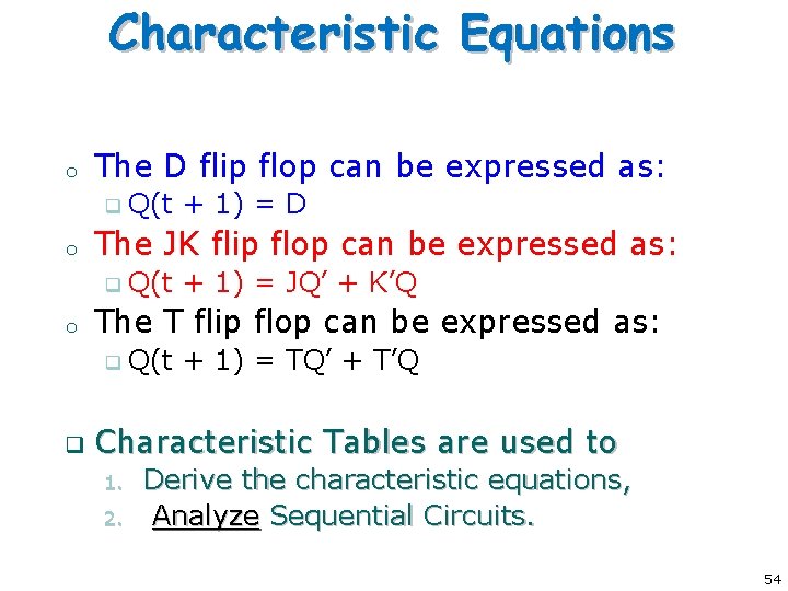
Characteristic Equations o The D flip flop can be expressed as: q o The JK flip flop can be expressed as: q o Q(t + 1) = JQ’ + K’Q The T flip flop can be expressed as: q q Q(t + 1) = D Q(t + 1) = TQ’ + T’Q Characteristic Tables are used to 1. 2. Derive the characteristic equations, Analyze Sequential Circuits. 54
Set/Reset Inputs
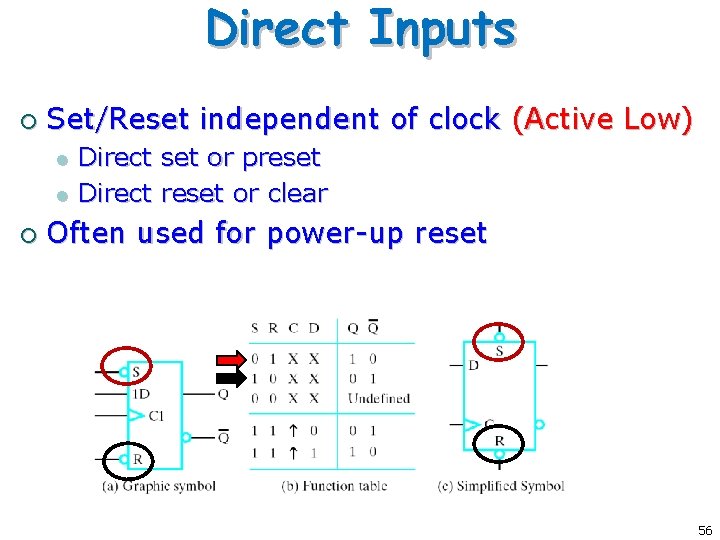
Direct Inputs ¡ Set/Reset independent of clock (Active Low) l l ¡ Direct set or preset Direct reset or clear Often used for power-up reset 56
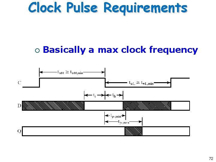
Timing
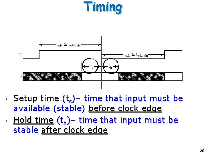
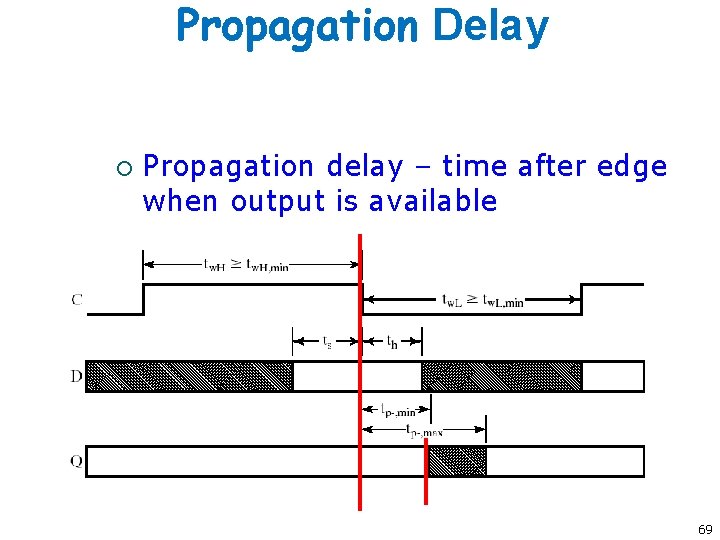
Timing • • Setup time (ts)– time that input must be available (stable) before clock edge Hold time (th)– time that input must be stable after clock edge 58
Sequential Circuits VHDL Code
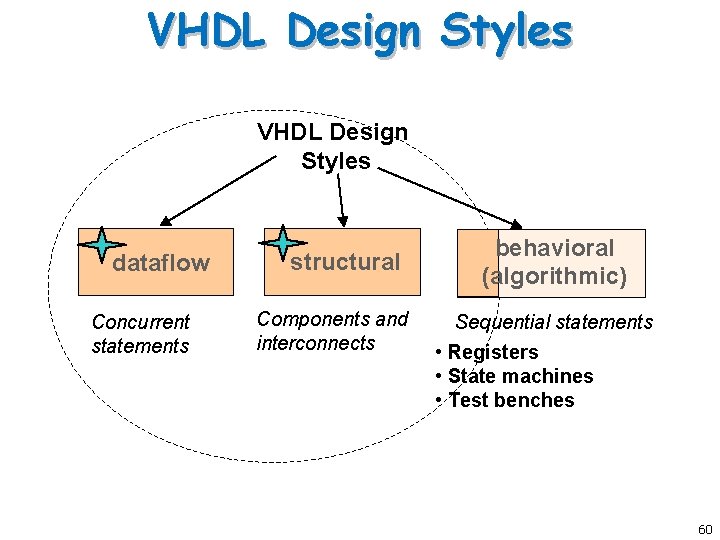
VHDL Design Styles dataflow Concurrent statements structural Components and interconnects behavioral (algorithmic) Sequential statements • Registers • State machines • Test benches 60
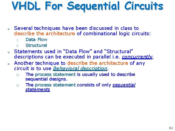
VHDL For Sequential Circuits o Several techniques have been discussed in class to describe the architecture of combinational logic circuits: 1. 2. o o Data Flow Structural Statements used in “Data Flow” and “Structural” descriptions can be executed in parallel i. e. concurrently. Another technique to describe the architecture of any circuit is to use Behavioral description. q q The process statement is usually used to describe sequential designs. The process statement consists of only sequential statements 61
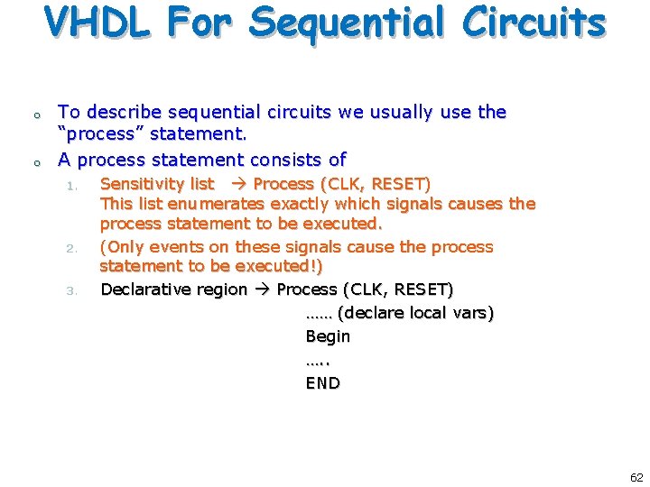
VHDL For Sequential Circuits o o To describe sequential circuits we usually use the “process” statement. A process statement consists of 1. 2. 3. Sensitivity list Process (CLK, RESET) This list enumerates exactly which signals causes the process statement to be executed. (Only events on these signals cause the process statement to be executed!) Declarative region Process (CLK, RESET) …… (declare local vars) Begin …. . END 62
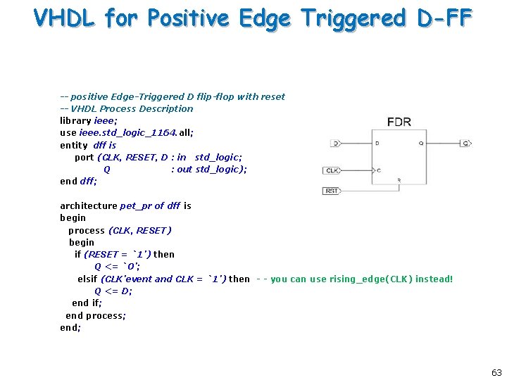
VHDL for Positive Edge Triggered D-FF -- positive Edge-Triggered D flip-flop with reset -- VHDL Process Description library ieee; use ieee. std_logic_1164. all; entity dff is port (CLK, RESET, D : in std_logic; Q : out std_logic); end dff; architecture pet_pr of dff is begin process (CLK, RESET) begin if (RESET = `1’) then Q <= `0’; elsif (CLK’event and CLK = `1’) then - - you can use rising_edge(CLK) instead! Q <= D; end if; end process; end; 63
Summary o o o Combinational logic are very interesting and useful for designing arithmetic circuits (adders, multipliers) or in other words the Data Path of a computer. Sequential circuits are capable of storing information between operations. They are useful in designing registers, counters, and CONTROL Circuits. Latches are storage elements that are asynchronous, transparent and are used to build more complex synchronous circuits such as Flip-Flops. Flip-flops avoid the transparency problem faced by latches and are either Master-Slave pulse active or edge triggered. Characteristic tables will be used to analyze the behavior of sequential circuits. 64
Symbols – Edge-Triggered Positive Edge Triggered Negative Edge Triggered Arrow indicates edge trigger 66
Comparison o Synchronous q q o Easier to analyze because can factor out gate delays Speed of the system is determined by the clock (maybe slowed!) Asynchronous q q Potentially faster Harder to analyze We will mainly look at synchronous 67
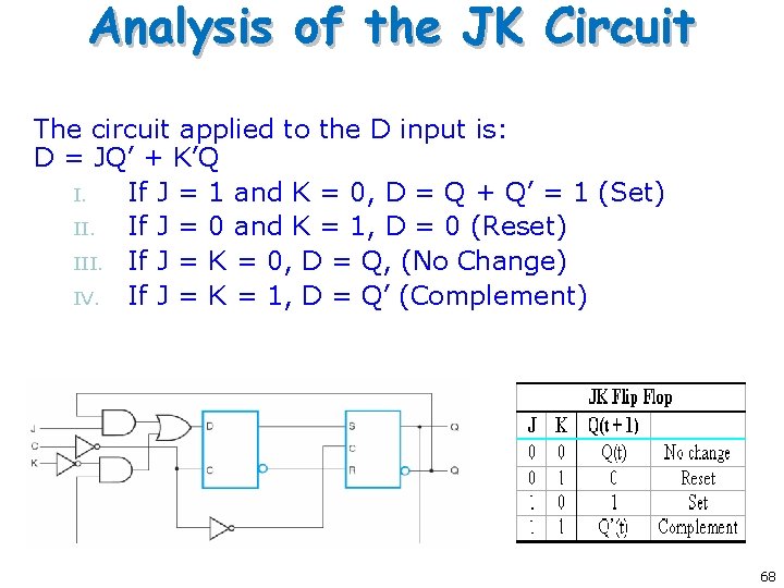
Analysis of the JK Circuit The circuit applied to the D input is: D = JQ’ + K’Q I. If J = 1 and K = 0, D = Q + Q’ = 1 (Set) II. If J = 0 and K = 1, D = 0 (Reset) III. If J = K = 0, D = Q, (No Change) IV. If J = K = 1, D = Q’ (Complement) 68
Propagation Delay ¡ Propagation delay – time after edge when output is available 69
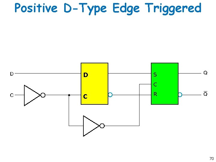
Positive D-Type Edge Triggered D S C C R 70
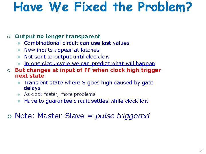
Have We Fixed the Problem? ¡ ¡ ¡ Output no longer transparent l Combinational circuit can use last values l New inputs appear at latches l Not sent to output until clock low l In one clock cycle we can predict what will happen But changes at input of FF when clock high trigger next state l Transient state where S goes high caused by gate delays l As clock faster, more problems l Have to guarantee circuit settles while clock low Note: Master-Slave = pulse triggered 71
Clock Pulse Requirements ¡ Basically a max clock frequency 72
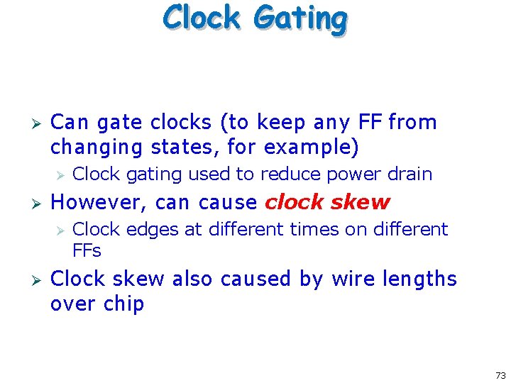
Clock Gating Ø Can gate clocks (to keep any FF from changing states, for example) Ø Ø However, can cause clock skew Ø Ø Clock gating used to reduce power drain Clock edges at different times on different FFs Clock skew also caused by wire lengths over chip 73
T Flip Flop The T flip flop can also be obtained from a D flip flop by using an XOR as the input for D. 74
Master-Slave JK Flip Flop Q(t+1) = J(t) Q’(t) + K’(t)Q(t) 75