Theory of ferromagnetic semiconductor Ga MnAs Tomas Jungwirth

- Slides: 37
Theory of ferromagnetic semiconductor (Ga, Mn)As Tomas Jungwirth Institute of Physics ASCR Jan Mašek, František Máca, Josef Kudrnovský, Alexandr Shick, Karel Výborný, Jan Zemen, Vít Novák, Kamil Olejník, et al. University of Nottingham Bryan Gallagher, Richard Campion, Tom Foxon, Kevin Edmonds, Andrew Rushforth, et al. Charles University, Prague Petr Němec, Petra Horodyská, Naďa Tesařová, Eva Rozkotová, et al. Hitachi Cambridge, Univ. Cambridge Jorg Wunderlich, Andrew Irvine, Elisa de Ranieri, Byonguk Park, et al. Texas A&M Jairo Sinova, et al. University of Texas Allan Ma. Donald, et al. H. Ohno, T. Dietl, M. Sawicki, C. Gould, L. Molenkamp, et al.
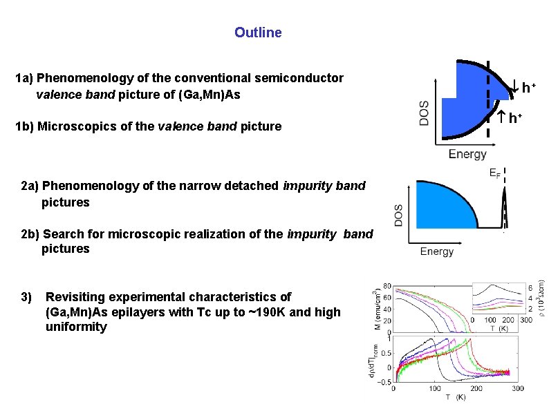
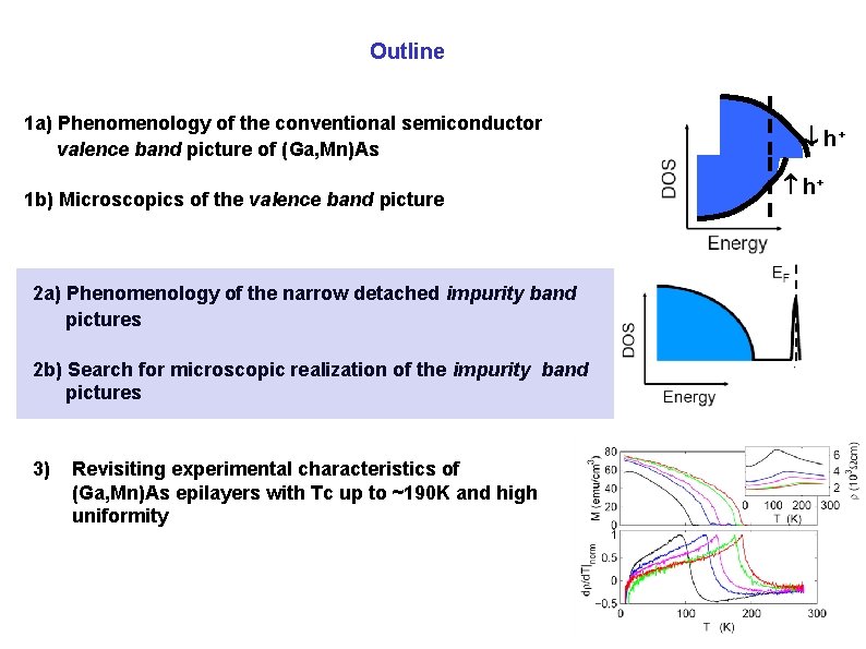
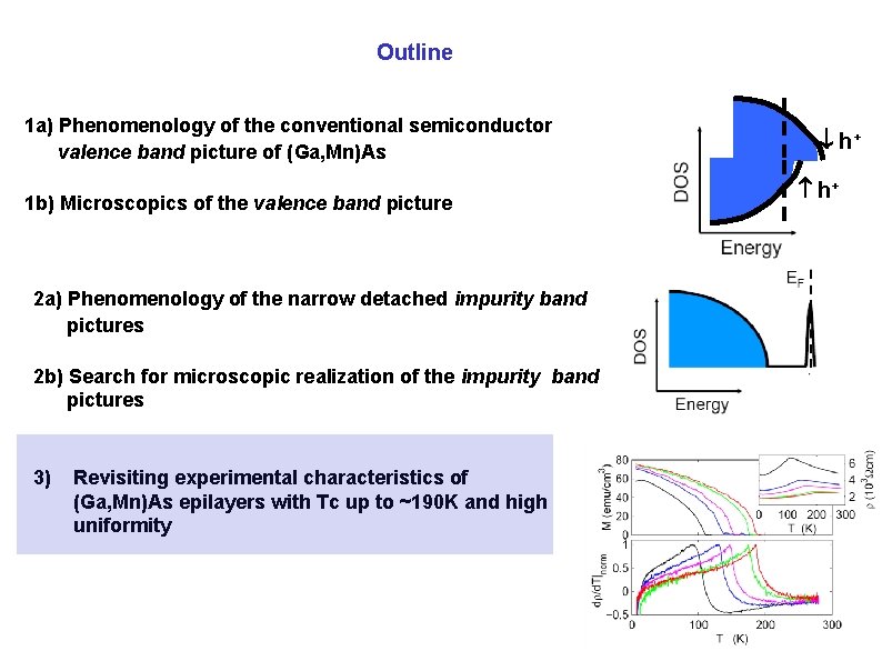
Outline 1 a) Phenomenology of the conventional semiconductor valence band picture of (Ga, Mn)As 1 b) Microscopics of the valence band picture 2 a) Phenomenology of the narrow detached impurity band pictures 2 b) Search for microscopic realization of the impurity band pictures 3) Revisiting experimental characteristics of (Ga, Mn)As epilayers with Tc up to ~190 K and high uniformity h+
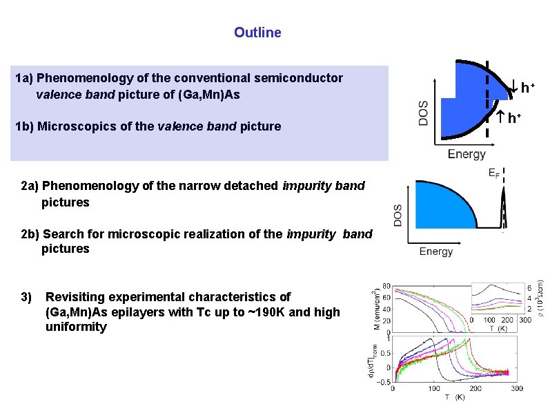
Outline 1 a) Phenomenology of the conventional semiconductor valence band picture of (Ga, Mn)As 1 b) Microscopics of the valence band picture 2 a) Phenomenology of the narrow detached impurity band pictures 2 b) Search for microscopic realization of the impurity band pictures 3) Revisiting experimental characteristics of (Ga, Mn)As epilayers with Tc up to ~190 K and high uniformity h+
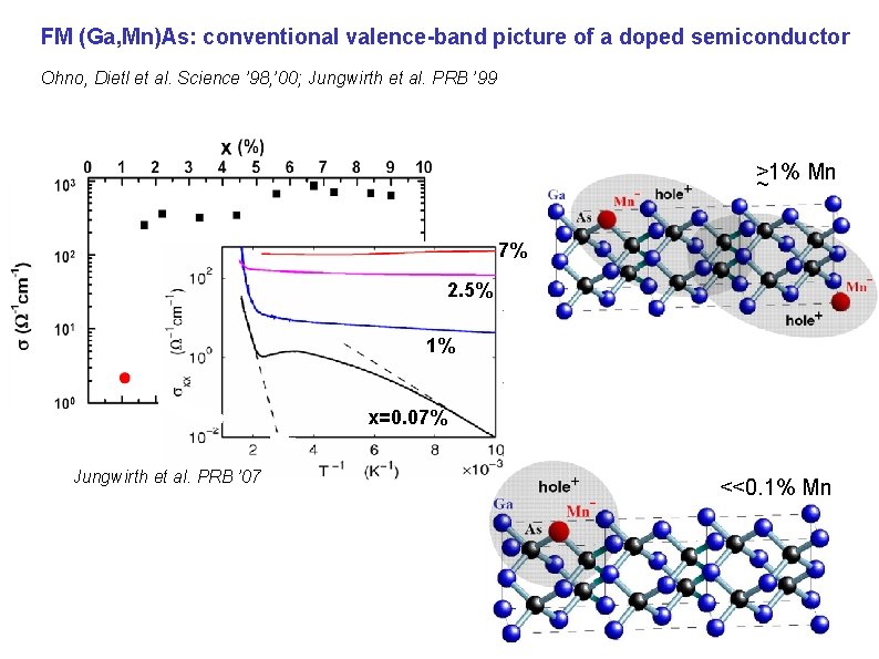
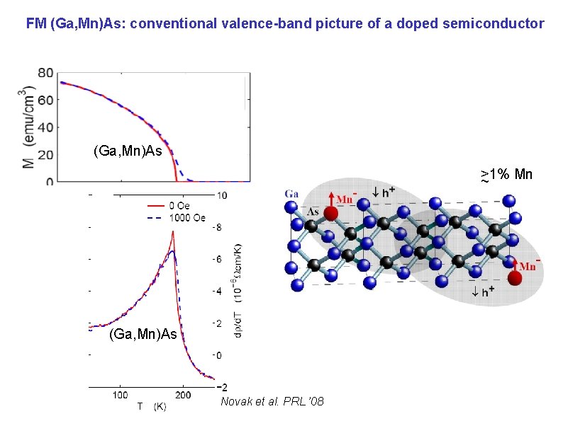
FM (Ga, Mn)As: conventional valence-band picture of a doped semiconductor Ohno, Dietl et al. Science ’ 98, ’ 00; Jungwirth et al. PRB ’ 99 >1% Mn ~ 7% 2. 5% 1% x=0. 07% Jungwirth et al. PRB ’ 07 <<0. 1% Mn
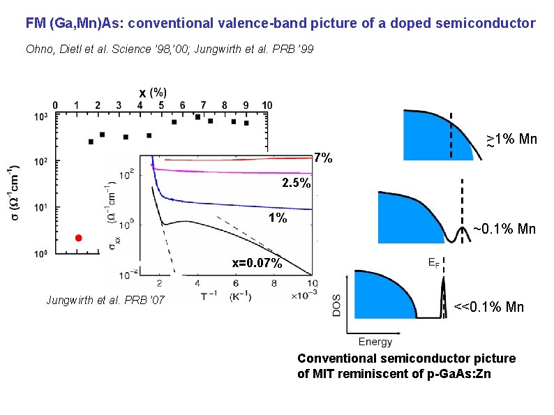
FM (Ga, Mn)As: conventional valence-band picture of a doped semiconductor Ohno, Dietl et al. Science ’ 98, ’ 00; Jungwirth et al. PRB ’ 99 7% >1% Mn ~ 2. 5% 1% ~0. 1% Mn x=0. 07% Jungwirth et al. PRB ’ 07 <<0. 1% Mn Conventional semiconductor picture of MIT reminiscent of p-Ga. As: Zn
FM (Ga, Mn)As: conventional valence-band picture of a doped semiconductor (Ga, Mn)As >1% Mn ~ (Ga, Mn)As Novak et al. PRL ’ 08
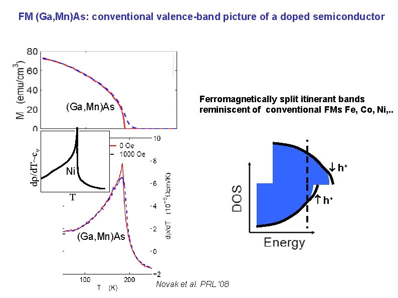
FM (Ga, Mn)As: conventional valence-band picture of a doped semiconductor d /d. T~cv (Ga, Mn)As Ferromagnetically split itinerant bands reminiscent of conventional FMs Fe, Co, Ni, . . h+ Ni T h+ (Ga, Mn)As Novak et al. PRL ’ 08
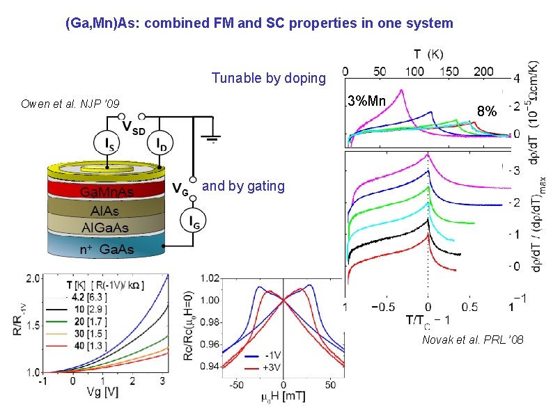
(Ga, Mn)As: combined FM and SC properties in one system Tunable by doping 3%Mn Owen et al. NJP ’ 09 8% and by gating Novak et al. PRL ’ 08
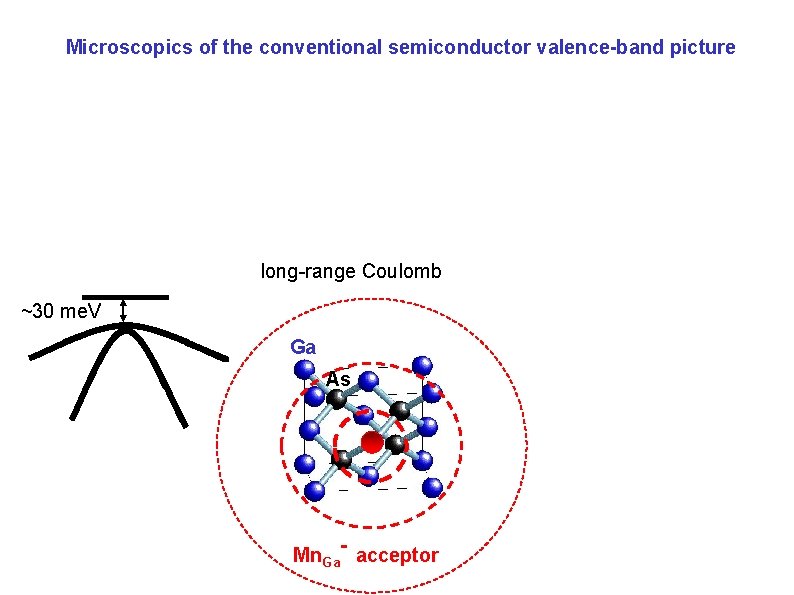
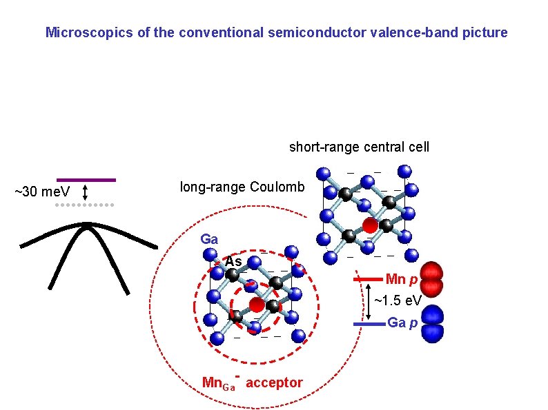
Microscopics of the conventional semiconductor valence-band picture long-range Coulomb ~30 me. V Ga As Mn. Ga- acceptor
Microscopics of the conventional semiconductor valence-band picture short-range central cell ~30 me. V long-range Coulomb Ga As Mn p ~1. 5 e. V Ga p Mn. Ga- acceptor
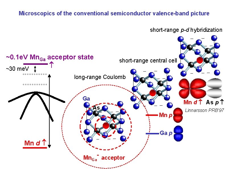
Microscopics of the conventional semiconductor valence-band picture short-range p-d hybridization ~0. 1 e. V Mn. Ga acceptor state ~30 me. V short-range central cell long-range Coulomb Ga Mn d As p As Mn p Ga p Mn d Mn. Ga- acceptor Linnarsson PRB’ 97
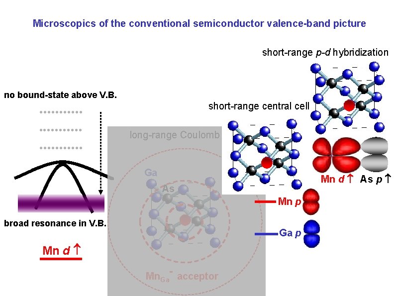
Microscopics of the conventional semiconductor valence-band picture short-range p-d hybridization no bound-state above V. B. short-range central cell long-range Coulomb Ga Mn d As p As Mn p broad resonance in V. B. Ga p Mn d Mn. Ga- acceptor
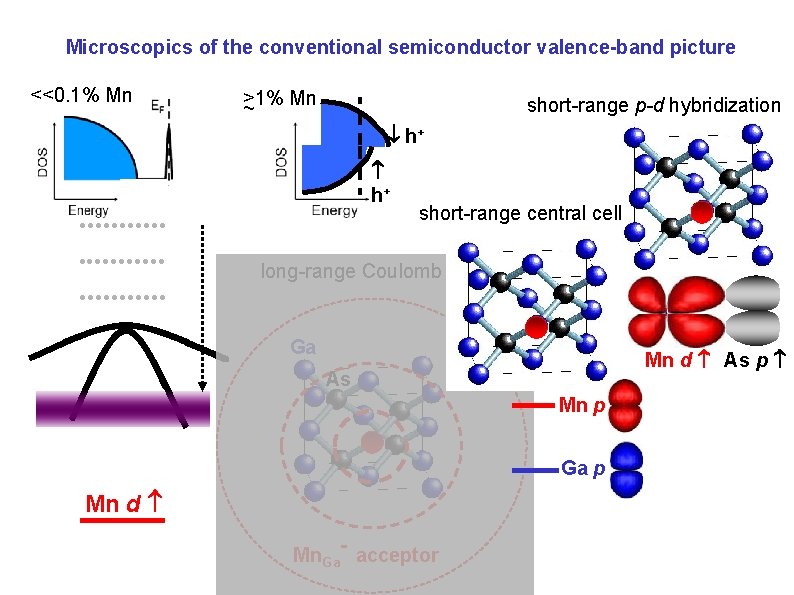
Microscopics of the conventional semiconductor valence-band picture <<0. 1% Mn >1% Mn ~ short-range p-d hybridization h+ short-range central cell long-range Coulomb Ga Mn d As p As Mn p Ga p Mn d Mn. Ga- acceptor
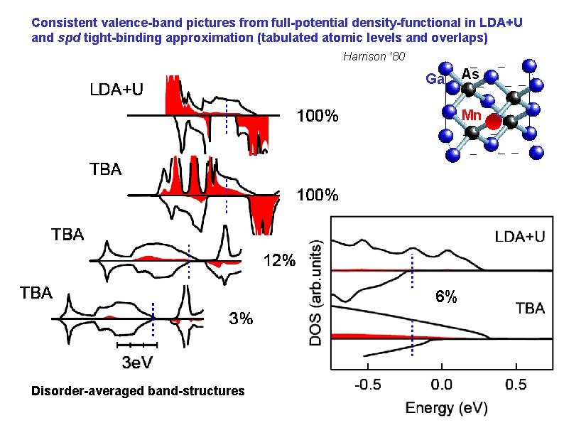
Consistent valence-band pictures from full-potential density-functional in LDA+U and spd tight-binding approximation (tabulated atomic levels and overlaps) Harrison ‘ 80 Ga As Mn 6% Disorder-averaged band-structures
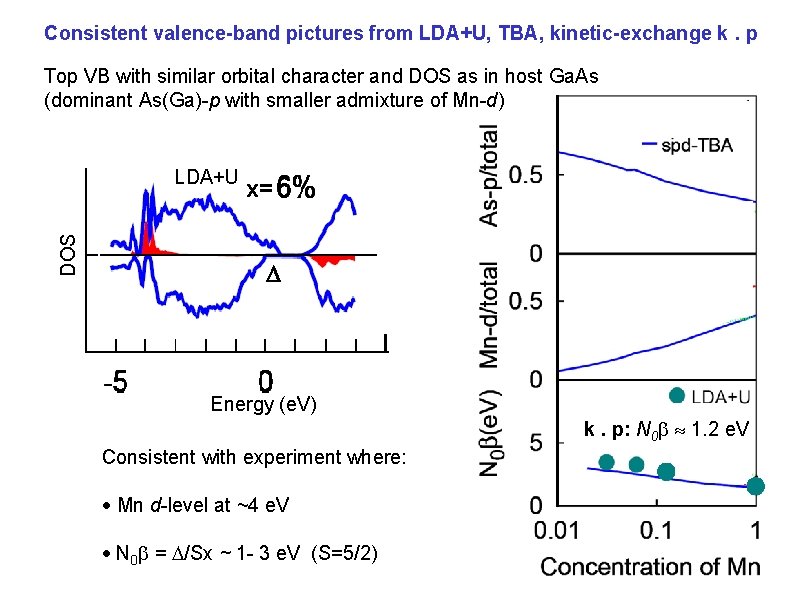
Consistent valence-band pictures from LDA+U, TBA, kinetic-exchange k. p Top VB with similar orbital character and DOS as in host Ga. As (dominant As(Ga)-p with smaller admixture of Mn-d) DOS LDA+U x= Energy (e. V) k. p: N 0 1. 2 e. V Consistent with experiment where: Mn d-level at ~4 e. V N 0 = /Sx ~ 1 - 3 e. V (S=5/2)
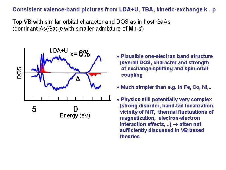
Consistent valence-band pictures from LDA+U, TBA, kinetic-exchange k. p Top VB with similar orbital character and DOS as in host Ga. As (dominant As(Ga)-p with smaller admixture of Mn-d) DOS LDA+U x= Plausible one-electron band structure (overall DOS, character and strength of exchange-splitting and spin-orbit coupling Much simpler than e. g. in Fe, Co, Ni, . . Energy (e. V) Physics still potentially very complex (strong disorder, band-tail localization, vicinity of MIT, thermal fluctuations of magnetization, electron-electron interaction effects, . . ) often not sufficiently discussed in VB based theories
Outline 1 a) Phenomenology of the conventional semiconductor valence band picture of (Ga, Mn)As 1 b) Microscopics of the valence band picture 2 a) Phenomenology of the narrow detached impurity band pictures 2 b) Search for microscopic realization of the impurity band pictures 3) Revisiting experimental characteristics of (Ga, Mn)As epilayers with Tc up to ~190 K and high uniformity h+
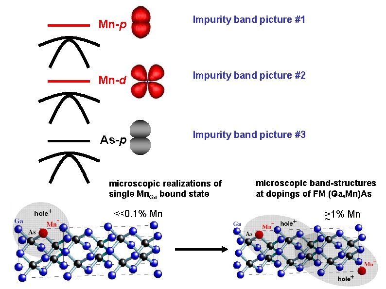
Mn-p Impurity band picture #1 Mn-d Impurity band picture #2 As-p Impurity band picture #3 microscopic realizations of single Mn. Ga bound state <<0. 1% Mn microscopic band-structures at dopings of FM (Ga, Mn)As >1% Mn ~
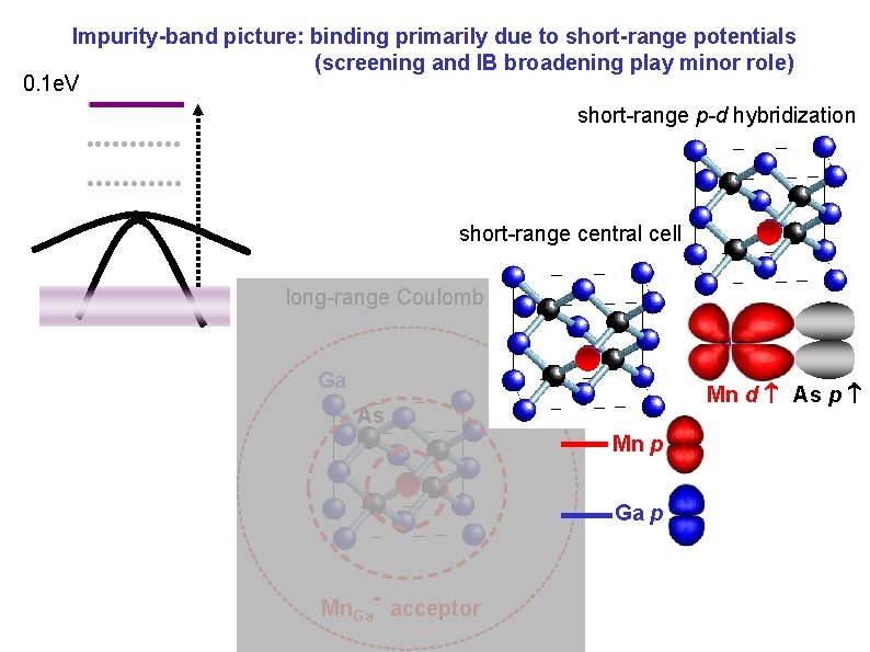
Impurity-band picture: binding primarily due to short-range potentials (screening and IB broadening play minor role) 0. 1 e. V short-range p-d hybridization short-range central cell long-range Coulomb Ga Mn d As p As Mn p Ga p Mn. Ga- acceptor
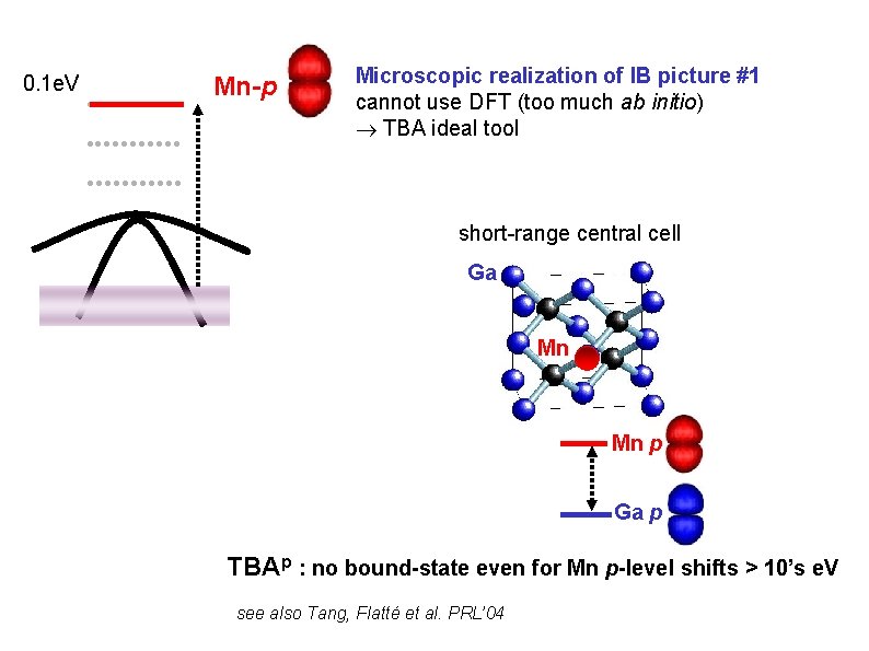
0. 1 e. V Mn-p Microscopic realization of IB picture #1 cannot use DFT (too much ab initio) TBA ideal tool short-range central cell Ga Mn Mn p Ga p TBAp : no bound-state even for Mn p-level shifts > 10’s e. V see also Tang, Flatté et al. PRL’ 04
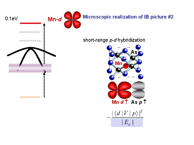
0. 1 e. V Mn-d Microscopic realization of IB picture #2 short-range p-d hybridization As Mn Mn d As p
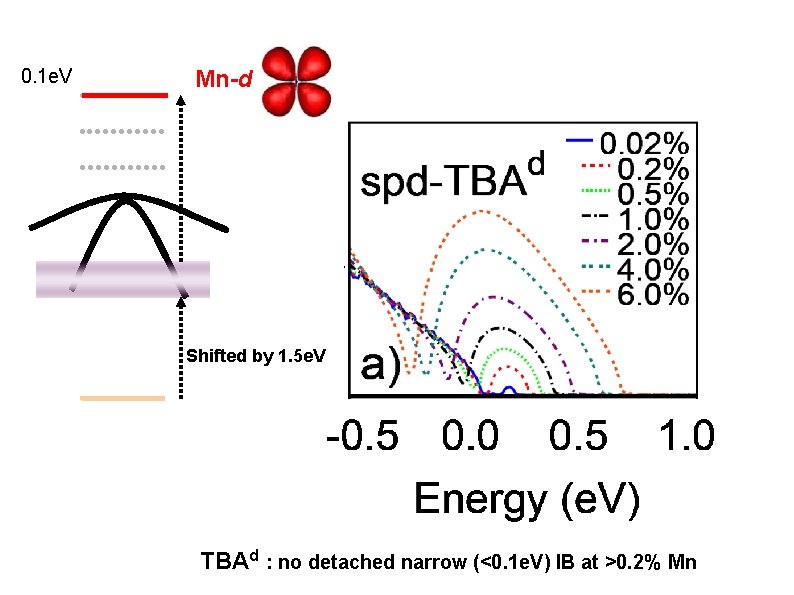
0. 1 e. V Mn-d Shifted by 1. 5 e. V TBAd : no detached narrow (<0. 1 e. V) IB at >0. 2% Mn
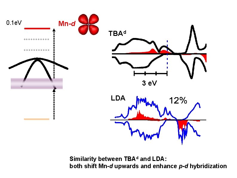
0. 1 e. V Mn-d TBAd 3 e. V LDA Similarity between TBAd and LDA: both shift Mn-d upwards and enhance p-d hybridization
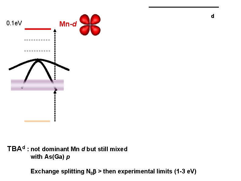
d 0. 1 e. V Mn-d TBAd : not dominant Mn d but still mixed with As(Ga) p Exchange splitting N 0 > then experimental limits (1 -3 e. V)
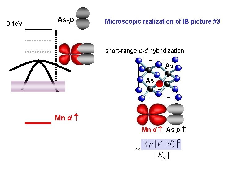
0. 1 e. V As-p Microscopic realization of IB picture #3 short-range p-d hybridization As As Mn d As p
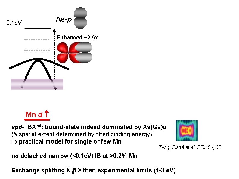
As-p 0. 1 e. V Enhanced ~2. 5 x Mn d spd-TBApd: bound-state indeed dominated by As(Ga)p (& spatial extent determined by fitted binding energy) practical model for single or few Mn Tang, Flatté et al. PRL’ 04, ’ 05 no detached narrow (<0. 1 e. V) IB at >0. 2% Mn Exchange splitting N 0 > then experimental limits (1 -3 e. V)
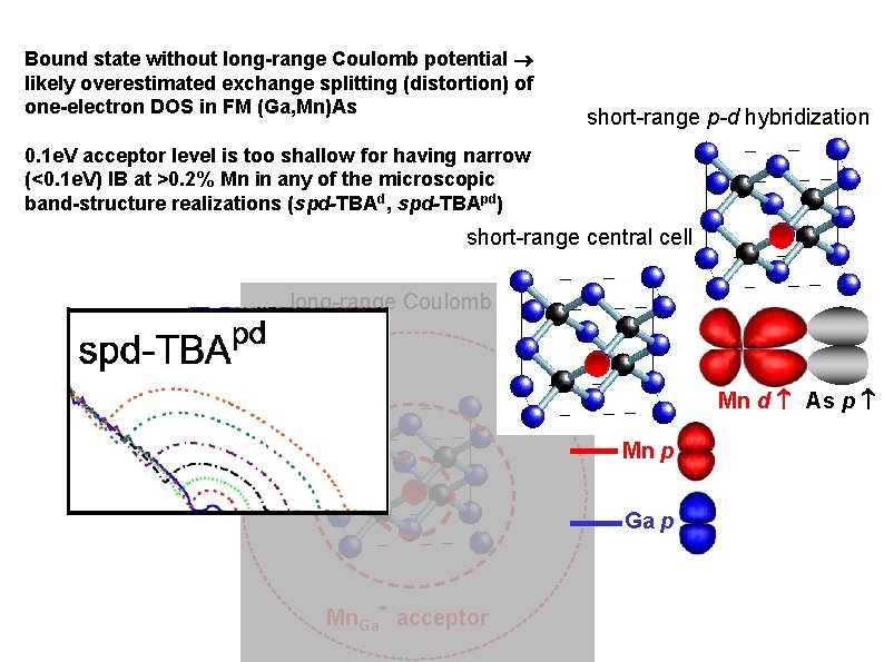
Bound state without long-range Coulomb potential likely overestimated exchange splitting (distortion) of one-electron DOS in FM (Ga, Mn)As short-range p-d hybridization 0. 1 e. V acceptor level is too shallow for having narrow (<0. 1 e. V) IB at >0. 2% Mn in any of the microscopic band-structure realizations (spd-TBAd, spd-TBApd) short-range central cell long-range Coulomb Ga Mn d As p As Mn p Ga p Mn. Ga- acceptor
Outline 1 a) Phenomenology of the conventional semiconductor valence band picture of (Ga, Mn)As 1 b) Microscopics of the valence band picture 2 a) Phenomenology of the narrow detached impurity band pictures 2 b) Search for microscopic realization of the impurity band pictures 3) Revisiting experimental characteristics of (Ga, Mn)As epilayers with Tc up to ~190 K and high uniformity h+
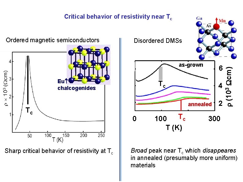
Critical behavior of resistivity near Tc Disordered DMSs as-grown Eu chalcogenides Tc Sharp critical behavior of resistivity at Tc 6 Tc 4 annealed 0 Tc 100 T (K) 2 (103 cm) Ordered magnetic semiconductors 300 Broad peak near Tc which disappeares in annealed (presumably more uniform) materials
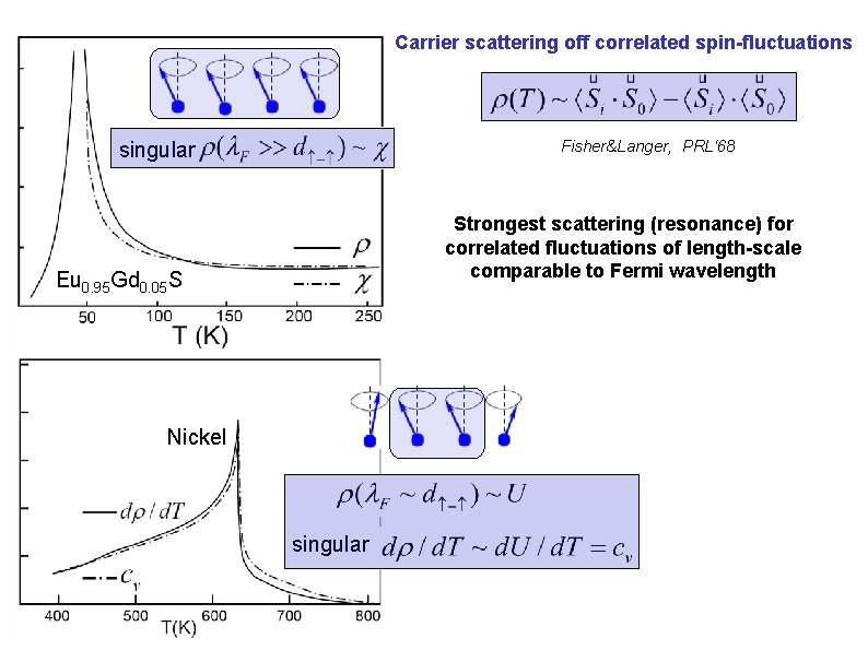
Carrier scattering off correlated spin-fluctuations Fisher&Langer, PRL‘ 68 singular Strongest scattering (resonance) for correlated fluctuations of length-scale comparable to Fermi wavelength Eu 0. 95 Gd 0. 05 S Nickel singular
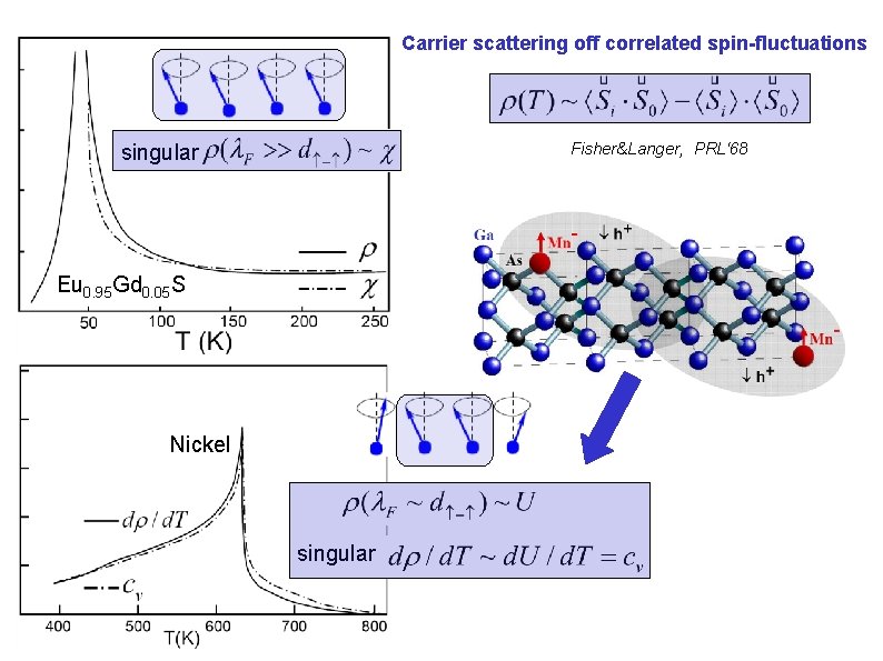
Carrier scattering off correlated spin-fluctuations Fisher&Langer, PRL‘ 68 singular Eu 0. 95 Gd 0. 05 S Nickel singular
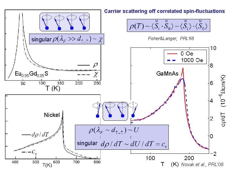
Carrier scattering off correlated spin-fluctuations Fisher&Langer, PRL‘ 68 singular Eu 0. 95 Gd 0. 05 S Ga. Mn. As Nickel singular Novak et al. , PRL‘ 08
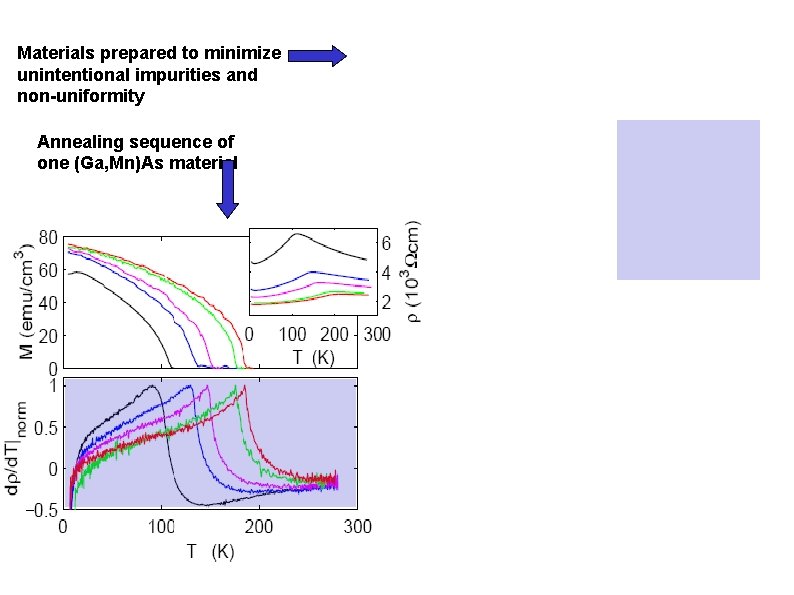
Materials prepared to minimize unintentional impurities and non-uniformity
Materials prepared to minimize unintentional impurities and non-uniformity Annealing sequence of one (Ga, Mn)As material
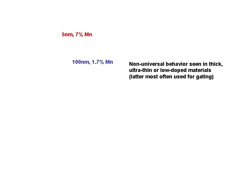
5 nm, 7% Mn 100 nm, 1. 7% Mn Non-universal behavior seen in thick, ultra-thin or low-doped materials (latter most often used for gating)
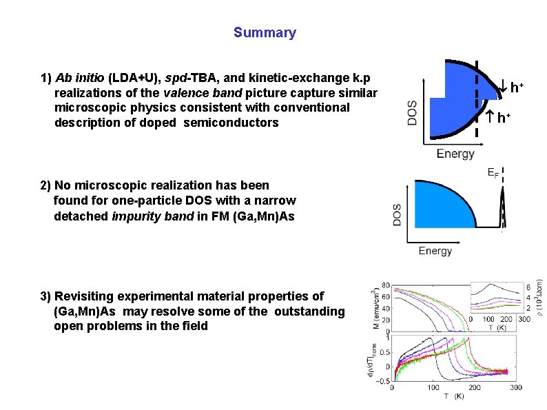
Summary 1) Ab initio (LDA+U), spd-TBA, and kinetic-exchange k. p realizations of the valence band picture capture similar microscopic physics consistent with conventional description of doped semiconductors 2) No microscopic realization has been found for one-particle DOS with a narrow detached impurity band in FM (Ga, Mn)As 3) Revisiting experimental material properties of (Ga, Mn)As may resolve some of the outstanding open problems in the field h+