USING SPIN IN FUTURE ELECTRONIC DEVICES Tomas Jungwirth












- Slides: 48
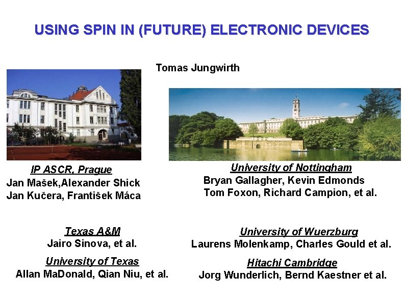
USING SPIN IN (FUTURE) ELECTRONIC DEVICES Tomas Jungwirth IP ASCR, Prague Jan Mašek, Alexander Shick Jan Kučera, František Máca University of Nottingham Bryan Gallagher, Kevin Edmonds Tom Foxon, Richard Campion, et al. Texas A&M Jairo Sinova, et al. University of Wuerzburg Laurens Molenkamp, Charles Gould et al. University of Texas Allan Ma. Donald, Qian Niu, et al. Hitachi Cambridge Jorg Wunderlich, Bernd Kaestner et al.
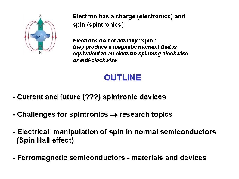
Electron has a charge (electronics) and spin (spintronics) Electrons do not actually “spin”, they produce a magnetic moment that is equivalent to an electron spinning clockwise or anti-clockwise OUTLINE - Current and future (? ? ? ) spintronic devices - Challenges for spintronics research topics - Electrical manipulation of spin in normal semiconductors (Spin Hall effect) - Ferromagnetic semiconductors - materials and devices
CURRENT SPINTRONIC DEVICES
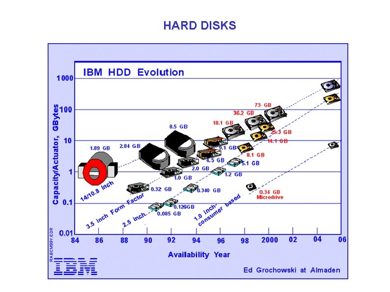
HARD DISKS
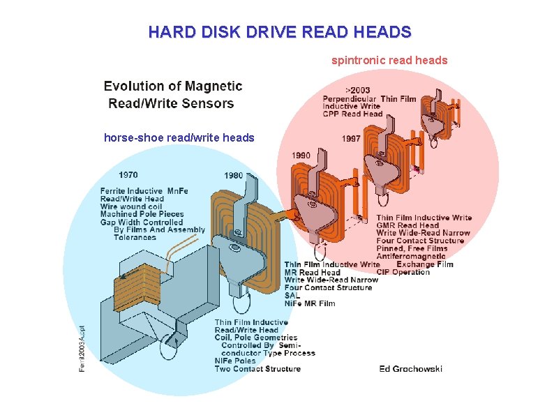
HARD DISK DRIVE READ HEADS spintronic read heads horse-shoe read/write heads
Anisotropic magnetoresistance (AMR) read head 1992 - dawn of spintronics Ferromagnetism large response (many spins) to small magnetic fields Spin-orbit coupling spin response detected electrically
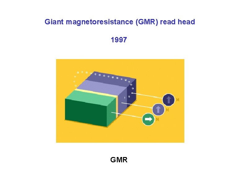
Giant magnetoresistance (GMR) read head 1997 GMR
. MEMORY CHIPS DRAM (capacitor) - high density, cheep x slow, cheep high power, volatile . SRAM (transistors) - low power, fast x low density, fast expensive, volatile . Flash (floating gate) - non-volatile x slow, limited life, expensive Operation through electron charge manipulation
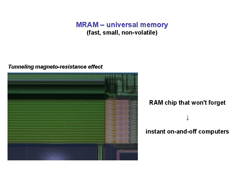
MRAM – universal memory (fast, small, non-volatile) Tunneling magneto-resistance effect RAM chip that won't forget ↓ instant on-and-off computers
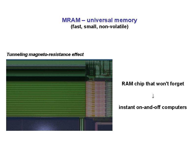
MRAM – universal memory (fast, small, non-volatile) Tunneling magneto-resistance effect RAM chip that won't forget ↓ instant on-and-off computers
FUTURE (? or ? ? ? ) SPINTRONIC DEVICES
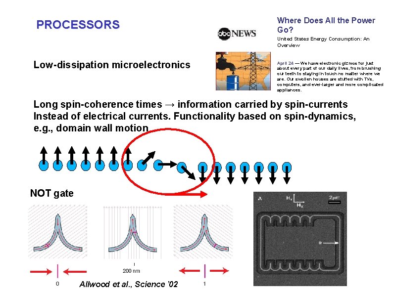
PROCESSORS Low-dissipation microelectronics Where Does All the Power Go? The power we use at home and outside of work accounts for only about a fifth of the total energy consumed in the United States every year, according to the Department of Energy. (ABCNEWS. com) United States Energy Consumption: An Overview April 24 — We have electronic gizmos for just about every part of our daily lives, from brushing our teeth to staying in touch no matter where we are. Our swollen houses are stuffed with TVs, computers, and ever-larger and more complicated appliances. Long spin-coherence times → information carried by spin-currents Instead of electrical currents. Functionality based on spin-dynamics, e. g. , domain wall motion NOT gate Allwood et al. , Science ’ 02
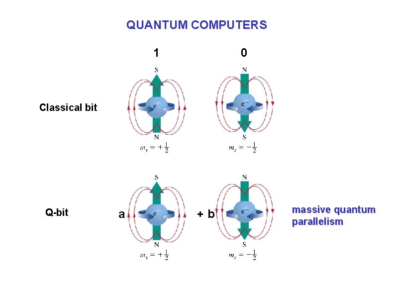
QUANTUM COMPUTERS 1 0 Classical bit Q-bit a +b massive quantum parallelism
CHALLENGES FOR SPINTRONICS
EXANGE-BIAS FM AFM fails when scaled down to ~10 nm dimensions Look for other MR concepts
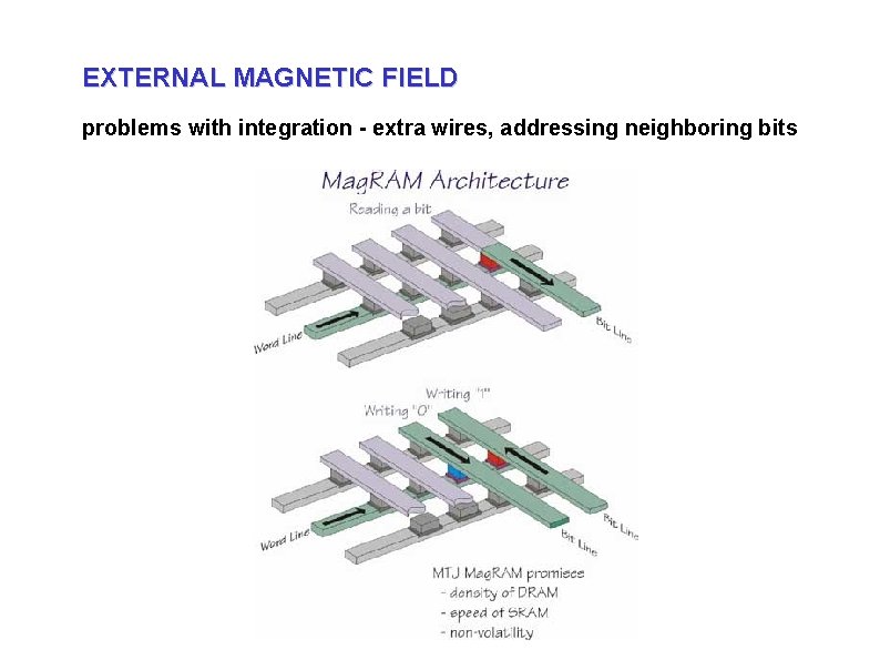
EXTERNAL MAGNETIC FIELD problems with integration - extra wires, addressing neighboring bits
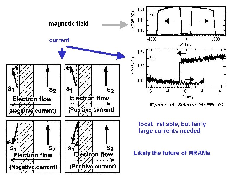
Current (insted of magnetic field) induced switching Buhrman & Ralph, NNUN ABSTRACTS '02 Slonczewski, JMMM '96; Berger, PRB '96 Angular momentum conservation spin-torque
magnetic field current Myers et al. , Science '99; PRL '02 local, reliable, but fairly large currents needed Likely the future of MRAMs
INTEGRATION WITH SEMICONDUCTOR ELECTRONICS �Spin-valve transistor �Metal ferromagnet to semiconductor spin-injector �All-semiconductor spintronics - electrical manipulation of spins (no external magnetic field) - making semiconductors ferromagnetic
ELECTRICAL MANIPULATION OF SPINS IN NORMAL SEMICONDUCTORS - SPIN HALL EFFECT
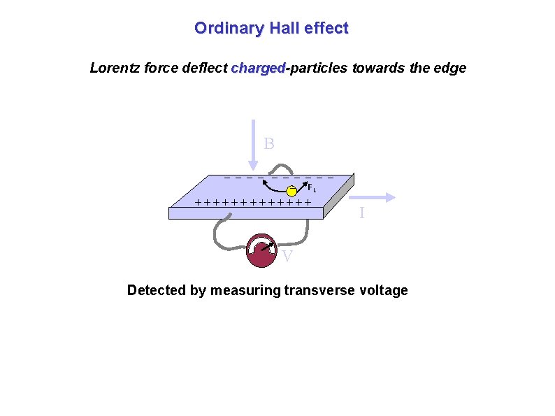
Ordinary Hall effect Lorentz force deflect charged-particles towards the edge B _ _ _ FL +++++++ I V Detected by measuring transverse voltage
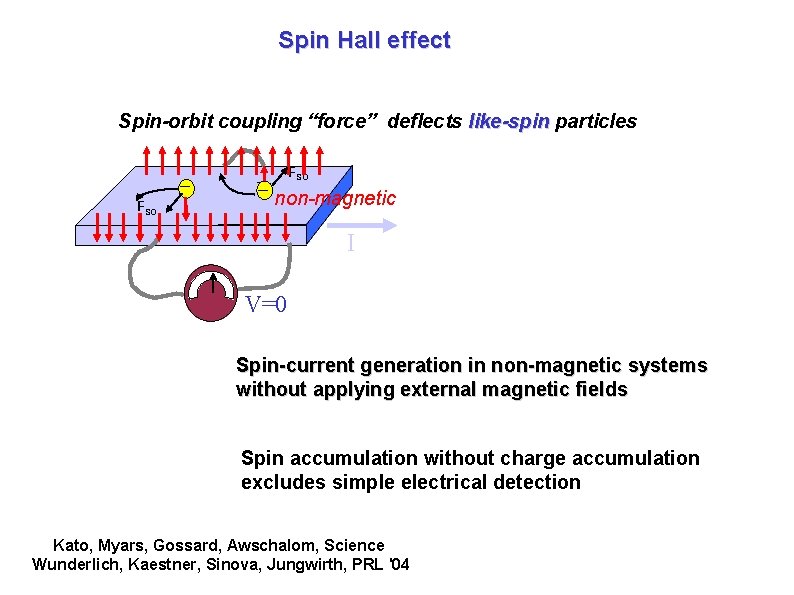
Spin Hall effect Spin-orbit coupling “force” deflects like-spin particles _ FSO __ FSO non-magnetic I V=0 Spin-current generation in non-magnetic systems without applying external magnetic fields Spin accumulation without charge accumulation excludes simple electrical detection Kato, Myars, Gossard, Awschalom, Science Wunderlich, Kaestner, Sinova, Jungwirth, PRL '04
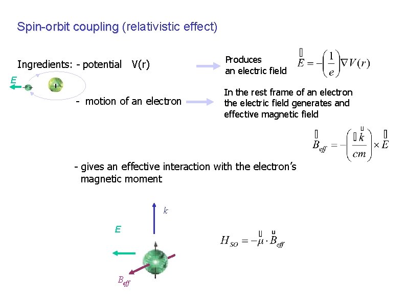
Spin-orbit coupling (relativistic effect) Spin-orbit coupling Produces an electric field Ingredients: - potential V(r) E - motion of an electron In the rest frame of an electron the electric field generates and effective magnetic field - gives an effective interaction with the electron’s magnetic moment k E Beff
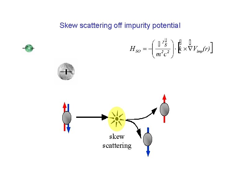
Skew scattering off impurity potential skew scattering
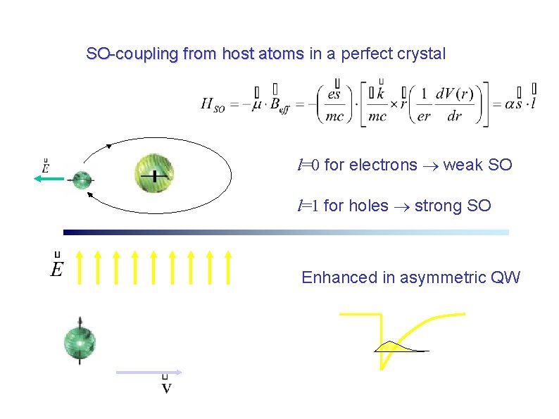
SO-coupling from host atoms in a perfect crystal SO-coupling from host atoms l=0 for electrons weak SO l=1 for holes strong SO Enhanced in asymmetric QW
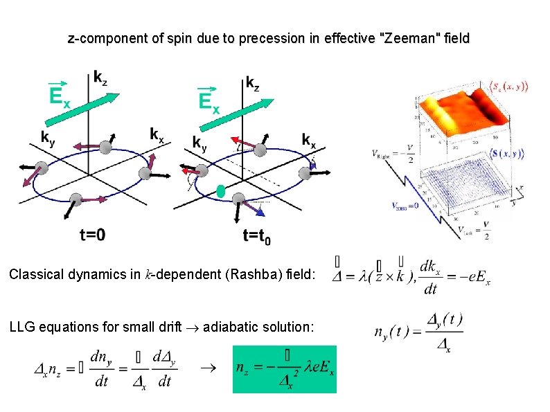
z-component of spin due to precession in effective "Zeeman" field Classical dynamics in k-dependent (Rashba) field: LLG equations for small drift adiabatic solution:
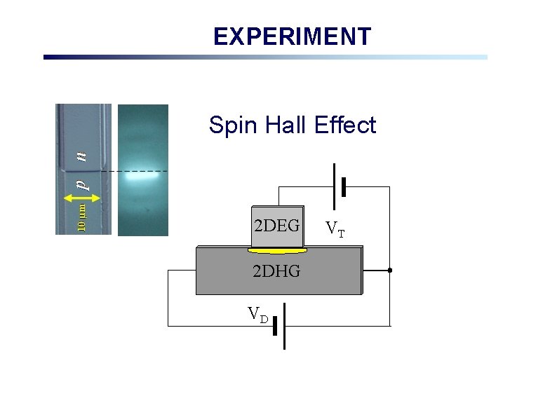
Conventional vertical spin-LED Y. Ohno et al. : Nature 402, 790 (1999) R. Fiederling et al. : Nature 402, 787 (1999) B. T. Jonker et al. : PRB 62, 8180 (2000) X. Jiang et al. : PRL 90, 256603 (2003) R. Wang et al. : APL 86, 052901 (2005) Novel co-planar spin-LED ● No hetero-interface along the LED current ● Spin detection directly in the 2 DHG ● Light emission near edge of the 2 DHG ● 2 DHG with strong and tunable SO … 2 DHG 2 DEG Spin polarization detected through circular polarization of emitted light
EXPERIMENT Spin Hall Effect 2 DEG 2 DHG VD VT
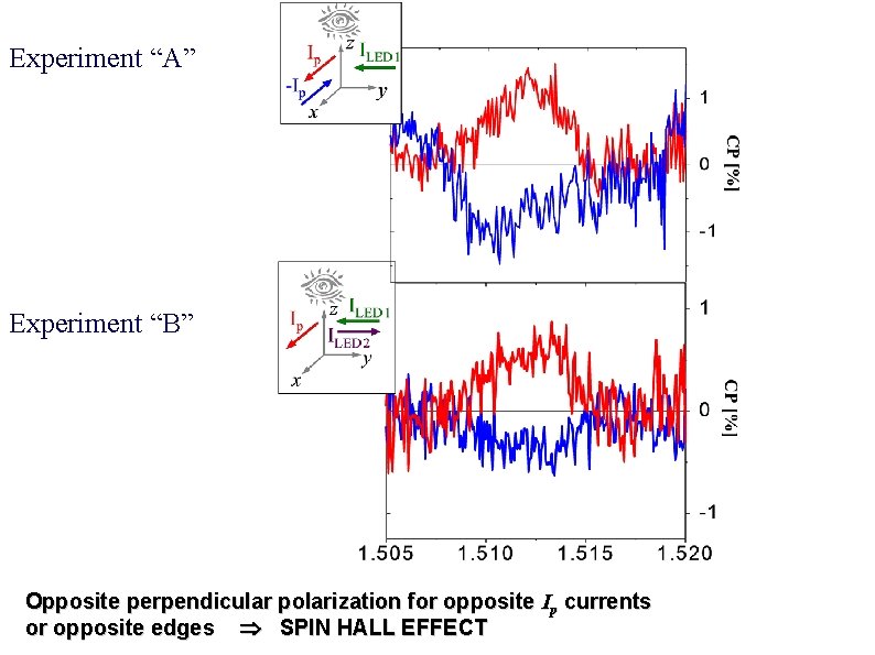
Spin Hall Effect Device Experiment “A” Experiment “B”
Experiment “A” Experiment “B” Opposite perpendicular polarization for opposite Ip currents or opposite edges SPIN HALL EFFECT
FERROMAGNETIC SEMICONDUCTORS
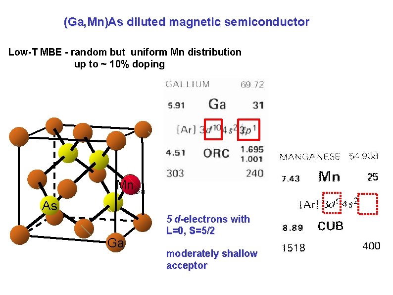
(Ga, Mn)As diluted magnetic semiconductor Low-T MBE - random but uniform Mn distribution up to ~ 10% doping Mn. Ga As Ga 5 d-electrons with L=0, S=5/2 moderately shallow acceptor
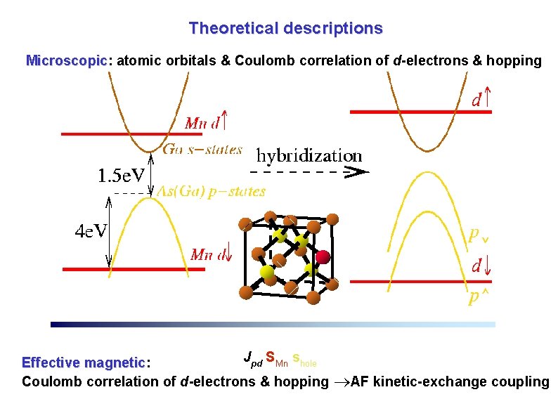
Theoretical descriptions Microscopic: Microscopic atomic orbitals & Coulomb correlation of d-electrons & hopping Jpd = + 0. 6 me. V nm 3 Jpd SMn. shole Effective magnetic: magnetic Coulomb correlation of d-electrons & hopping AF kinetic-exchange coupling
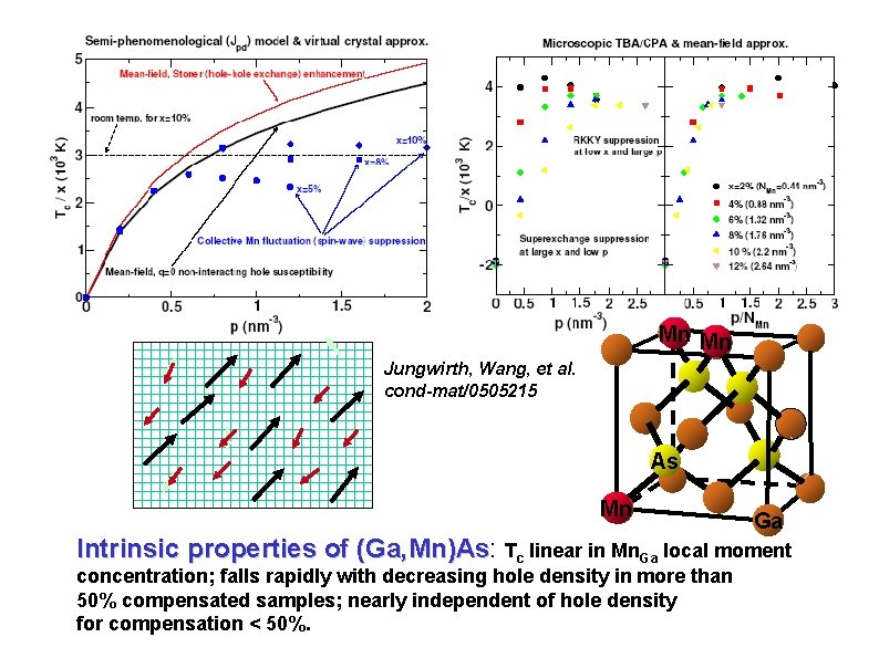
Mn Mn Jungwirth, Wang, et al. cond-mat/0505215 As Mn Ga Intrinsic properties of (Ga, Mn)As: Ga, Mn)As Tc linear in Mn. Ga local moment concentration; falls rapidly with decreasing hole density in more than 50% compensated samples; nearly independent of hole density for compensation < 50%.
Extrinsic effects: Interstitial Mn - a magnetism killer Interstitial Mn is detrimental to magnetic order: compensating double-donor – reduces carrier density couples antiferromagnetically to substitutional Mn even in low compensation samples smaller effective number of Mn moments Blinowski PRB ‘ 03, Mašek, Máca PRB '03 Mn As Yu et al. , PRB ’ 02: ~10 -20% of total Mn concentration is incorporated as interstitials Increased TC on annealing corresponds to removal of these defects.
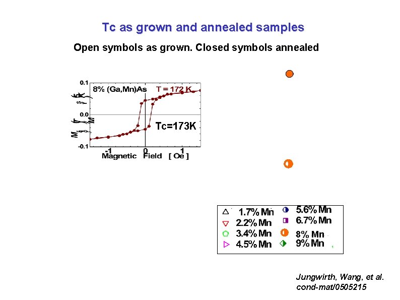
Tc as grown and annealed samples Open symbols as grown. Closed symbols annealed Tc=173 K 8% Mn Jungwirth, Wang, et al. cond-mat/0505215
Tc/xeff vs p/Mneff High (>40%) compensation Jungwirth, Wang, et al. cond-mat/0505215 Number of holes per Mneff
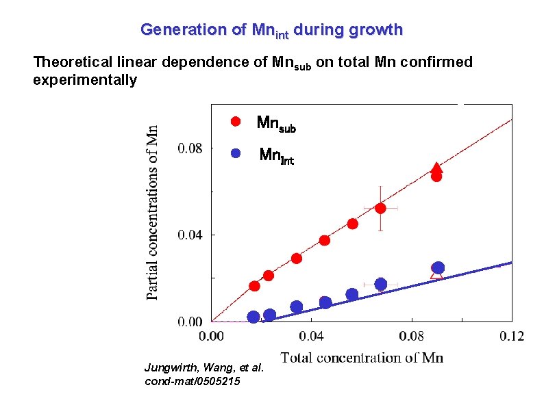
Generation of Mnint during growth Theoretical linear dependence of Mnsub on total Mn confirmed experimentally Mnsub Mn. Int Jungwirth, Wang, et al. cond-mat/0505215
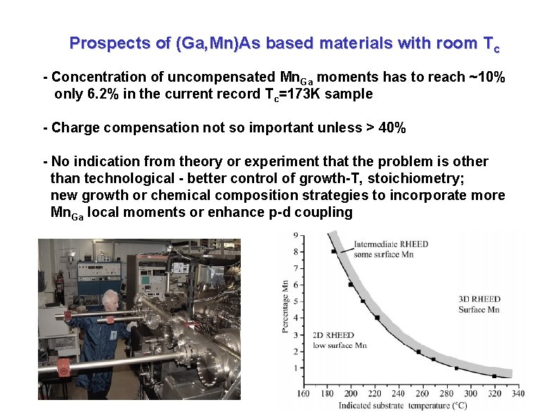
Prospects of (Ga, Mn)As based materials with room Tc - Concentration of uncompensated Mn. Ga moments has to reach ~10% only 6. 2% in the current record Tc=173 K sample - Charge compensation not so important unless > 40% - No indication from theory or experiment that the problem is other than technological - better control of growth-T, stoichiometry; new growth or chemical composition strategies to incorporate more Mn. Ga local moments or enhance p-d coupling
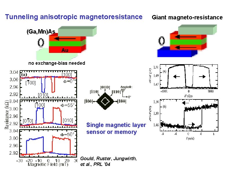
Tunneling anisotropic magnetoresistance (Ga, Mn)As Au Au no exchange-bias needed [100] [010] Single magnetic layer sensor or memory Gould, Ruster, Jungwirth, et al. , PRL '04 Giant magneto-resistance
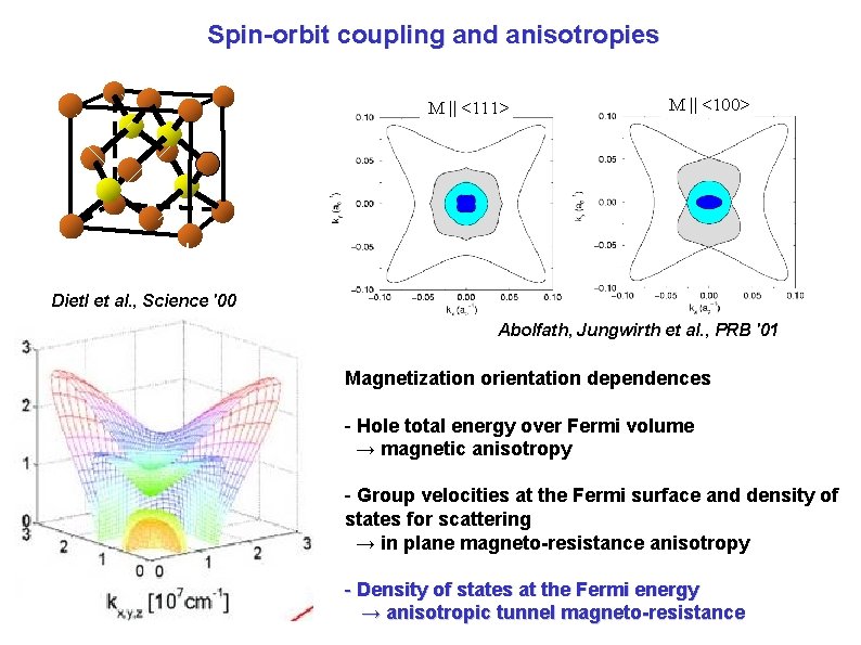
Spin-orbit coupling and anisotropies M || <111> M || <100> spin-split bands at M≠ 0 Dietl et al. , Science '00 (Abolfath, Jungwirth et al. , PRB '01 Magnetization orientation dependences - Hole total energy over Fermi volume → magnetic anisotropy - Group velocities at the Fermi surface and density of states for scattering → in plane magneto-resistance anisotropy - Density of states at the Fermi energy → anisotropic tunnel magneto-resistance
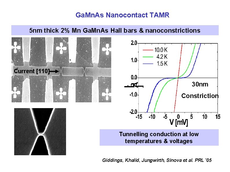
Ga. Mn. As Nanocontact TAMR 5 nm thick 2% Mn Ga. Mn. As Hall bars & nanoconstrictions Current [110] 30 nm Constriction constriction Tunnelling conduction at low temperatures & voltages Giddings, Khalid, Jungwirth, Sinova et al. PRL '05
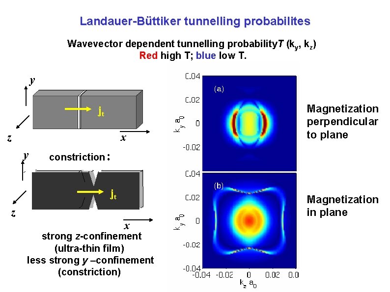
Landauer-Büttiker tunnelling probabilites Wavevector dependent tunnelling probability. T (ky, kz) Red high T; blue low T. y Magnetisation in plane jt z x y Magnetization perpendicular to plane constriction: jt Magnetization in plane z x strong z-confinement (ultra-thin film) less strong y –confinement (constriction)
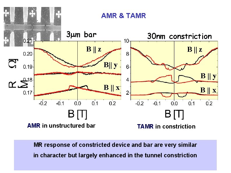
30 nm constriction Very large TAMR in single nanocontacts 1400%
AMR & TAMR 3 m bar 30 nm constriction B || z B|| y B || x AMR in unstructured bar B || x TAMR in constriction MR response of constricted device and bar are very similar in character but largely enhanced in the tunnel constriction
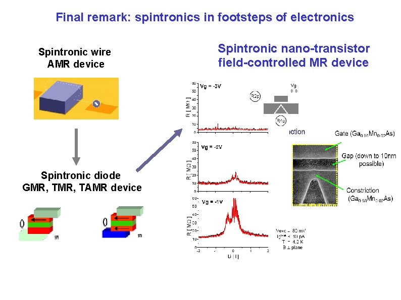
Final remark: spintronics in footsteps of electronics Spintronic wire AMR device Spintronic diode GMR, TAMR device Spintronic nano-transistor field-controlled MR device