CCE 201 Solid State Electronic Devices EEC 223



- Slides: 71

CCE 201: Solid State Electronic Devices EEC 223: Electronics (1) Lecture 04: Diodes Prepared By Dr. Eng. Sherif Hekal Assistant Professor, CCE department Lecture 01 11/30/2020 1

Report 01 – Sol. • Prove that the built-in potential across the PN junction is given by • Solution: when no voltage applied and at equilibrium, no current flows and we have Note: 11/30/2020 2

Introduction • In this Lecture we will learn • the characteristics of the ideal diode and how to analyze and design circuits containing multiple ideal diodes together with resistors and dc sources • the i-v characteristic of the junction diode and how to use it to analyze diode circuits operating in the various bias regions: forward, reverse, and breakdown • a simple but effective model of the diode i-v characteristic in the forward direction: the constantvoltage-drop model 11/30/2020 3

Introduction • a powerful technique for the application and modeling of the diode (and in later chapters, transistors): dc-biasing the diode and modeling its operation for small signals around the dc-operating point by means of the small-signal model • the use of a string of forward-biased diodes and of diodes operating in the breakdown region (zener diodes), to provide constant dc voltages (voltage regulators) • application of the diode in the design of rectifier circuits, which convert ac voltages to dc as needed for powering electronic equipment • a number of other practical and important 11/30/2020 4 applications

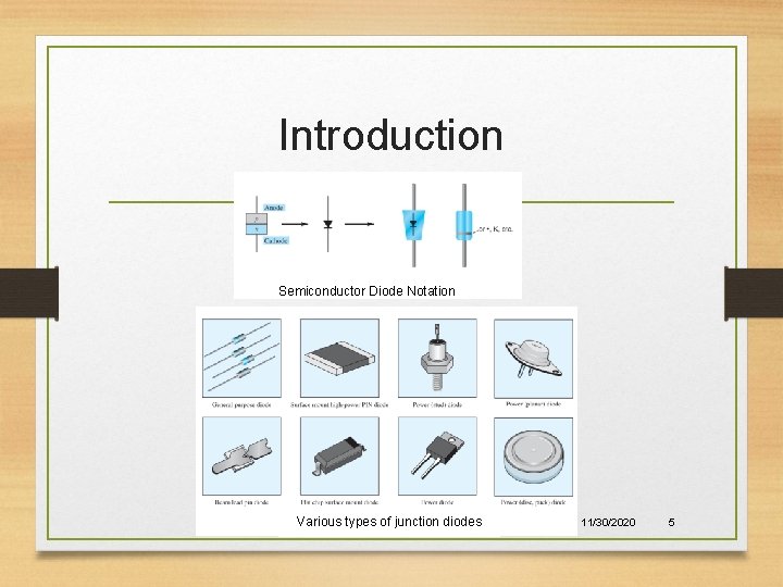
Introduction Semiconductor Diode Notation Various types of junction diodes 11/30/2020 5

Diode Testing • Diode Checking Function • Ohmmeter Testing • Curve Tracer 6

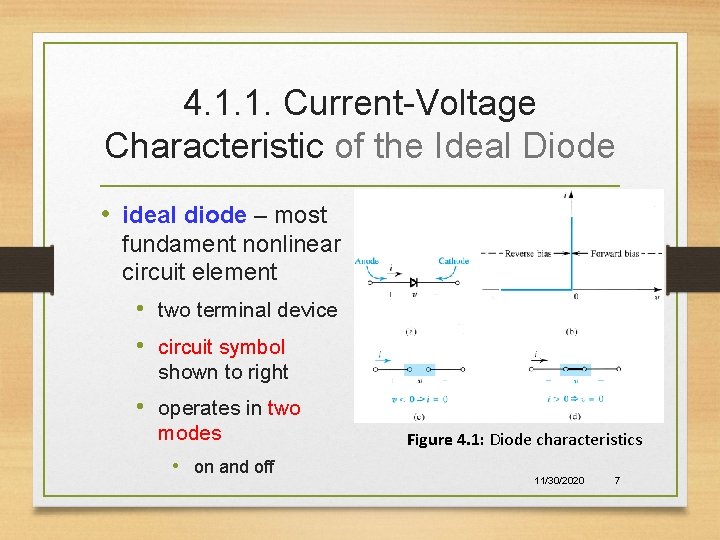
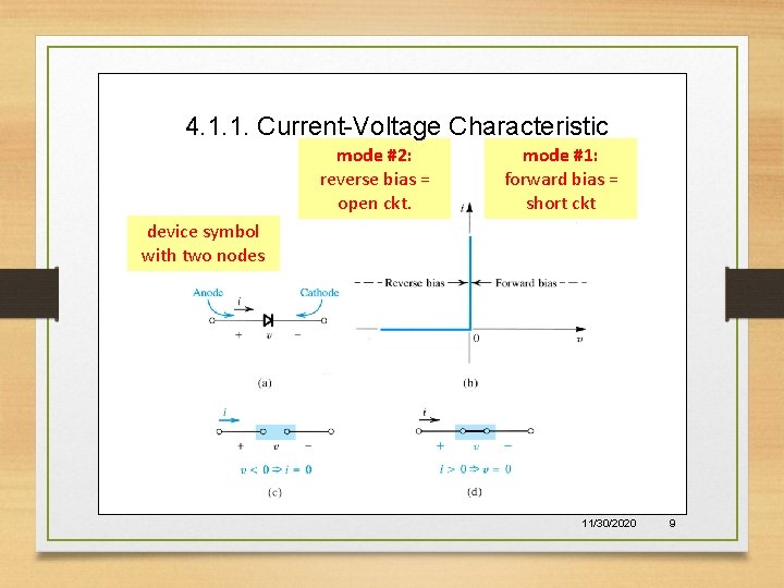
4. 1. 1. Current-Voltage Characteristic of the Ideal Diode • ideal diode – most fundament nonlinear circuit element • two terminal device • circuit symbol shown to right • operates in two modes • on and off Figure 4. 1: Diode characteristics 11/30/2020 7

4. 1. 1. Current-Voltage Characteristic • cathode – negative terminal, from which current flows • anode – positive terminal of diode, into which current flows • voltage-current (VI) behavior is: • nonlinear curve consists of straight-line segments and it is called piecewise linear. 11/30/2020 8

4. 1. 1: Current-Voltage 4. 1. 1. Current-Voltage Characteristic of the Ideal Diode mode #2: mode #1: reverse bias = forward bias = open ckt. short ckt • ideal diode: is most fundament device symbol nonlinear circuit element with two nodes • two terminal device with circuit symbol to right • operates in two modes forward and reverse bias figure 4. 1. 11/30/2020 9

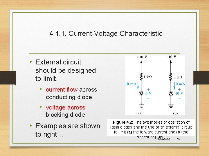
4. 1. 1. Current-Voltage Characteristic • External circuit should be designed to limit… • current flow across conducting diode • voltage across blocking diode • Examples are shown to right… Figure 4. 2: The two modes of operation of ideal diodes and the use of an external circuit to limit (a) the forward current and (b) the reverse voltage. 11/30/2020 10

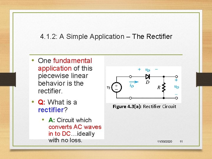
4. 1. 2: A Simple Application – The Rectifier • One fundamental application of this piecewise linear behavior is the rectifier. • Q: What is a rectifier? • A: Circuit which converts AC waves in to DC…ideally with no loss. Figure 4. 3(a): Rectifier Circuit 11/30/2020 11

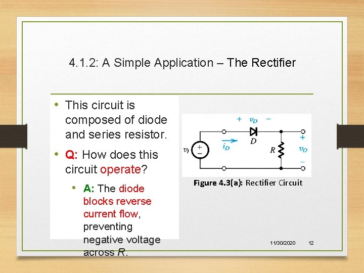
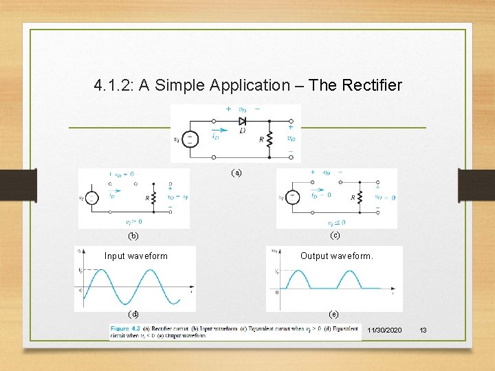
4. 1. 2: A Simple Application – The Rectifier • This circuit is composed of diode and series resistor. • Q: How does this circuit operate? • A: The diode blocks reverse current flow, preventing negative voltage across R. Figure 4. 3(a): Rectifier Circuit 11/30/2020 12

4. 1. 2: A Simple Application – The Rectifier (a) (b) (c) Input waveform Output waveform. (d) (e) 11/30/2020 13

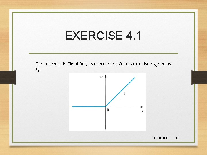
EXERCISE 4. 1 For the circuit in Fig. 4. 3(a), sketch the transfer characteristic v. O versus v. I. 11/30/2020 14

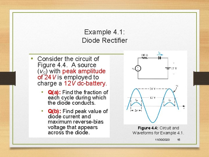
Example 4. 1: Diode Rectifier • Consider the circuit of Figure 4. 4. A source (v. S) with peak amplitude of 24 V is employed to charge a 12 V dc-battery. • Q(a): Find the fraction of each cycle during which the diode conducts. • Q(b): Find peak value of diode current and maximum reverse-bias voltage that appears across the diode. Figure 4. 4: Circuit and Waveforms for Example 4. 1. 11/30/2020 15

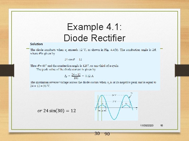
Example 4. 1: Diode Rectifier 11/30/2020 16

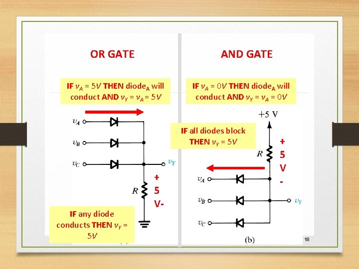
4. 1. 3. Another Application, Diode Logic Gates • Q: How may diodes be used to create logic gates? • A: Examples of AND / OR gates are shown right. • Refer to next Figure 4. 5: Diode logic gates: (a) OR gate; (b) AND gate (in a positive-logic system). slide. 11/30/2020 17

OR GATE AND GATE IF v. A = 5 V THEN diode. A will conduct AND v. Y = v. A = 5 V IF v. A = 0 V THEN diode. A will conduct AND v. Y = v. A = 0 V IF all diodes block THEN v. Y = 5 V IF any diode conducts THEN v. Y = 5 V + 5 V- + 5 V - 11/30/2020 18

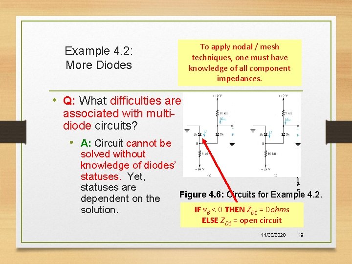
Example 4. 2: More Diodes To apply nodal / mesh techniques, one must have knowledge of all component impedances. • Q: What difficulties are Figure 4. 4: Circuit and Waveforms for Example 4. 1. associated with multidiode circuits? • A: Circuit cannot be solved without knowledge of diodes’ statuses. Yet, statuses are Figure 4. 6: Circuits for Example 4. 2. dependent on the IF v. B < 0 THEN ZD 1 = 0 ohms solution. ELSE ZD 1 = open circuit 11/30/2020 19

Example 4. 2: More Diodes • Q: How does one solve these circuits? • A: One must use the following steps… • 1) assume the status of all diodes • 2) solve via mesh / nodal analysis • 3) check for coherence 11/30/2020 20

Example 4. 2: More Diodes If answer to either of these is no, then the solution is not physically realizable. • Q: How does one check for coherence? • A: One must ask the following questions… • 1) Are calculated voltages across all “assumed conducting” diodes forward-biased? • 2) Are the calculated currents through all “assumed blocking” diodes zero? • Q: What does one do, if the solution is not coherent? • A: One must change one or more of these assumptions and solve as well as check for coherence again. 11/30/2020 21

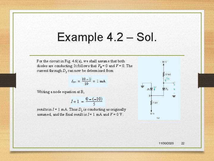
Example 4. 2 – Sol. For the circuit in Fig. 4. 6(a), we shall assume that both diodes are conducting. It follows that VB = 0 and V = 0. The current through D 2 can now be determined from Writing a node equation at B, results in I = 1 m. A. Thus D 1 is conducting as originally assumed, and the final result is I = 1 m. A and V = 0 V. 11/30/2020 22

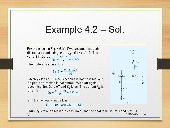
Example 4. 2 – Sol. For the circuit in Fig. 4. 6(b), if we assume that both diodes are conducting, then VB = 0 and V = 0. The current in D 2 is obtained from The node equation at B is which yields I = − 1 m. A. Since this is not possible, our original assumption is not correct. We start again, assuming that D 1 is off and D 2 is on. The current ID 2 is given by and the voltage at node B is Thus D 1 is reverse biased as assumed, and the final result is I = 0 and V = 3. 3 11/30/2020 V. 23

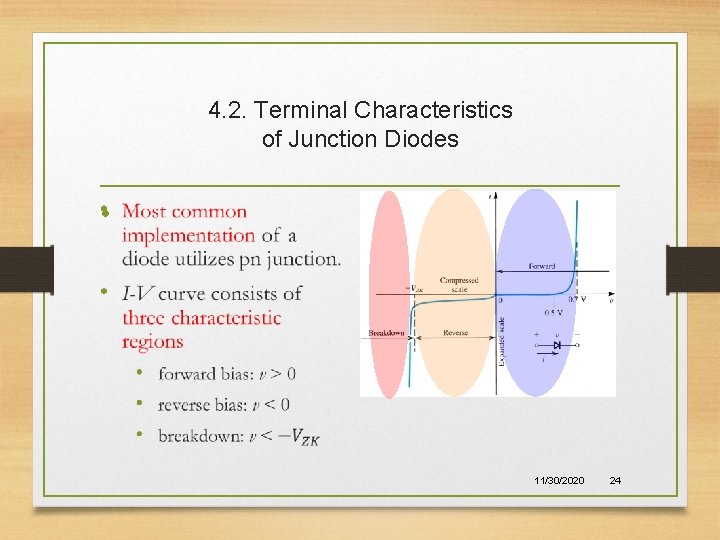
4. 2. Terminal Characteristics of Junction Diodes • 11/30/2020 24

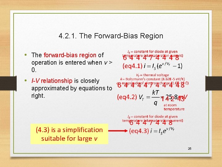
4. 2. 1. The Forward-Bias Region • The forward-bias region of operation is entered when v > 0. • I-V relationship is closely approximated by equations to right. (4. 3) is a simplification suitable for large v 25

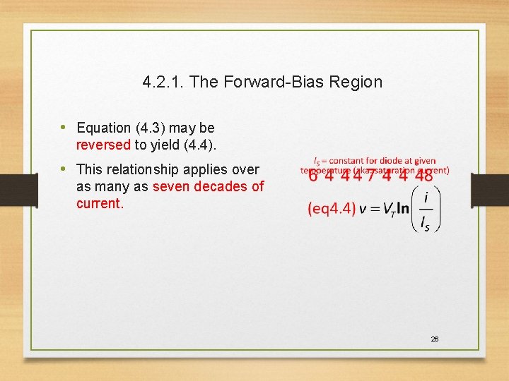
4. 2. 1. The Forward-Bias Region • Equation (4. 3) may be reversed to yield (4. 4). • This relationship applies over as many as seven decades of current. 26

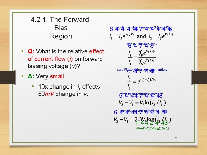
4. 2. 1. The Forward. Bias Region • Q: What is the relative effect of current flow (i) on forward biasing voltage (v)? • A: Very small. • 10 x change in i, effects 60 m. V change in v. 27

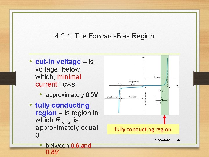
4. 2. 1: The Forward-Bias Region • cut-in voltage – is voltage, below which, minimal current flows • approximately 0. 5 V • fully conducting region – is region in which Rdiode is approximately equal 0 • between 0. 6 and 0. 8 V fully conducting region 11/30/2020 28

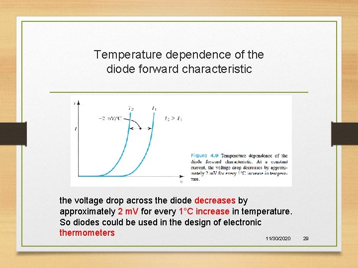
Temperature dependence of the diode forward characteristic the voltage drop across the diode decreases by approximately 2 m. V for every 1°C increase in temperature. So diodes could be used in the design of electronic thermometers 11/30/2020 29

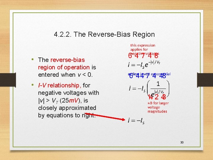
4. 2. 2. The Reverse-Bias Region • The reverse-bias region of operation is entered when v < 0. • I-V relationship, for negative voltages with |v| > VT (25 m. V), is closely approximated by equations to right. 30

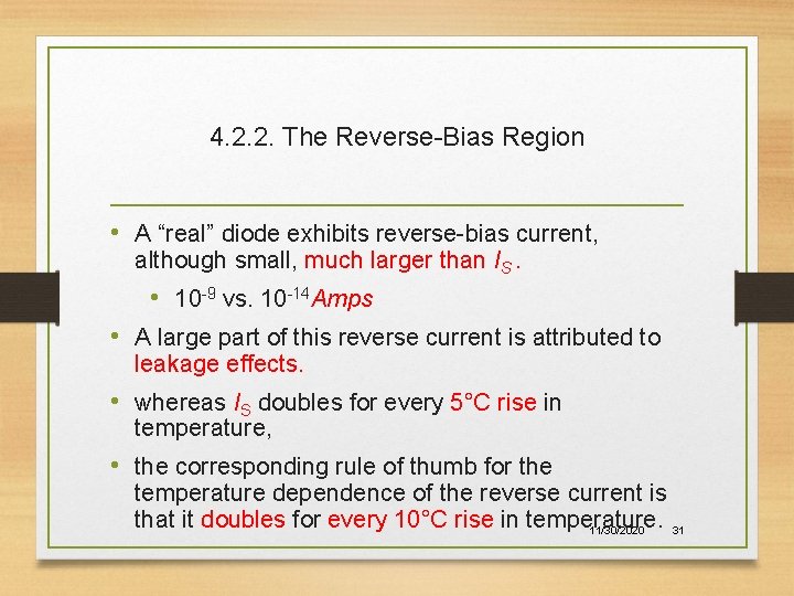
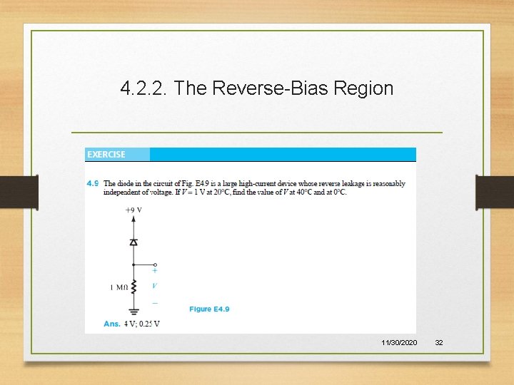
4. 2. 2. The Reverse-Bias Region • A “real” diode exhibits reverse-bias current, although small, much larger than IS. • 10 -9 vs. 10 -14 Amps • A large part of this reverse current is attributed to leakage effects. • whereas IS doubles for every 5°C rise in temperature, • the corresponding rule of thumb for the temperature dependence of the reverse current is that it doubles for every 10°C rise in temperature. 11/30/2020 31

4. 2. 2. The Reverse-Bias Region 11/30/2020 32

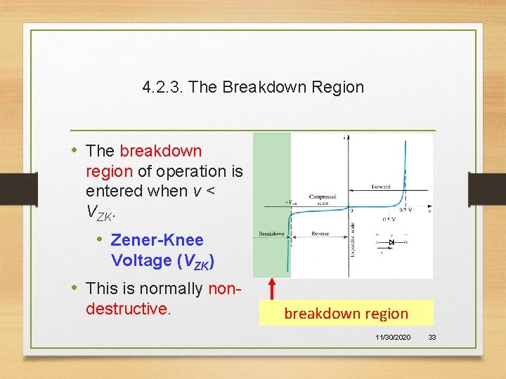
4. 2. 3. The Breakdown Region • The breakdown region of operation is entered when v < VZK. • Zener-Knee Voltage (VZK) • This is normally nondestructive. breakdown region 11/30/2020 33

4. 3. Modeling the Diode Forward Characteristic • We are now ready to consider the analysis of circuits employing forward-conducting diodes. • Upcoming slides, we will discuss simplified diode models better suited for use in circuit analyses: • • exponential model constant voltage-drop model ideal diode model small-signal (linearization) model 11/30/2020 34

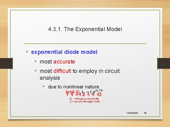
4. 3. 1. The Exponential Model • exponential diode model • most accurate • most difficult to employ in circuit analysis • due to nonlinear nature 11/30/2020 35

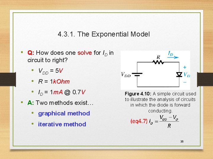
4. 3. 1. The Exponential Model • Q: How does one solve for ID in circuit to right? • VDD = 5 V • R = 1 k. Ohm • ID = 1 m. A @ 0. 7 V • A: Two methods exist… • graphical method • iterative method Figure 4. 10: A simple circuit used to illustrate the analysis of circuits in which the diode is forward conducting. 36

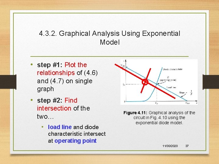
4. 3. 2. Graphical Analysis Using Exponential Model • step #1: Plot the relationships of (4. 6) and (4. 7) on single graph • step #2: Find intersection of the two… • load line and diode Figure 4. 11: Graphical analysis of the circuit in Fig. 4. 10 using the exponential diode model. characteristic intersect at operating point 11/30/2020 37

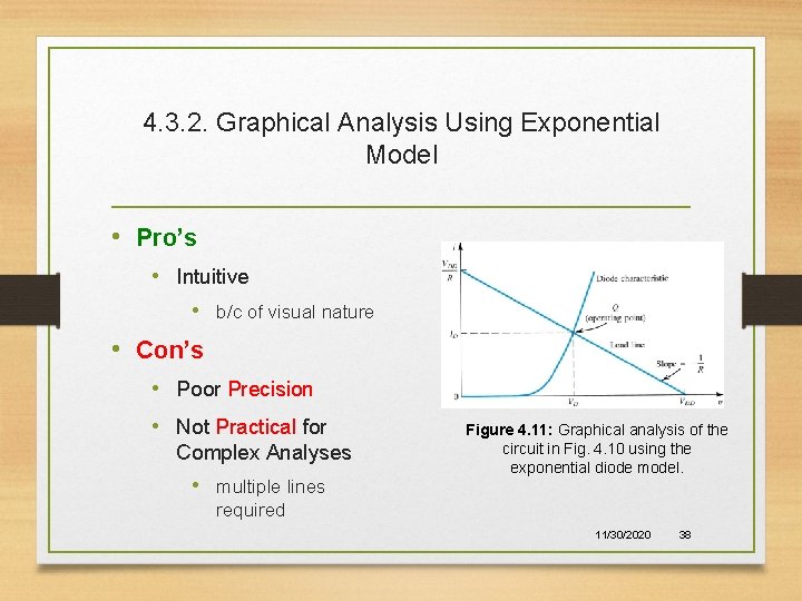
4. 3. 2. Graphical Analysis Using Exponential Model • Pro’s • Intuitive • b/c of visual nature • Con’s • Poor Precision • Not Practical for Complex Analyses • multiple lines Figure 4. 11: Graphical analysis of the circuit in Fig. 4. 10 using the exponential diode model. required 11/30/2020 38

4. 3. 3. Iterative Analysis Using Exponential Method • step #1: Start with initial guess of VD. • VD(0) • step #2: Use nodal / mesh analysis to solve I D. • step #4: Repeat these steps until VD(k+1) = VD(k). • Upon convergence, the new and old values of VD will match. • step #3: Use exponential model to update VD. • VD(1) = f(VD(0)) 11/30/2020 39

4. 3. 3. Iterative Analysis Using Exponential Method • Pro’s • High Precision • Con’s • Not Intuitive • Not Practical for Complex Analyses • 10+ iterations may be required 11/30/2020 40

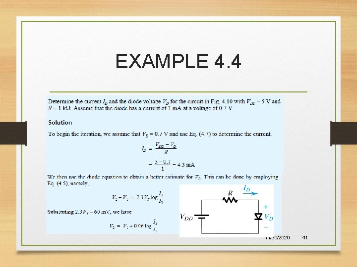
EXAMPLE 4. 4 11/30/2020 41

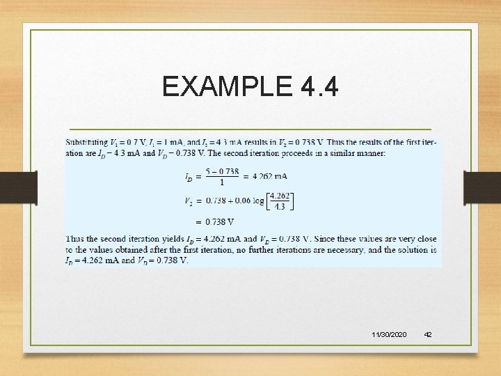
EXAMPLE 4. 4 11/30/2020 42

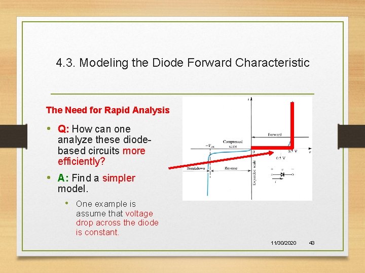
4. 3. Modeling the Diode Forward Characteristic The Need for Rapid Analysis • Q: How can one analyze these diodebased circuits more efficiently? • A: Find a simpler model. • One example is assume that voltage drop across the diode is constant. 11/30/2020 43

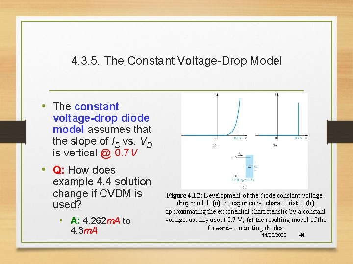
4. 3. 5. The Constant Voltage-Drop Model • The constant voltage-drop diode model assumes that the slope of ID vs. VD is vertical @ 0. 7 V • Q: How does example 4. 4 solution change if CVDM is used? • A: 4. 262 m. A to 4. 3 m. A Figure 4. 12: Development of the diode constant-voltagedrop model: (a) the exponential characteristic; (b) approximating the exponential characteristic by a constant voltage, usually about 0. 7 V; (c) the resulting model of the forward–conducting diodes. 11/30/2020 44

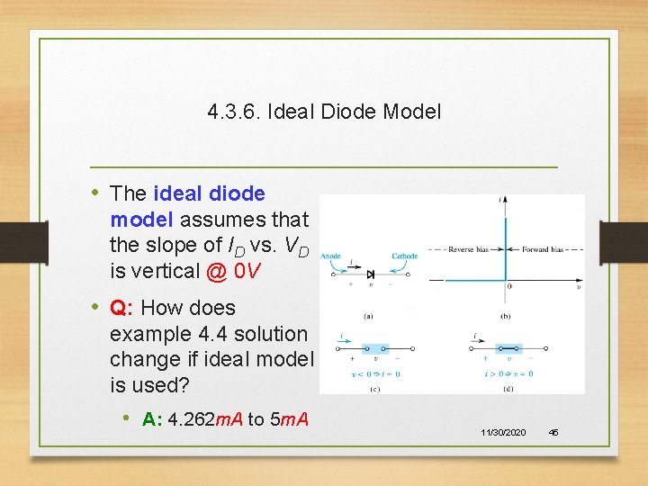
4. 3. 6. Ideal Diode Model • The ideal diode model assumes that the slope of ID vs. VD is vertical @ 0 V • Q: How does example 4. 4 solution change if ideal model is used? • A: 4. 262 m. A to 5 m. A 11/30/2020 45

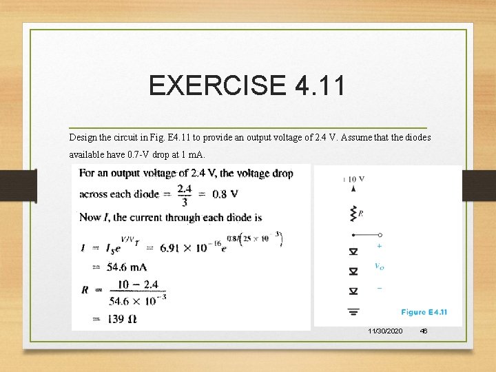
EXERCISE 4. 11 Design the circuit in Fig. E 4. 11 to provide an output voltage of 2. 4 V. Assume that the diodes available have 0. 7 -V drop at 1 m. A. 11/30/2020 46

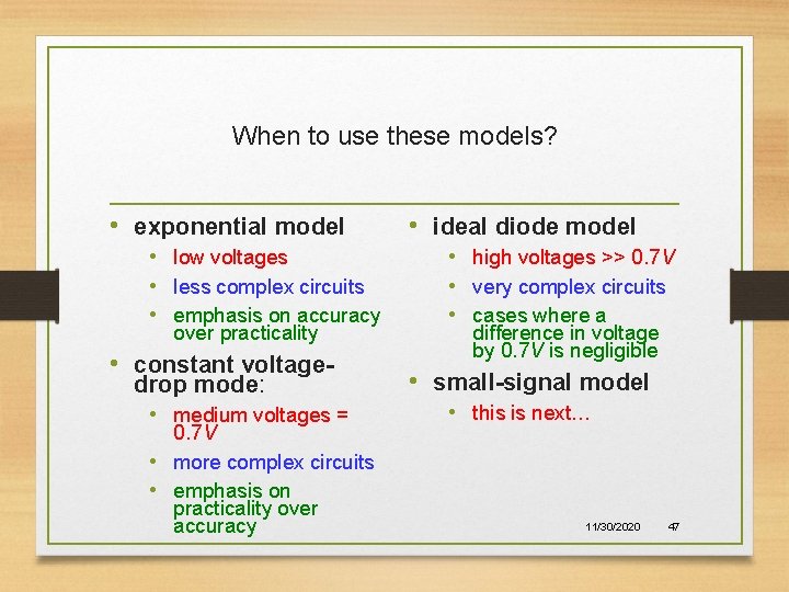
When to use these models? • exponential model • low voltages • less complex circuits • emphasis on accuracy over practicality • constant voltage- drop mode: • medium voltages = 0. 7 V • more complex circuits • emphasis on practicality over accuracy • ideal diode model • high voltages >> 0. 7 V • very complex circuits • cases where a difference in voltage by 0. 7 V is negligible • small-signal model • this is next… 11/30/2020 47

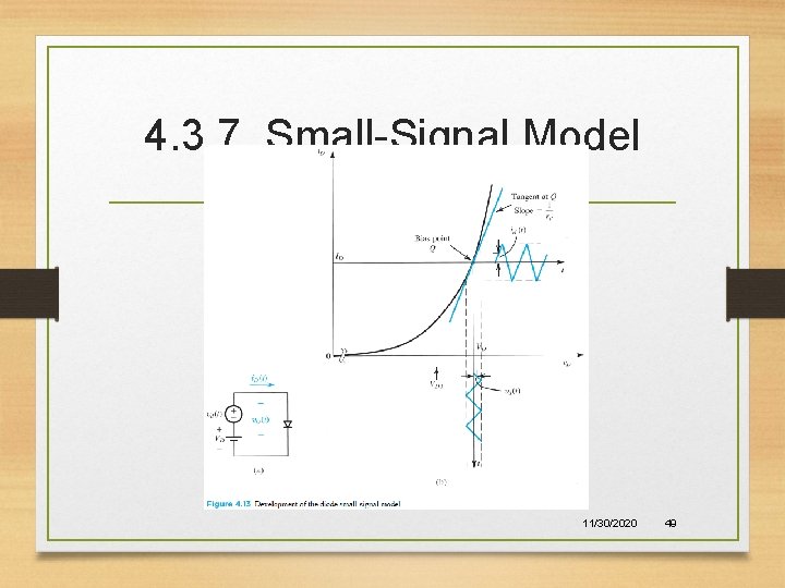
4. 3. 7. Small-Signal Model • small-signal diode model • Diode is modeled as variable resistor. • Whose value is defined via linearization of exponential model. • Around bias point defined by constant voltage drop model. • VD(0) = 0. 7 V 11/30/2020 48

4. 3. 7. Small-Signal Model 11/30/2020 49

4. 3. 7. Small-Signal Model • Q: How is the small-signal diode model defined? • A: The total instantaneous circuit is divided into steady-state and time varying components, which may be analyzed separately and solved via algebra. • In steady-state, diode represented as CVDM. • In time-varying, diode represented as resistor. 11/30/2020 50

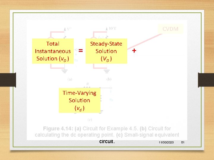
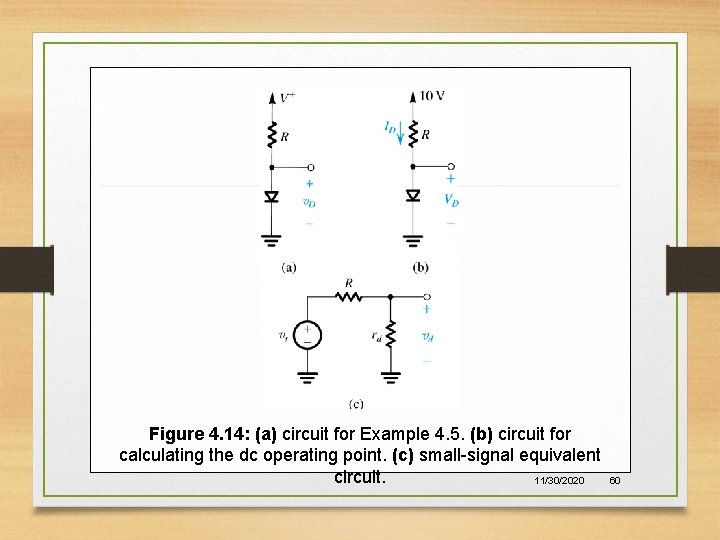
CVDM DC Total Instantaneous AC (v. D. ) Solution = DC Steady-State Solution (VD. ) + Time-Varying AC Solution (vd. ) Figure 4. 14: (a) Circuit for Example 4. 5. (b) Circuit for calculating the dc operating point. (c) Small-signal equivalent circuit. 11/30/2020 51

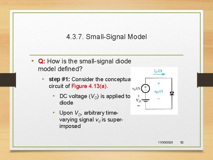
4. 3. 7. Small-Signal Model • Q: How is the small-signal diode model defined? • step #1: Consider the conceptual circuit of Figure 4. 13(a). • DC voltage (VD) is applied to diode • Upon VD, arbitrary time- varying signal vd is superimposed 11/30/2020 52

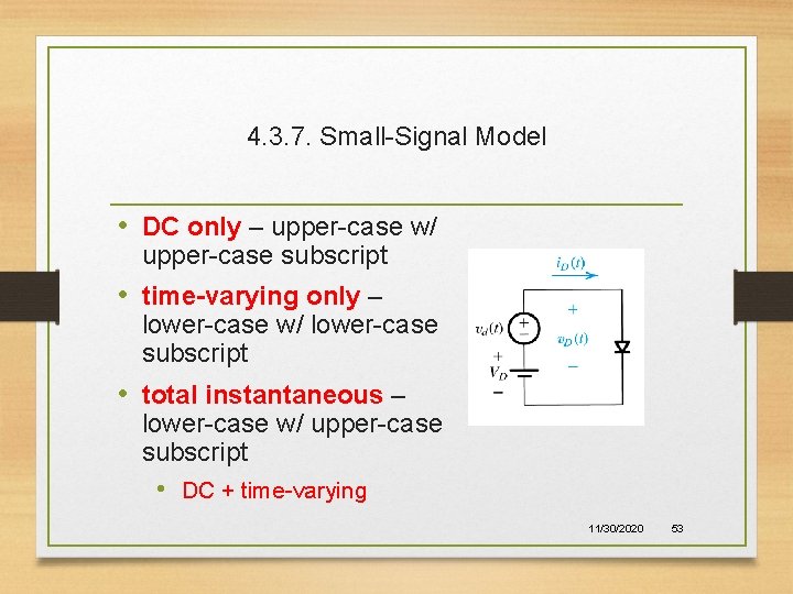
4. 3. 7. Small-Signal Model • DC only – upper-case w/ upper-case subscript • time-varying only – lower-case w/ lower-case subscript • total instantaneous – lower-case w/ upper-case subscript • DC + time-varying 11/30/2020 53

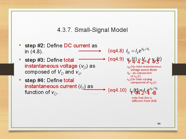
4. 3. 7. Small-Signal Model • step #2: Define DC current as in (4. 8). • step #3: Define total instantaneous voltage (v. D) as composed of VD and vd. • step #4: Define total instantaneous current (i. D) as function of v. D. 54

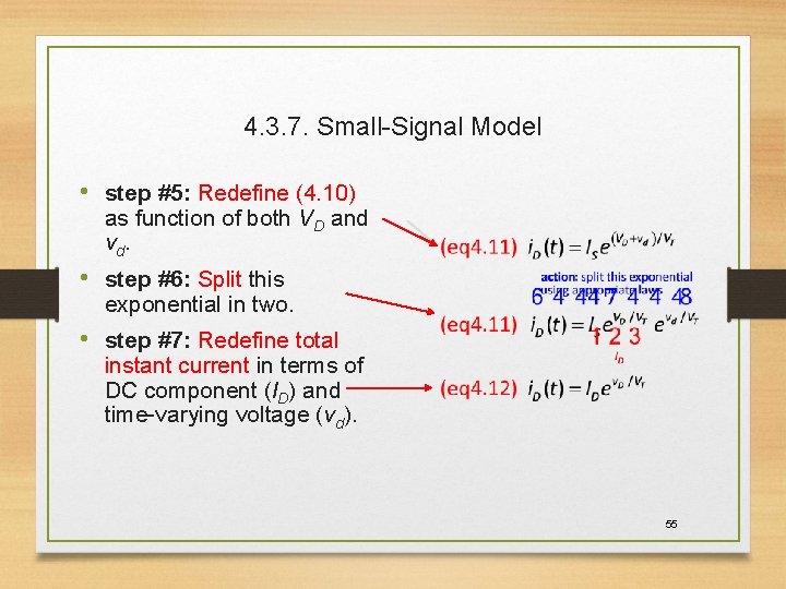
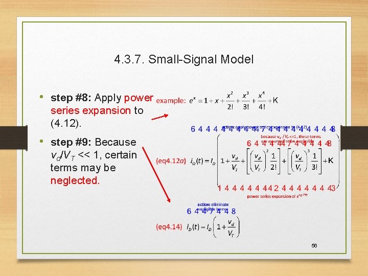
4. 3. 7. Small-Signal Model • step #5: Redefine (4. 10) as function of both VD and vd. • step #6: Split this exponential in two. • step #7: Redefine total instant current in terms of DC component (ID) and time-varying voltage (vd). 55

4. 3. 7. Small-Signal Model • step #8: Apply power series expansion to (4. 12). • step #9: Because vd/VT << 1, certain terms may be neglected. 56

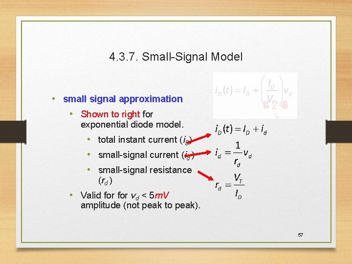
4. 3. 7. Small-Signal Model • small signal approximation • Shown to right for exponential diode model. • total instant current (i. D) • small-signal current (id. ) • small-signal resistance (rd. ) • Valid for vd < 5 m. V amplitude (not peak to peak). 57

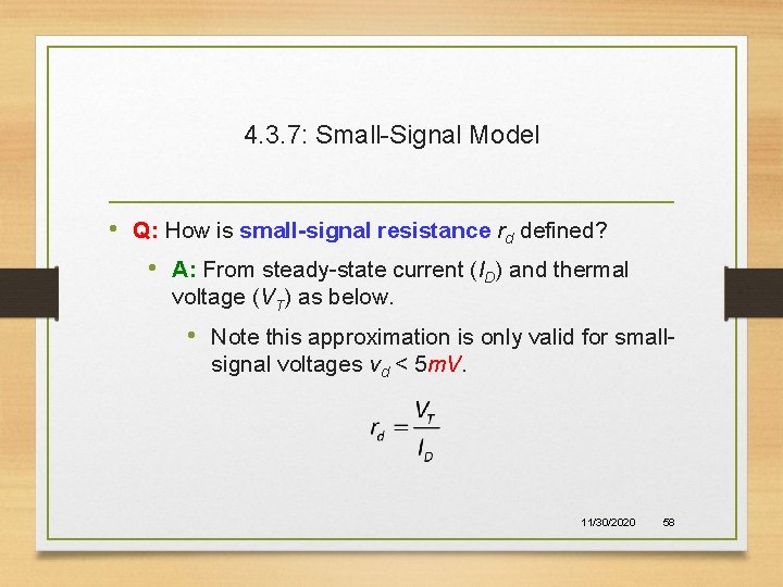
4. 3. 7: Small-Signal Model • Q: How is small-signal resistance rd defined? • A: From steady-state current (ID) and thermal voltage (VT) as below. • Note this approximation is only valid for smallsignal voltages vd < 5 m. V. 11/30/2020 58

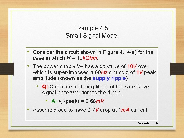
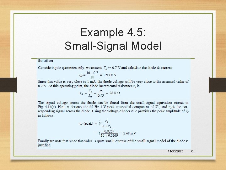
Example 4. 5: Small-Signal Model • Consider the circuit shown in Figure 4. 14(a) for the case in which R = 10 k. Ohm. • The power supply V+ has a dc value of 10 V over which is super-imposed a 60 Hz sinusoid of 1 V peak amplitude (known as the supply ripple) • Q: Calculate both amplitude of the sine-wave signal observed across the diode. • A: vd. (peak) = 2. 68 m. V • Assume diode to have 0. 7 V drop at 1 m. A current. 11/30/2020 59

Figure 4. 14: (a) circuit for Example 4. 5. (b) circuit for calculating the dc operating point. (c) small-signal equivalent circuit. 11/30/2020 60

Example 4. 5: Small-Signal Model 11/30/2020 61

4. 3. 8. Use of Diode Forward Drop in Voltage Regulation • Q: What is a voltage • Q: What regulator? • A: Circuit whose voltage output remains stable in spite of changes in supply and load. characteristic of the diode facilitates voltage regulation? • A: The approximately constant voltage drop across it (0. 7 V). 11/30/2020 62

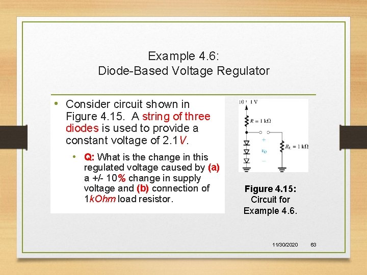
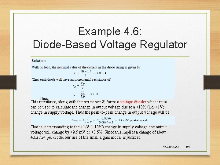
Example 4. 6: Diode-Based Voltage Regulator • Consider circuit shown in Figure 4. 15. A string of three diodes is used to provide a constant voltage of 2. 1 V. • Q: What is the change in this regulated voltage caused by (a) a +/- 10% change in supply voltage and (b) connection of 1 k. Ohm load resistor. Figure 4. 15: Circuit for Example 4. 6. 11/30/2020 63

Example 4. 6: Diode-Based Voltage Regulator Thus, This resistance, along with the resistance R, forms a voltage divider whose ratio can be used to calculate the change in output voltage due to a ± 10% (i. e. ± 1 V) change in supply voltage. Thus the peak-to-peak change in output voltage will be That is, corresponding to the ± 1 -V (± 10%) change in supply voltage, the output voltage will change by ± 9. 5 m. V or ± 0. 5%. Since this implies a change of about ± 3. 2 m. V per diode, our use of the small signal model is justified. 11/30/2020 64

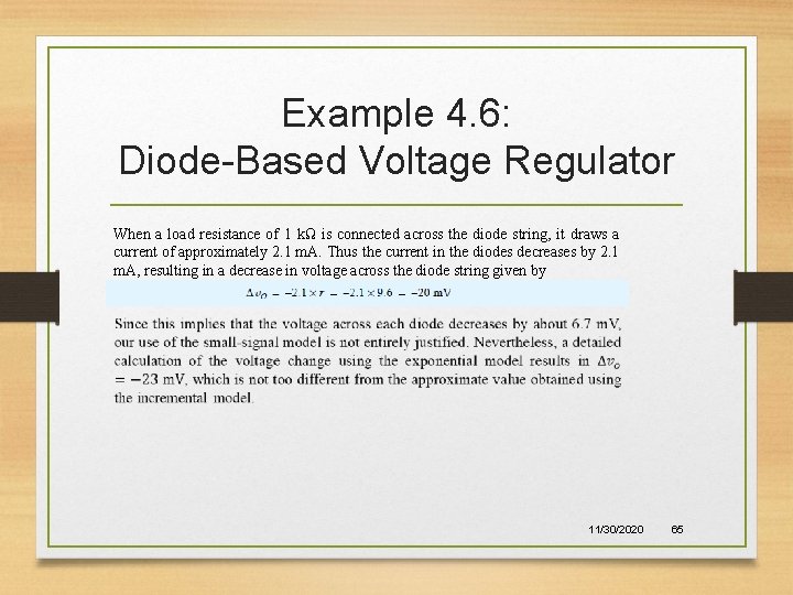
Example 4. 6: Diode-Based Voltage Regulator When a load resistance of 1 kΩ is connected across the diode string, it draws a current of approximately 2. 1 m. A. Thus the current in the diodes decreases by 2. 1 m. A, resulting in a decrease in voltage across the diode string given by 11/30/2020 65

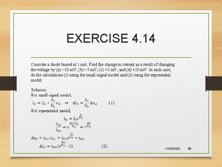
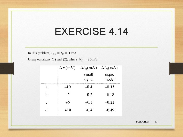
EXERCISE 4. 14 Consider a diode biased at 1 m. A. Find the change in current as a result of changing the voltage by (a) − 10 m. V, (b) − 5 m. V, (c) +5 m. V, and (d) +10 m. V. In each case, do the calculations (i) using the small-signal model and (ii) using the exponential model. 11/30/2020 66

EXERCISE 4. 14 11/30/2020 67

Summary (1) • In the forward direction, the ideal diode conducts any current forced by the external circuit while displaying a zero-voltage drop. The ideal diode does not conduct in reverse direction; any applied voltage appears as reverse bias across the diode. • The unidirectional current flow property makes the diode useful in the design of rectifier circuits. • The forward conduction of practical silicon-junction diodes is accurately characterized by the relationship i = ISe. V/VT. 11/30/2020 71

Summary (2) • A silicon diode conducts a negligible current until the forward voltage is at least 0. 5 V. Then, the current increases rapidly with the voltage drop increasing by 60 m. V for every decade of current change. • In the reverse direction, a silicon diode conducts a current on the order of 10 -9 A. This current is much greater than IS and increases with the magnitude of reverse voltage. 11/30/2020 72

Summary (3) • Beyond a certain value of reverse voltage (that depends on the diode itself), breakdown occurs and current increases rapidly with a small corresponding increase in voltage. • Diodes designed to operate in the breakdown region are called zener diodes. They are employed in the design of voltage regulators whose function is to provide a constant dc voltage that varies little with variations in power supply voltage and / or load current. 11/30/2020 73

Summary (4) • In many applications, a conducting diode is modeled as having a constant voltage drop – usually with value of approximately 0. 7 V. • A diode biased to operate at a dc current ID has small signal resistance rd = VT/ID. • Rectifiers covert ac voltage into unipolar voltages. Half-wave rectifiers do this by passing the voltage in half of each cycle and blocking the oppositepolarity voltage in the other half of the cycle. 11/30/2020 74