CCE 201 Solid State Electronic Devices EEC 223
- Slides: 47

CCE 201: Solid State Electronic Devices EEC 223: Electronics (1) Lecture 08 Field Effect Transistors (1) Prepared By Dr. Eng. Sherif Hekal Assistant Professor, CCE department Lecture 01 11/2/2020 1

Introduction IN THIS LECTURE WE WILL LEARN • General overview on FET transistor and its types. • The physical structure of the MOS transistor and how it works. • How the voltage between two terminals of the transistor control the current that flows through the third terminal, and the equations that describe these current-voltage characteristics. • How the transistor can be used to make an amplifier, and 11/2/2020 how it can be used as a switch in digital circuits. 2

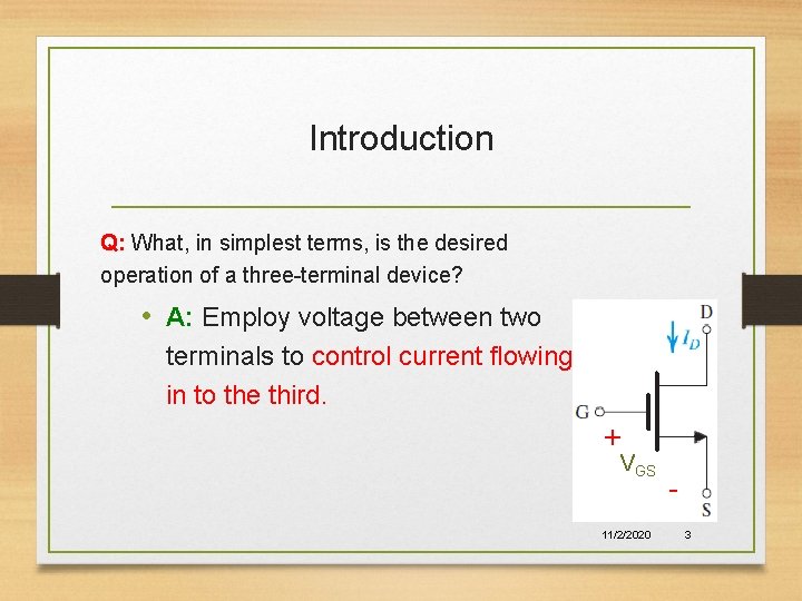
Introduction Q: What, in simplest terms, is the desired operation of a three-terminal device? • A: Employ voltage between two terminals to control current flowing in to the third. + VGS 11/2/2020 3

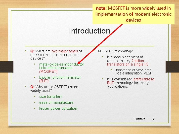
note: MOSFET is more widely used in implementation of modern electronic devices Introduction • Q: What are two major types of three-terminal semiconductor devices? • metal-oxide-semiconductor field-effect transistor (MOSFET) • bipolar junction transistor (BJT) • Q: Why are MOSFET’s more widely used? • MOSFET technology • It allows placement of approximately 2 billion transistors on a single IC • backbone of very large scale integration (VLSI) • It is considered preferable to BJT technology for many applications. • size (smaller) • ease of manufacture • lesser power utilization 11/2/2020 4

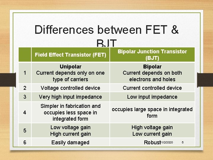
Differences between FET & BJT Bipolar Junction Transistor Field Effect Transistor (FET) (BJT) 1 Unipolar Current depends only on one type of carriers Bipolar Current depends on both electrons and holes 2 Voltage controlled device Current controlled device 3 Very high input impedance Low input impedance 4 Simpler in fabrication and occupies less space in integrated form occupies large space in integrated form 5 Low voltage gain High current gain High voltage gain Low current gain 6 Easily damaged Robust 11/2/2020 5

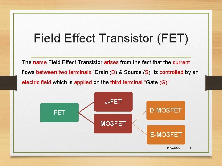
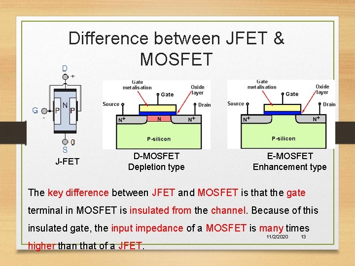
Field Effect Transistor (FET) The name Field Effect Transistor arises from the fact that the current flows between two terminals “Drain (D) & Source (S)” is controlled by an electric field which is applied on the third terminal “Gate (G)” J-FET D-MOSFET E-MOSFET 11/2/2020 6

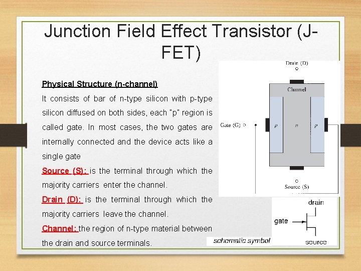
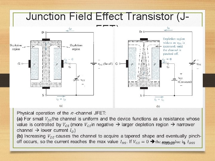
Junction Field Effect Transistor (JFET) Physical Structure (n-channel) It consists of bar of n-type silicon with p-type silicon diffused on both sides, each “p” region is called gate. In most cases, the two gates are internally connected and the device acts like a single gate Source (S): is the terminal through which the majority carriers enter the channel. Drain (D): is the terminal through which the majority carriers leave the channel. Channel: the region of n-type material between the drain and source terminals. 11/2/2020 7

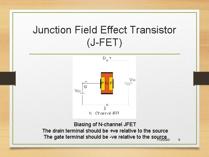
Junction Field Effect Transistor (J-FET) Biasing of N-channel JFET The drain terminal should be +ve relative to the source The gate terminal should be -ve relative to the source 11/2/2020 8

Junction Field Effect Transistor (JFET) 11/2/2020 9

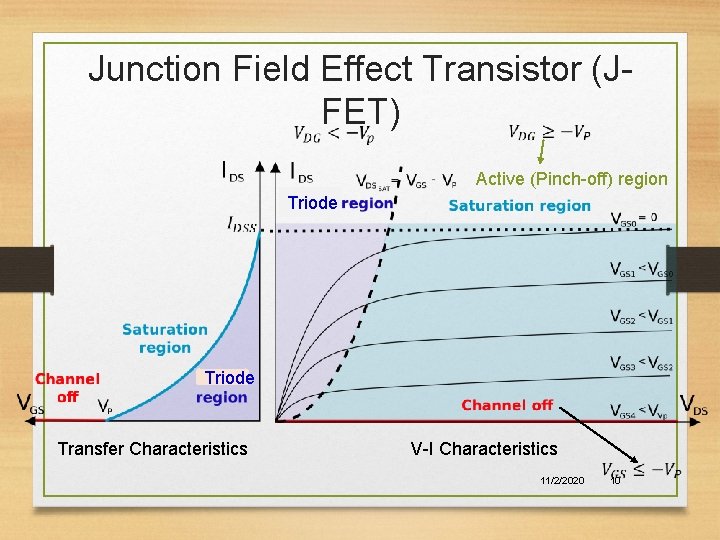
Junction Field Effect Transistor (JFET) Active (Pinch-off) region Triode Transfer Characteristics V-I Characteristics 11/2/2020 10

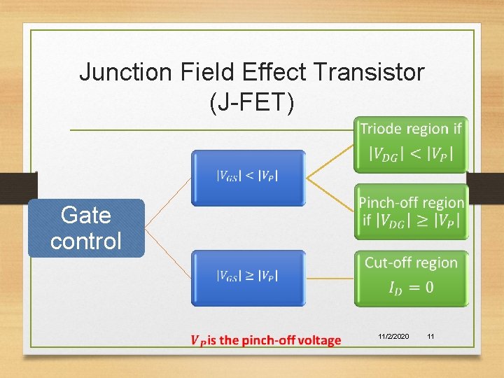
Junction Field Effect Transistor (J-FET) Gate control 11/2/2020 11

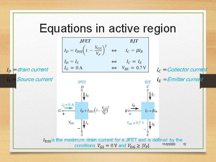
Equations in active region 11/2/2020 12

Difference between JFET & MOSFET J-FET D-MOSFET Depletion type E-MOSFET Enhancement type The key difference between JFET and MOSFET is that the gate terminal in MOSFET is insulated from the channel. Because of this insulated gate, the input impedance of a MOSFET is many times 11/2/2020 higher than that of a JFET. 13

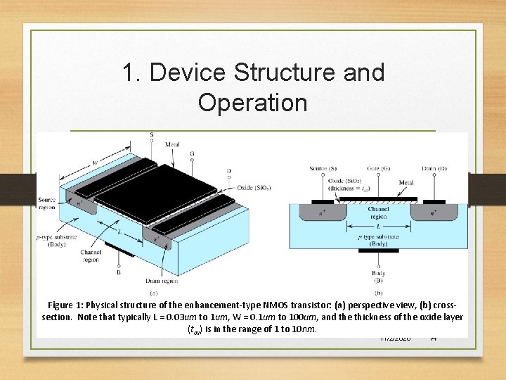
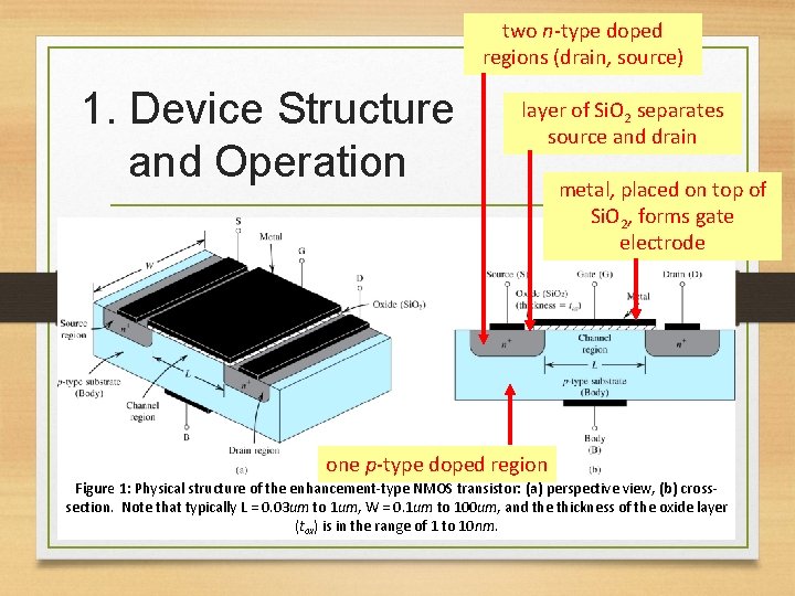
1. Device Structure and Operation Figure 1: Physical structure of the enhancement-type NMOS transistor: (a) perspective view, (b) crosssection. Note that typically L = 0. 03 um to 1 um, W = 0. 1 um to 100 um, and the thickness of the oxide layer (tox) is in the range of 1 to 10 nm. 11/2/2020 14

two n-type doped regions (drain, source) 1. Device Structure and Operation layer of Si. O 2 separates source and drain metal, placed on top of Si. O 2, forms gate electrode one p-type doped region Figure 1: Physical structure of the enhancement-type NMOS transistor: (a) perspective view, (b) crosssection. Note that typically L = 0. 03 um to 1 um, W = 0. 1 um to 100 um, and the thickness of the oxide layer (tox) is in the range of 1 to 10 nm. 11/2/2020 15

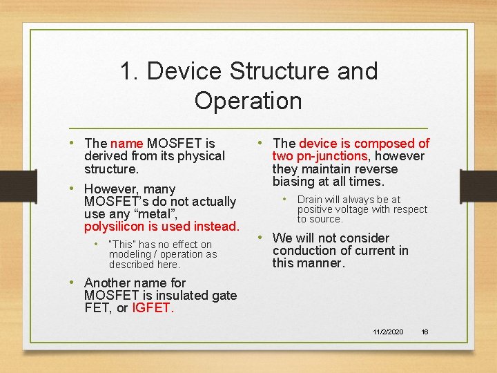
1. Device Structure and Operation • The name MOSFET is derived from its physical structure. • However, many MOSFET’s do not actually use any “metal”, polysilicon is used instead. • “This” has no effect on modeling / operation as described here. • The device is composed of two pn-junctions, however they maintain reverse biasing at all times. • Drain will always be at positive voltage with respect to source. • We will not consider conduction of current in this manner. • Another name for MOSFET is insulated gate FET, or IGFET. 11/2/2020 16

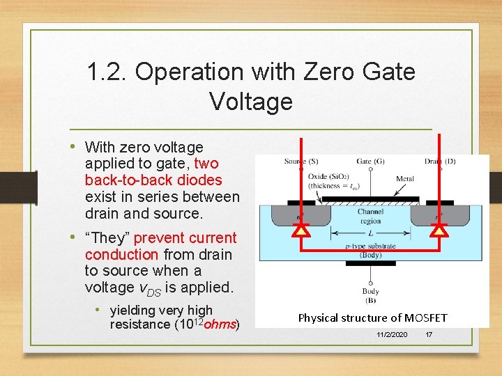
1. 2. Operation with Zero Gate Voltage • With zero voltage applied to gate, two back-to-back diodes exist in series between drain and source. • “They” prevent current conduction from drain to source when a voltage v. DS is applied. • yielding very high resistance (1012 ohms) Physical structure of MOSFET 11/2/2020 17

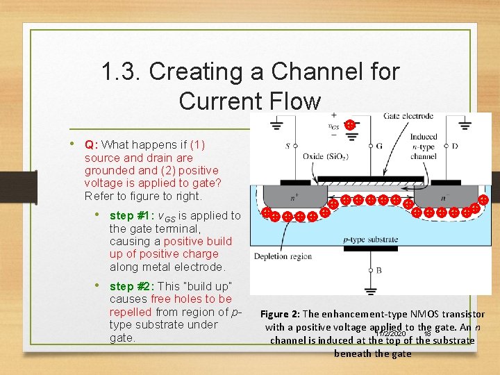
1. 3. Creating a Channel for Current Flow • Q: What happens if (1) source and drain are grounded and (2) positive voltage is applied to gate? Refer to figure to right. • step #1: v. GS is applied to the gate terminal, causing a positive build up of positive charge along metal electrode. • step #2: This “build up” causes free holes to be repelled from region of ptype substrate under gate. Figure 2: The enhancement-type NMOS transistor with a positive voltage applied to the gate. An n 11/2/2020 18 channel is induced at the top of the substrate beneath the gate

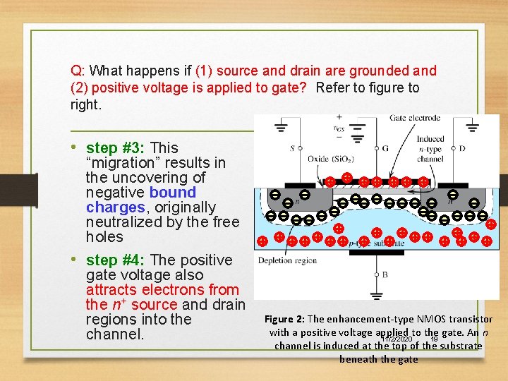
Q: What happens if (1) source and drain are grounded and (2) positive voltage is applied to gate? Refer to figure to right. • step #3: This “migration” results in the uncovering of negative bound charges, originally neutralized by the free holes • step #4: The positive gate voltage also attracts electrons from the n+ source and drain regions into the channel. Figure 2: The enhancement-type NMOS transistor with a positive voltage applied to the gate. An n 11/2/2020 19 channel is induced at the top of the substrate beneath the gate

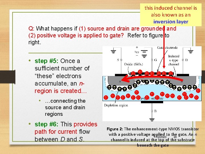
this induced channel is also known as an inversion layer Q: What happens if (1) source and drain are grounded and (2) positive voltage is applied to gate? Refer to figure to right. • step #5: Once a sufficient number of “these” electrons accumulate, an nregion is created… • …connecting the source and drain regions • step #6: This provides path for current flow between D and S. Figure 2: The enhancement-type NMOS transistor with a positive voltage applied to the gate. An n 11/2/2020 20 channel is induced at the top of the substrate beneath the gate

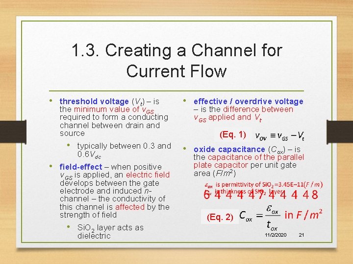
1. 3. Creating a Channel for Current Flow • threshold voltage (Vt) – is the minimum value of v. GS required to form a conducting channel between drain and source • effective / overdrive voltage – is the difference between v. GS applied and Vt. (Eq. 1) • typically between 0. 3 and • oxide capacitance (C ) – is ox 0. 6 Vdc • field-effect – when positive v. GS is applied, an electric field develops between the gate electrode and induced nchannel – the conductivity of this channel is affected by the strength of field • Si. O 2 layer acts as dielectric the capacitance of the parallel plate capacitor per unit gate area (F/m 2) (Eq. 2) 11/2/2020 21

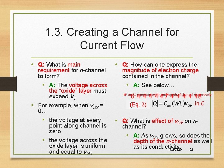
1. 3. Creating a Channel for Current Flow • Q: What is main requirement for n-channel to form? • A: The voltage across the “oxide” layer must exceed Vt. • For example, when v. DS = • Q: How can one express the magnitude of electron charge contained in the channel? • A: See below… (Eq. 3) 0… • the voltage at every point along channel is zero • the voltage across the oxide layer is uniform and equal to v. GS • Q: What is effect of v. OV on nchannel? • A: As v. OV grows, so does the depth of the n-channel as well as its conductivity. 11/2/2020 22

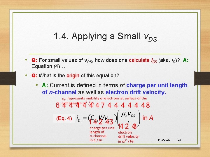
1. 4. Applying a Small v. DS • Q: For small values of v. DS, how does one calculate i. DS (aka. i. D)? A: Equation (4)… • Q: What is the origin of this equation? • A: Current is defined in terms of charge per unit length of n-channel as well as electron drift velocity. (Eq. 4) 11/2/2020 23

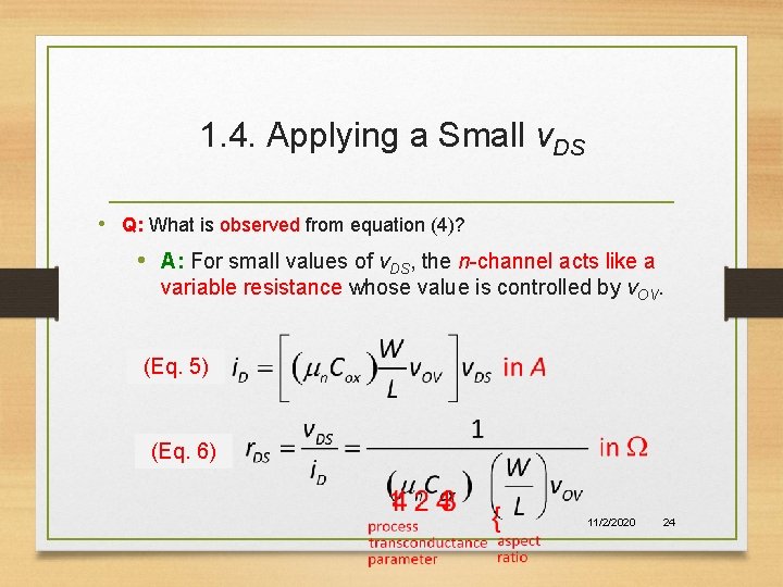
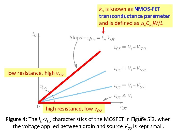
1. 4. Applying a Small v. DS • Q: What is observed from equation (4)? • A: For small values of v. DS, the n-channel acts like a variable resistance whose value is controlled by v. OV. (Eq. 5) (Eq. 6) 11/2/2020 24

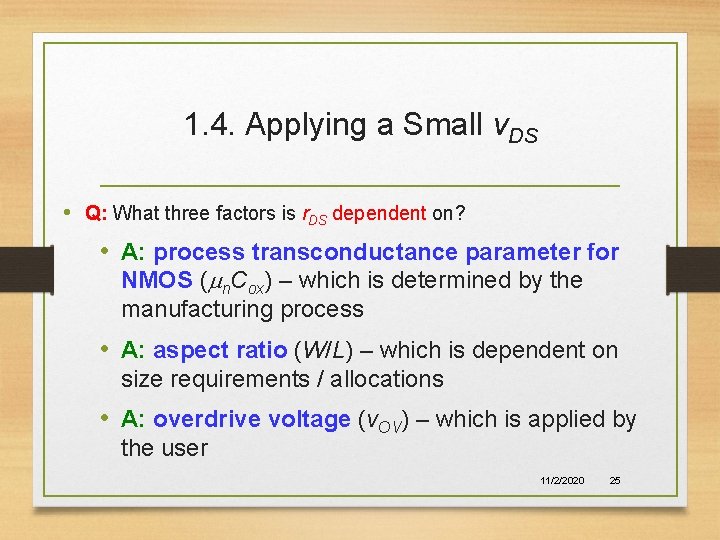
1. 4. Applying a Small v. DS • Q: What three factors is r. DS dependent on? • A: process transconductance parameter for NMOS (mn. Cox) – which is determined by the manufacturing process • A: aspect ratio (W/L) – which is dependent on size requirements / allocations • A: overdrive voltage (v. OV) – which is applied by the user 11/2/2020 25

kn is known as NMOS-FET transconductance parameter and is defined as mn. Cox. W/L 1/r. DS low resistance, high v. OV high resistance, low v. OV 11/2/2020 26 Figure 4: The i. D-v. DS characteristics of the MOSFET in Figure 5. 3. when the voltage applied between drain and source VDS is kept small.

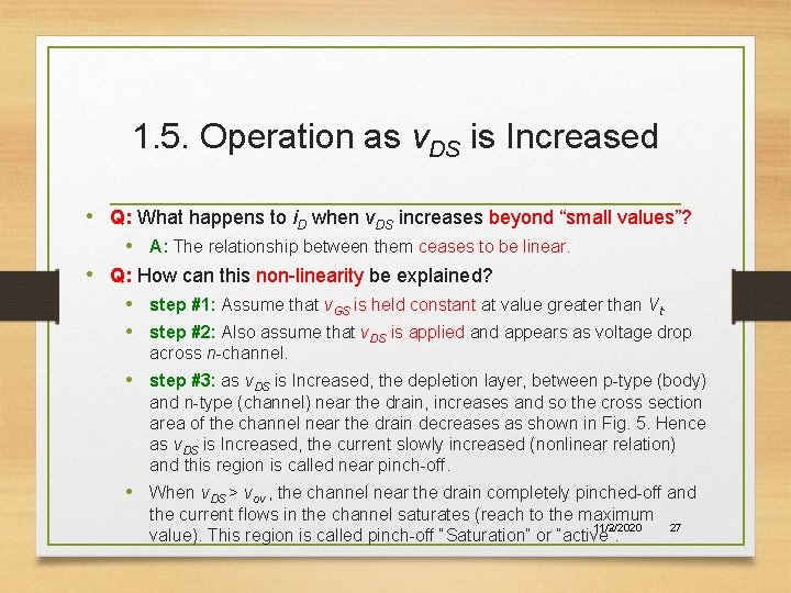
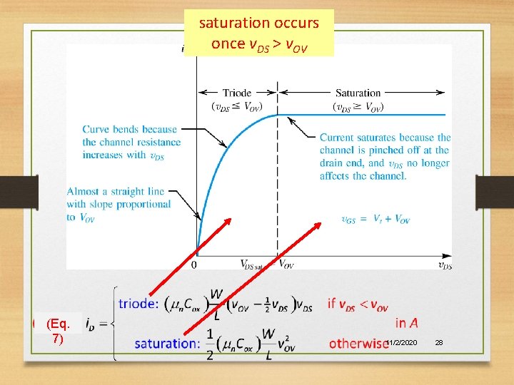
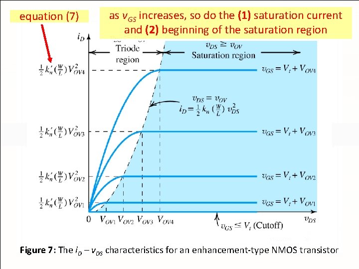
1. 5. Operation as v. DS is Increased • Q: What happens to i. D when v. DS increases beyond “small values”? • A: The relationship between them ceases to be linear. • Q: How can this non-linearity be explained? • step #1: Assume that v. GS is held constant at value greater than Vt. • step #2: Also assume that v. DS is applied and appears as voltage drop across n-channel. • step #3: as v. DS is Increased, the depletion layer, between p-type (body) and n-type (channel) near the drain, increases and so the cross section area of the channel near the drain decreases as shown in Fig. 5. Hence as v. DS is Increased, the current slowly increased (nonlinear relation) and this region is called near pinch-off. • When v. DS > vov , the channel near the drain completely pinched-off and the current flows in the channel saturates (reach to the maximum 11/2/2020 value). This region is called pinch-off “Saturation” or “active”. 27

saturation occurs once v. DS > v. OV (Eq. 7) 11/2/2020 28

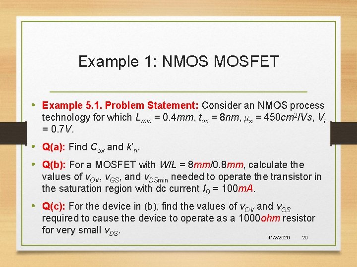
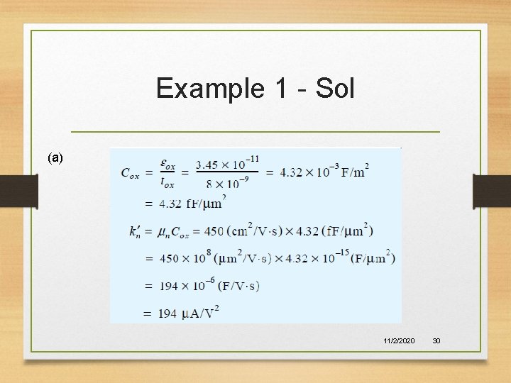
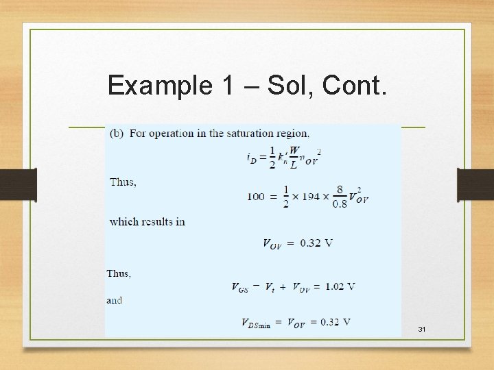
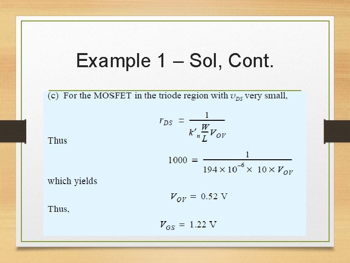
Example 1: NMOS MOSFET • Example 5. 1. Problem Statement: Consider an NMOS process technology for which Lmin = 0. 4 mm, tox = 8 nm, μn = 450 cm 2/Vs, Vt = 0. 7 V. • Q(a): Find Cox and k’n. • Q(b): For a MOSFET with W/L = 8 mm/0. 8 mm, calculate the values of v. OV, v. GS, and v. DSmin needed to operate the transistor in the saturation region with dc current ID = 100 m. A. • Q(c): For the device in (b), find the values of v. OV and v. GS required to cause the device to operate as a 1000 ohm resistor for very small v. DS. 11/2/2020 29

Example 1 - Sol (a) 11/2/2020 30

Example 1 – Sol, Cont. 11/2/2020 31

Example 1 – Sol, Cont. 11/2/2020 32

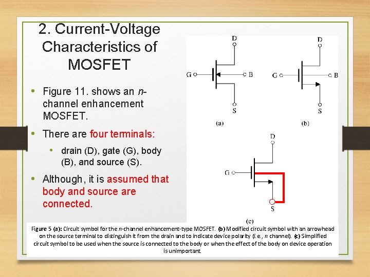
2. Current-Voltage Characteristics of MOSFET • Figure 11. shows an nchannel enhancement MOSFET. • There are four terminals: • drain (D), gate (G), body (B), and source (S). • Although, it is assumed that body and source are connected. Figure 5 (a): Circuit symbol for the n-channel enhancement-type MOSFET. (b) Modified circuit symbol with an arrowhead on the source terminal to distinguish it from the drain and to indicate device polarity (i. e. , n channel). (c) Simplified circuit symbol to be used when the source is connected to the body or when the effect of the body 11/2/2020 on device operation 33 is unimportant.

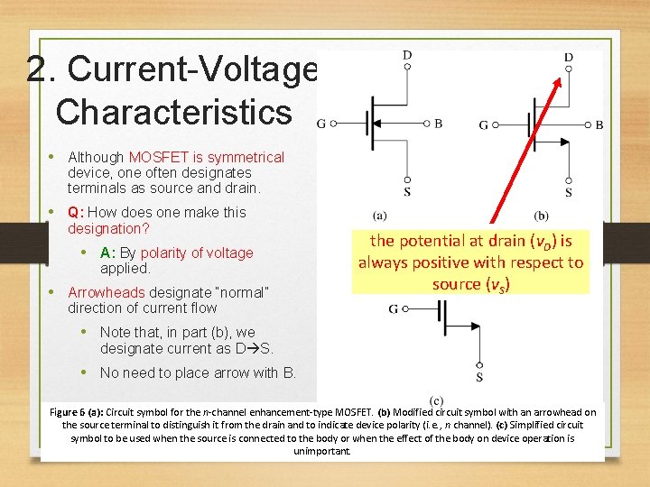
2. Current-Voltage Characteristics • Although MOSFET is symmetrical device, one often designates terminals as source and drain. • Q: How does one make this designation? • A: By polarity of voltage applied. • Arrowheads designate “normal” the potential at drain (v. D) is always positive with respect to source (v. S) direction of current flow • Note that, in part (b), we designate current as D S. • No need to place arrow with B. Figure 6 (a): Circuit symbol for the n-channel enhancement-type MOSFET. (b) Modified circuit symbol with an arrowhead on the source terminal to distinguish it from the drain and to indicate device polarity (i. e. , n channel). (c) Simplified circuit 34 symbol to be used when the source is connected to the body or when the effect of the body on 11/2/2020 device operation is unimportant.

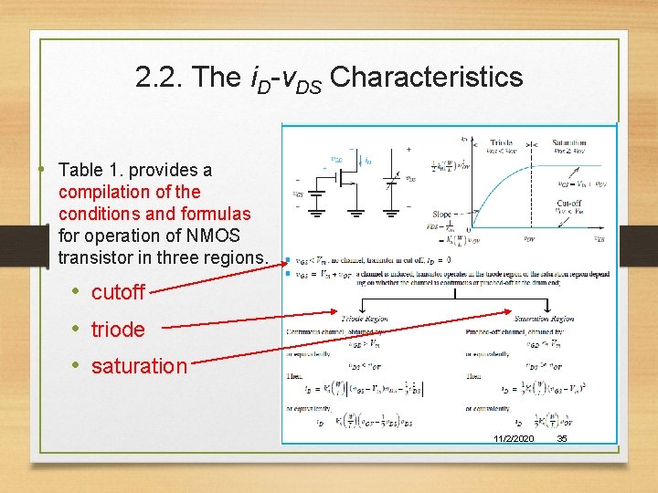
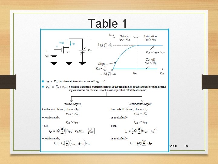
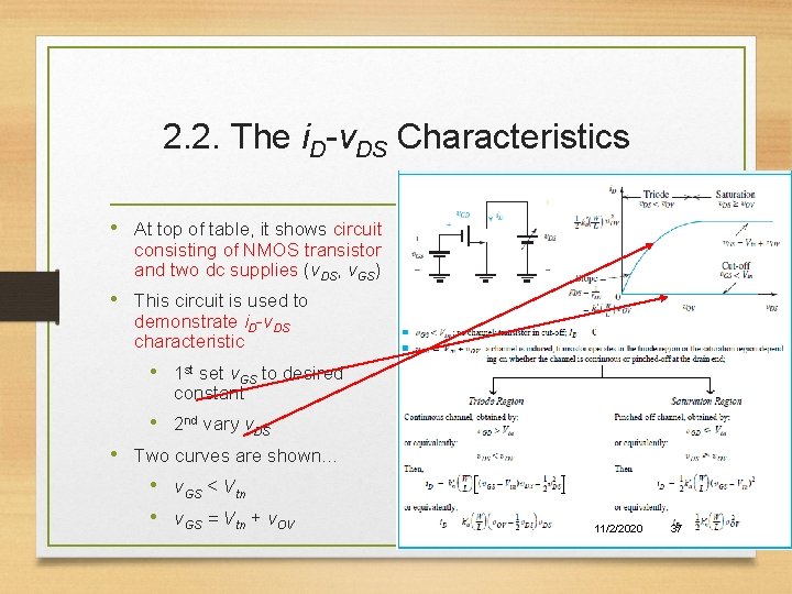
2. 2. The i. D-v. DS Characteristics • Table 1. provides a compilation of the conditions and formulas for operation of NMOS transistor in three regions. • cutoff • triode • saturation 11/2/2020 35

Table 1 11/2/2020 36

2. 2. The i. D-v. DS Characteristics • At top of table, it shows circuit consisting of NMOS transistor and two dc supplies (v. DS, v. GS) • This circuit is used to demonstrate i. D-v. DS characteristic • 1 st set v. GS to desired constant • 2 nd vary v. DS • Two curves are shown… • v. GS < Vtn • v. GS = Vtn + v. OV 11/2/2020 37

equation (7) as v. GS increases, so do the (1) saturation current and (2) beginning of the saturation region 11/2/2020 38 Figure 7: The i. D – v. DS characteristics for an enhancement-type NMOS transistor

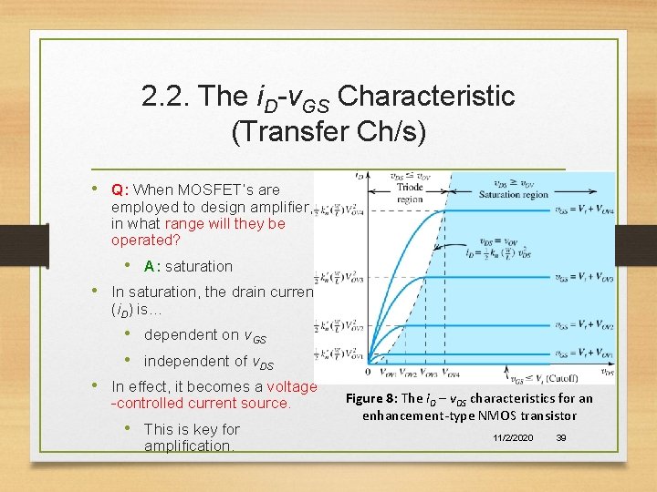
2. 2. The i. D-v. GS Characteristic (Transfer Ch/s) • Q: When MOSFET’s are employed to design amplifier, in what range will they be operated? • A: saturation • In saturation, the drain current (i. D) is… • dependent on v. GS • independent of v. DS • In effect, it becomes a voltage -controlled current source. • This is key for amplification. Figure 8: The i. D – v. DS characteristics for an enhancement-type NMOS transistor 11/2/2020 39

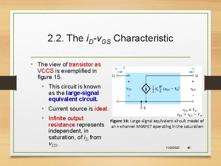
2. 2. The i. D-v. GS Characteristic • The view of transistor as VCCS is exemplified in figure 15. • This circuit is known as the large-signal equivalent circuit. • Current source is ideal. • Infinite output Figure 10: Large-signal equivalent-circuit model of resistance represents independent, in saturation, of i. D from v. DS. . an n-channel MOSFET operating in the saturation 11/2/2020 40

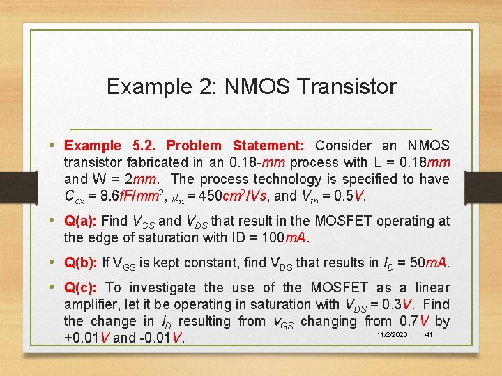
Example 2: NMOS Transistor • Example 5. 2. Problem Statement: Consider an NMOS transistor fabricated in an 0. 18 -mm process with L = 0. 18 mm and W = 2 mm. The process technology is specified to have Cox = 8. 6 f. F/mm 2, μn = 450 cm 2/Vs, and Vtn = 0. 5 V. • Q(a): Find VGS and VDS that result in the MOSFET operating at the edge of saturation with ID = 100 m. A. • Q(b): If VGS is kept constant, find VDS that results in ID = 50 m. A. • Q(c): To investigate the use of the MOSFET as a linear amplifier, let it be operating in saturation with VDS = 0. 3 V. Find the change in i. D resulting from v. GS changing from 0. 7 V by 11/2/2020 41 +0. 01 V and -0. 01 V.

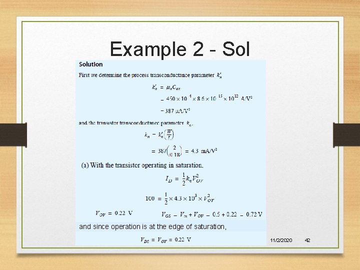
Example 2 - Sol and since operation is at the edge of saturation, 11/2/2020 42

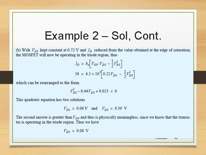
Example 2 – Sol, Cont. 11/2/2020 43

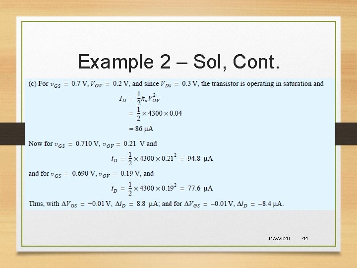
Example 2 – Sol, Cont. 11/2/2020 44

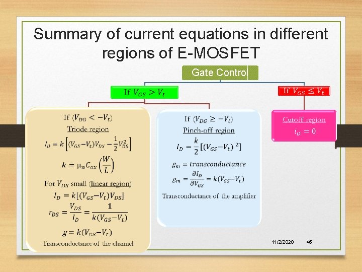
Summary of current equations in different regions of E-MOSFET Gate Control 11/2/2020 45

Summary • The enhancement-type MOSFET is current the modt widely used semiconductor device. It is the basis of CMOS technology, which is the most popular IC fabrication technology at this time. CMOS provides both n-channel (NMOS) and p-channel (PMOS) transistors, which increases design flexibility. The minimum MOSFET channel length achievable with a given CMOS process is used to characterize the process • The overdrive voltage |VOV| = |VGS| - |Vt| is the key quantity that governs the operation of the MOSFET. For amplifier applications, the MOSFET must operate in the saturation region. 11/2/2020 46

Summary • In saturation, i. D shows some linear dependence on v. DS as a result of the change in channel length. This channel-length modulation phenomenon becomes more pronounced as L decreases. It is modeled by ascribing an output resistance ro = |VA|/ID to the MOSFET model. Although the effect of ro on the operation of discrete-circuit MOS amplifiers is small, that is not the case in IC amplifiers. • The essence of the use of MOSFET as an amplifier is that in saturation v. GS controls i. D in the manner of a voltage-controller current source. When the device is dc biased in the saturation region, a small-signal input (vgs) may be amplified 11/2/2020 47 linearly.