CCE 201 Solid State Electronic Devices EEC 223
- Slides: 61

CCE 201: Solid State Electronic Devices EEC 223: Electronics (1) Lecture 05: Diodes Applications & Special diode types Prepared By Dr. Eng. Sherif Hekal Assistant Professor, CCE department Lecture 01 11/21/2020 1

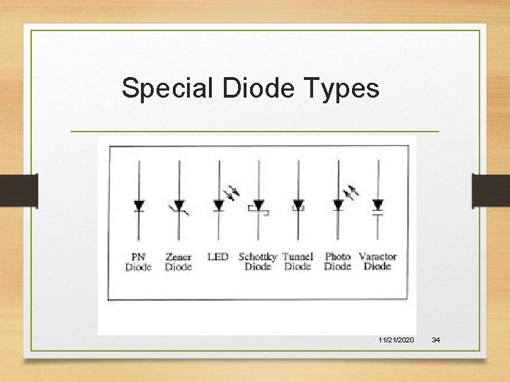
Introduction • In this Lecture we will learn q application of the diode in the design of rectifier circuits, which convert ac voltages to dc as needed for powering electronic equipment. q a number of other practical and important applications: limiting and clamping circuits. q Special diode types: LED, Photo diode, Schottky diode, Varactor diode, Zener diode. 11/21/2020 2

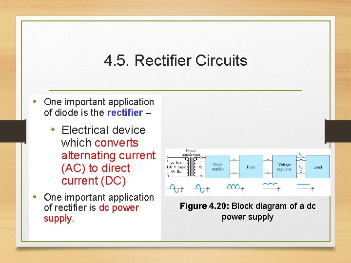
4. 5. Rectifier Circuits • One important application of diode is the rectifier – • Electrical device which converts alternating current (AC) to direct current (DC) • One important application of rectifier is dc power supply. Figure 4. 20: Block diagram of a dc power supply

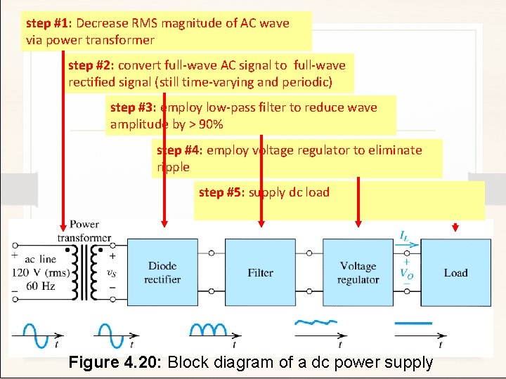
step #1: Decrease RMS magnitude of AC wave via power transformer step #2: convert full-wave AC signal to full-wave rectified signal (still time-varying and periodic) step #3: employ low-pass filter to reduce wave amplitude by > 90% step #4: employ voltage regulator to eliminate ripple step #5: supply dc load. Oxford University Publishing Microelectronic Circuits by Adel S. Sedra and Kenneth C. Smith (0195323033) Figure 4. 20: Block diagram of a dc power supply

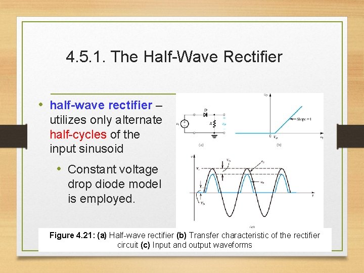
4. 5. 1. The Half-Wave Rectifier • half-wave rectifier – utilizes only alternate half-cycles of the input sinusoid • Constant voltage drop diode model is employed. Figure 4. 21: (a) Half-wave rectifier (b) Transfer characteristic of the rectifier 11/21/2020 5 circuit (c) Input and output waveforms

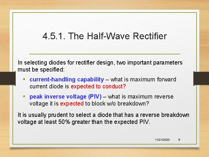
4. 5. 1. The Half-Wave Rectifier In selecting diodes for rectifier design, two important parameters must be specified: • current-handling capability – what is maximum forward current diode is expected to conduct? • peak inverse voltage (PIV) – what is maximum reverse voltage it is expected to block w/o breakdown? It is usually prudent to select a diode that has a reverse breakdown voltage at least 50% greater than the expected PIV. 11/21/2020 6

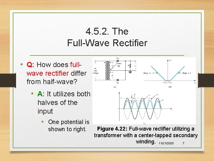
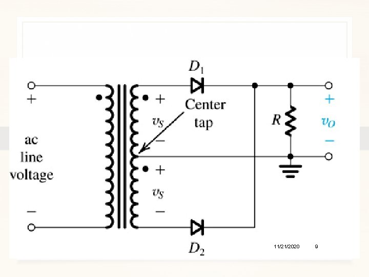
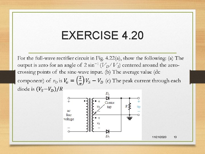
4. 5. 2. The Full-Wave Rectifier • Q: How does fullwave rectifier differ from half-wave? • A: It utilizes both halves of the input • One potential is shown to right. Figure 4. 22: Full-wave rectifier utilizing a transformer with a center-tapped secondary winding. 11/21/2020 7

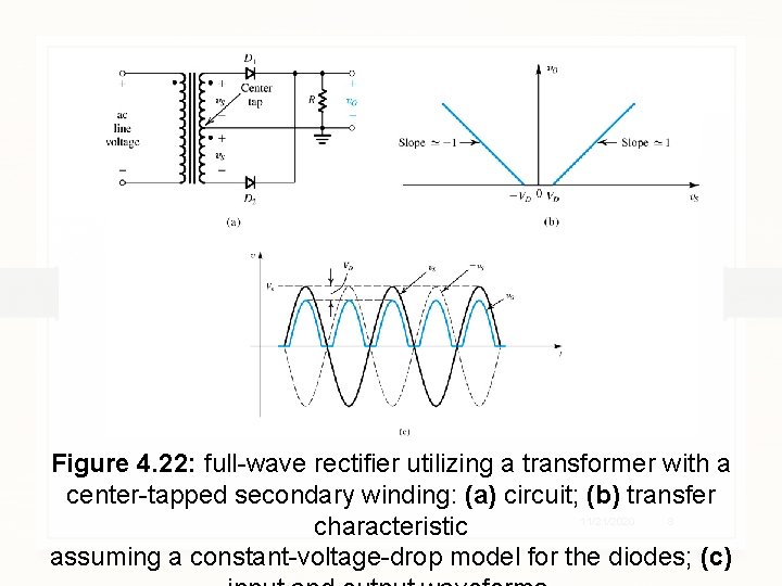
Figure 4. 22: full-wave rectifier utilizing a transformer with a center-tapped secondary winding: (a) circuit; (b) transfer 11/21/2020 8 characteristic assuming a constant-voltage-drop model for the diodes; (c)

11/21/2020 9

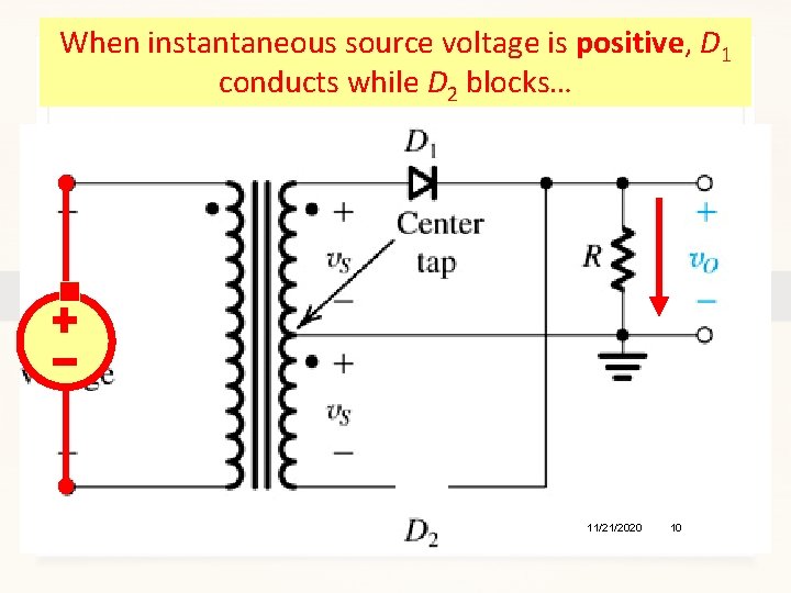
When instantaneous source voltage is positive, D 1 conducts while D 2 blocks… 11/21/2020 10

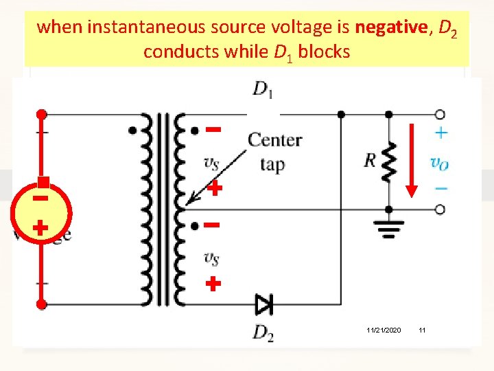
when instantaneous source voltage is negative, D 2 conducts while D 1 blocks 11/21/2020 11

4. 5. 2. The Full-Wave Rectifier • Q: What are most important observation(s) from this operation? • A: The direction of current flowing across load never changes (both halves of AC wave are rectified). The full-wave rectifier produces a more “energetic” waveform than half-wave. • PIV for full-wave = 2 VS – VD 11/21/2020 12

EXERCISE 4. 20 11/21/2020 13

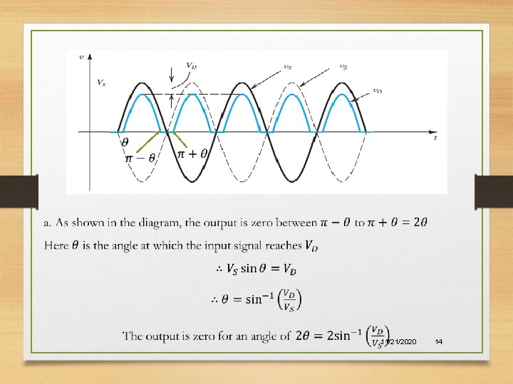
EXERCISE 4. 20 11/21/2020 14

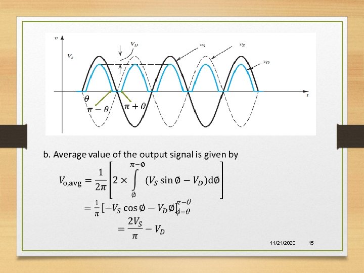
EXERCISE 4. 20 11/21/2020 15

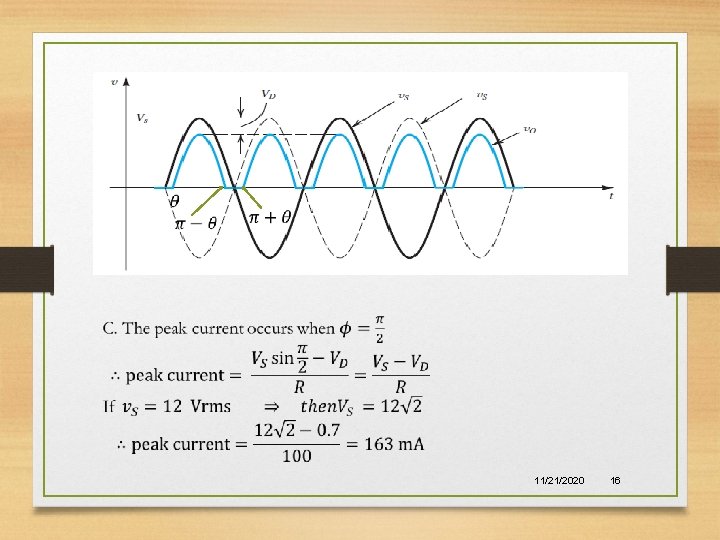
EXERCISE 4. 20 11/21/2020 16

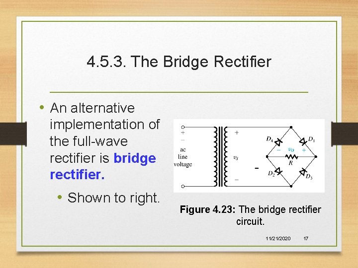
4. 5. 3. The Bridge Rectifier • An alternative implementation of the full-wave rectifier is bridge rectifier. • Shown to right. Figure 4. 23: The bridge rectifier circuit. 11/21/2020 17

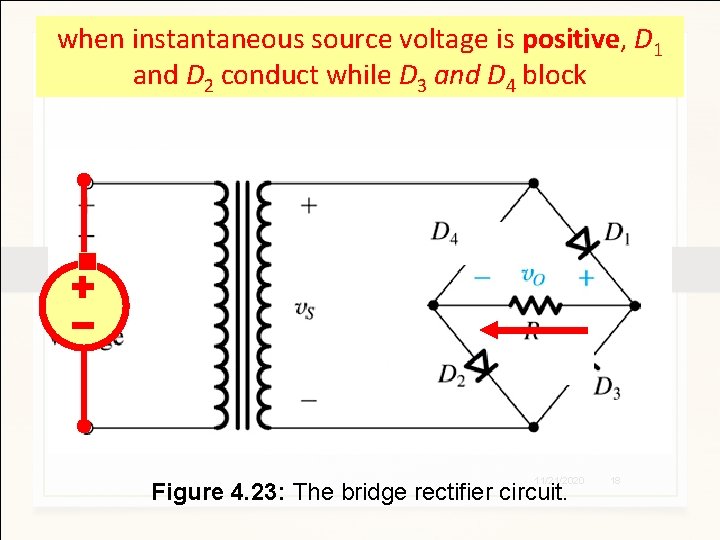
when instantaneous source voltage is positive, D 1 and D 2 conduct while D 3 and D 4 block 11/21/2020 Figure 4. 23: The bridge rectifier circuit. 18

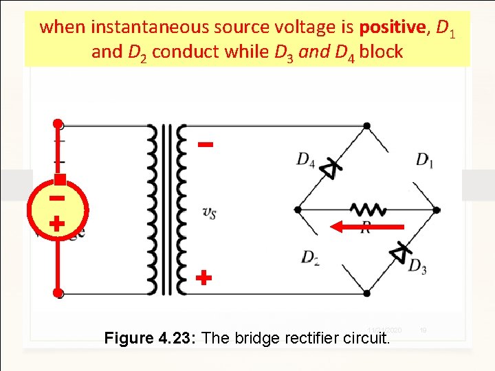
when instantaneous source voltage is positive, D 1 and D 2 conduct while D 3 and D 4 block 11/21/2020 Figure 4. 23: The bridge rectifier circuit. 19

4. 5. 3: The Bridge Rectifier (BR) • Q: What is the main advantage of BR? • A: No need for center-tapped transformer. • Q: What is main disadvantage? • A: Series connection of TWO diodes will reduce output voltage. • PIV = VS – VD 11/21/2020 20

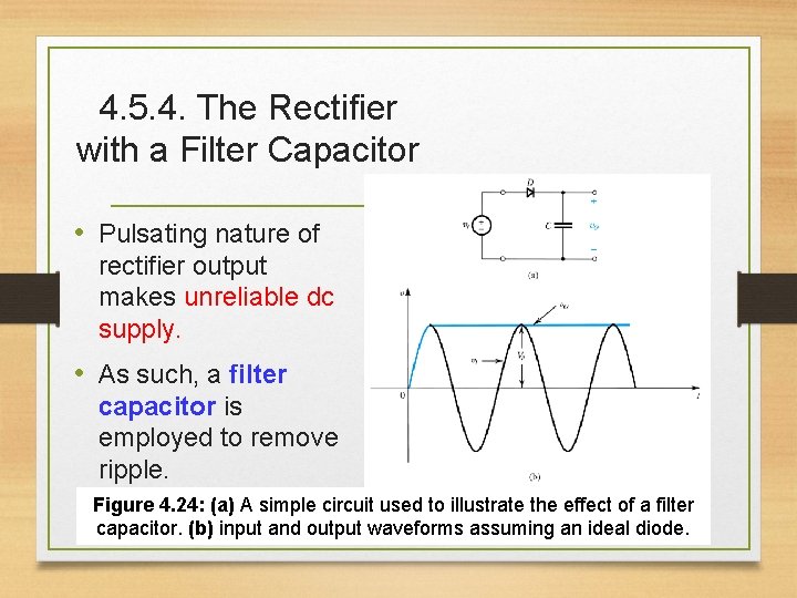
4. 5. 4. The Rectifier with a Filter Capacitor • Pulsating nature of rectifier output makes unreliable dc supply. • As such, a filter capacitor is employed to remove ripple. Figure 4. 24: (a) A simple circuit used to illustrate the effect of a filter capacitor. (b) input and output waveforms assuming an ideal diode. 11/21/2020 21

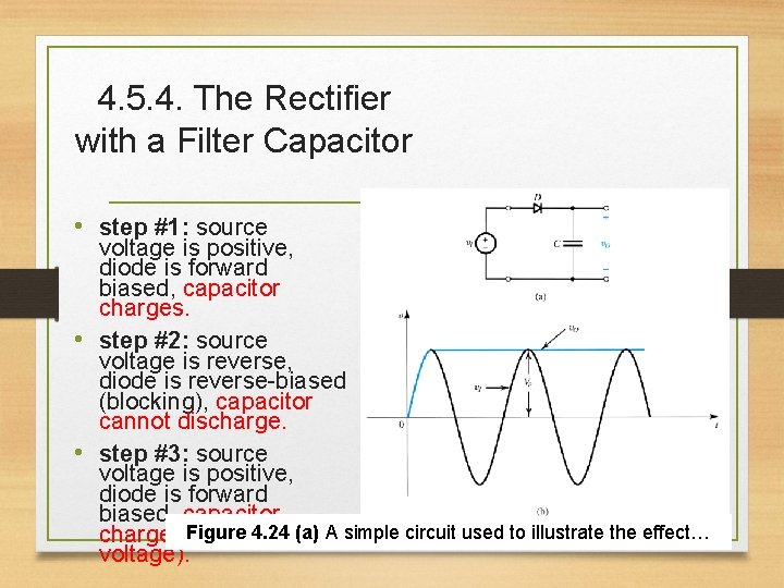
4. 5. 4. The Rectifier with a Filter Capacitor • step #1: source voltage is positive, diode is forward biased, capacitor charges. • step #2: source voltage is reverse, diode is reverse-biased (blocking), capacitor cannot discharge. • step #3: source voltage is positive, diode is forward biased, capacitor 11/21/2020 22 Figure 4. 24 (a) A simple circuit used to illustrate the effect… charges (maintains voltage).

4. 5. 4. The Rectifier with a Filter Capacitor • Q: Why is this example unrealistic? • A: Because for any practical application, the converter would supply a load (which in turn provides a path for capacitor discharging). 11/21/2020 23

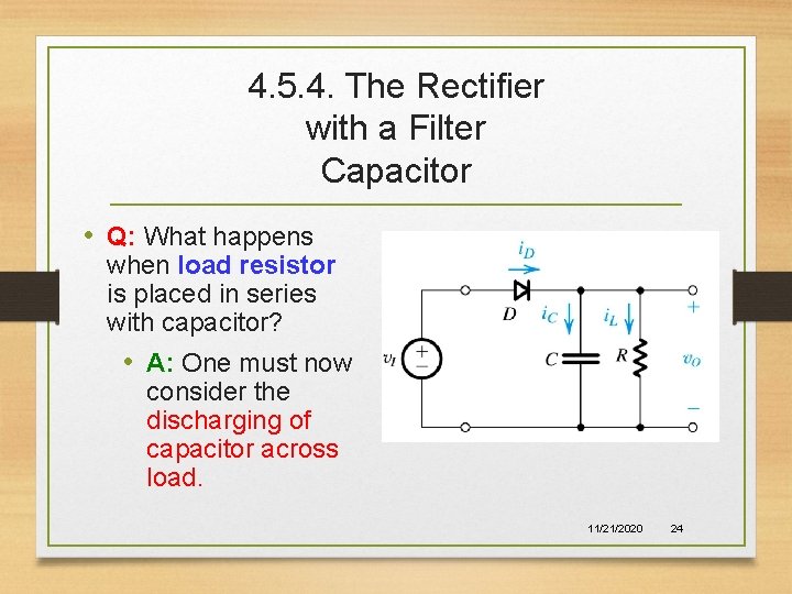
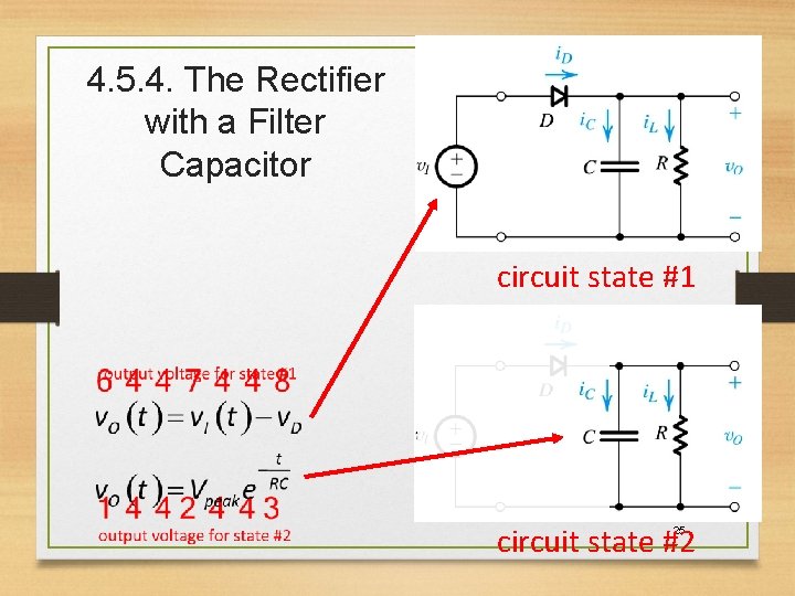
4. 5. 4. The Rectifier with a Filter Capacitor • Q: What happens when load resistor is placed in series with capacitor? • A: One must now consider the discharging of capacitor across load. 11/21/2020 24

4. 5. 4. The Rectifier with a Filter Capacitor circuit state #1 circuit state #2 25

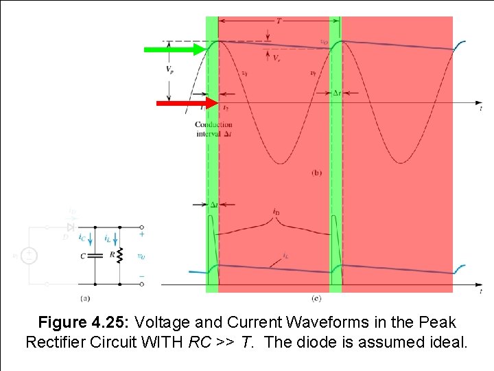
Figure 4. 25: Voltage and Current Waveforms in the Peak 11/21/2020 26 Rectifier Circuit WITH RC >> T. The diode is assumed ideal.

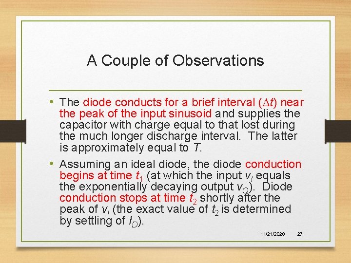
A Couple of Observations • The diode conducts for a brief interval (Dt) near the peak of the input sinusoid and supplies the capacitor with charge equal to that lost during the much longer discharge interval. The latter is approximately equal to T. • Assuming an ideal diode, the diode conduction begins at time t 1 (at which the input v. I equals the exponentially decaying output v. O). Diode conduction stops at time t 2 shortly after the peak of v. I (the exact value of t 2 is determined by settling of ID). 11/21/2020 27

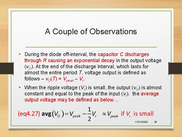
A Couple of Observations • During the diode off-interval, the capacitor C discharges through R causing an exponential decay in the output voltage (v. O). At the end of the discharge interval, which lasts for almost the entire period T, voltage output is defined as follows – v. O(T) = Vpeak – Vr. • When the ripple voltage (Vr) is small, the output (v. O) is almost constant and equal to the peak of the input (v. I). the average output voltage may be defined as below… 11/21/2020 28

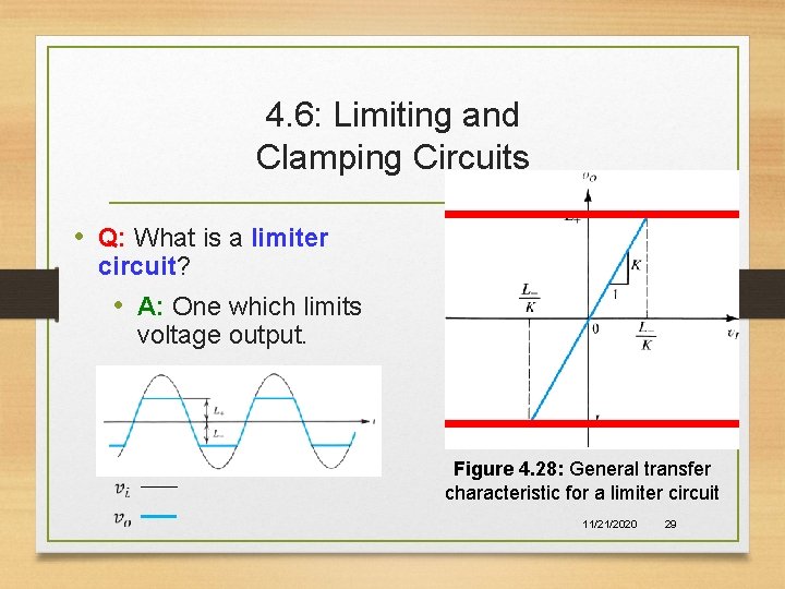
4. 6: Limiting and Clamping Circuits • Q: What is a limiter circuit? • A: One which limits voltage output. Figure 4. 28: General transfer characteristic for a limiter circuit 11/21/2020 29

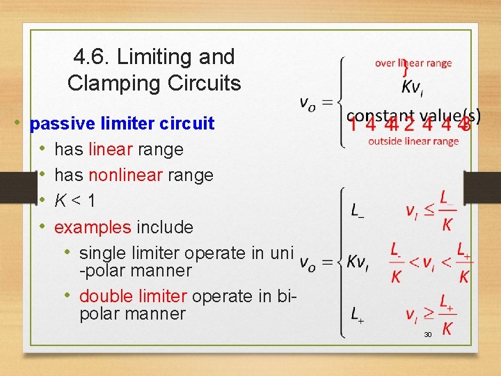
4. 6. Limiting and Clamping Circuits • passive limiter circuit • has linear range • has nonlinear range • K < 1 • examples include • single limiter operate in uni -polar manner • double limiter operate in bipolar manner 30

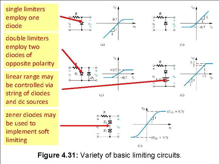
single limiters employ one diode double limiters employ two diodes of opposite polarity linear range may be controlled via string of diodes and dc sources zener diodes may be used to implement soft limiting 11/21/2020 Figure 4. 31: Variety of basic limiting circuits. 31

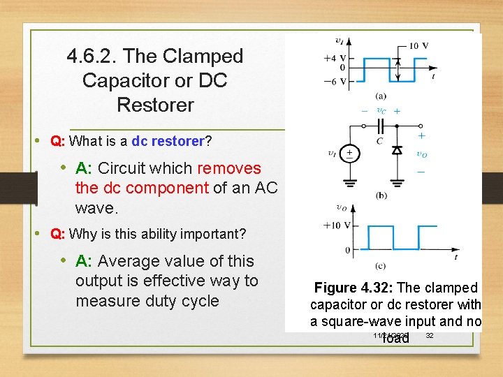
4. 6. 2. The Clamped Capacitor or DC Restorer • Q: What is a dc restorer? • A: Circuit which removes the dc component of an AC wave. • Q: Why is this ability important? • A: Average value of this output is effective way to measure duty cycle Figure 4. 32: The clamped capacitor or dc restorer with a square-wave input and no 11/21/2020 load 32

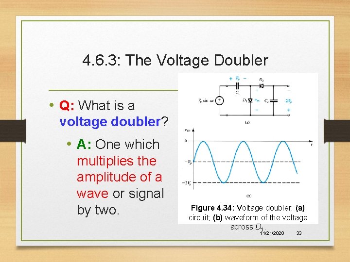
4. 6. 3: The Voltage Doubler • Q: What is a voltage doubler? • A: One which multiplies the amplitude of a wave or signal by two. Figure 4. 34: Voltage doubler: (a) circuit; (b) waveform of the voltage across D 1. 11/21/2020 33

Special Diode Types 11/21/2020 34

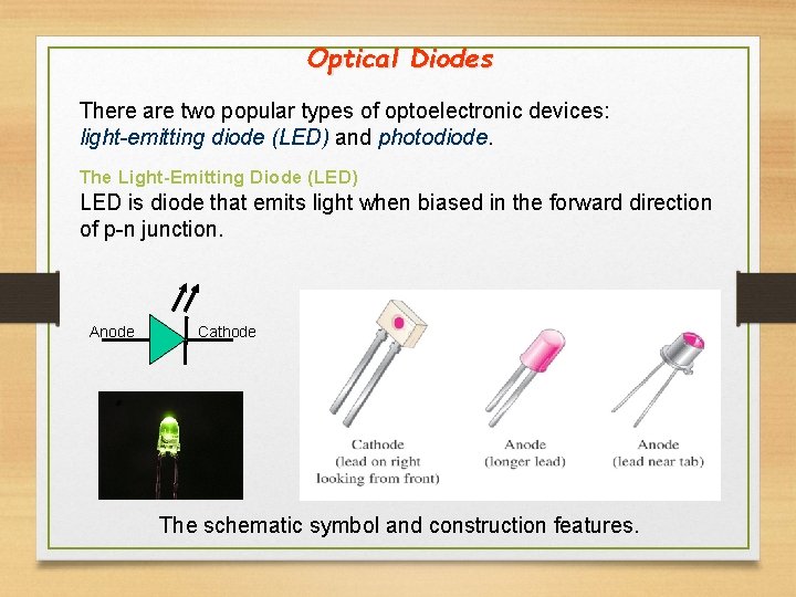
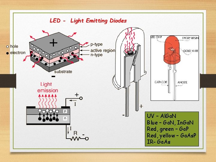
Optical Diodes There are two popular types of optoelectronic devices: light-emitting diode (LED) and photodiode. The Light-Emitting Diode (LED) LED is diode that emits light when biased in the forward direction of p-n junction. Anode Cathode The schematic symbol and construction features.

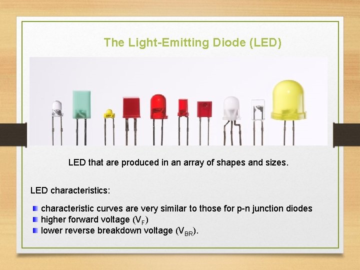
The Light-Emitting Diode (LED) LED that are produced in an array of shapes and sizes. LED characteristics: characteristic curves are very similar to those for p-n junction diodes higher forward voltage (VF) lower reverse breakdown voltage (VBR).

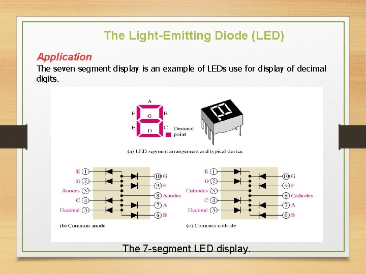
The Light-Emitting Diode (LED) Application The seven segment display is an example of LEDs use for display of decimal digits. The 7 -segment LED display.

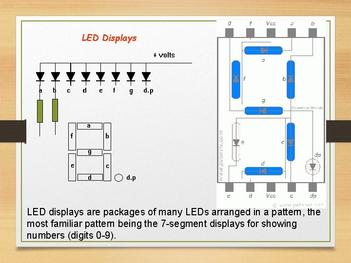
LED Displays LED displays are packages of many LEDs arranged in a pattern, the most familiar pattern being the 7 -segment displays for showing numbers (digits 0 -9).

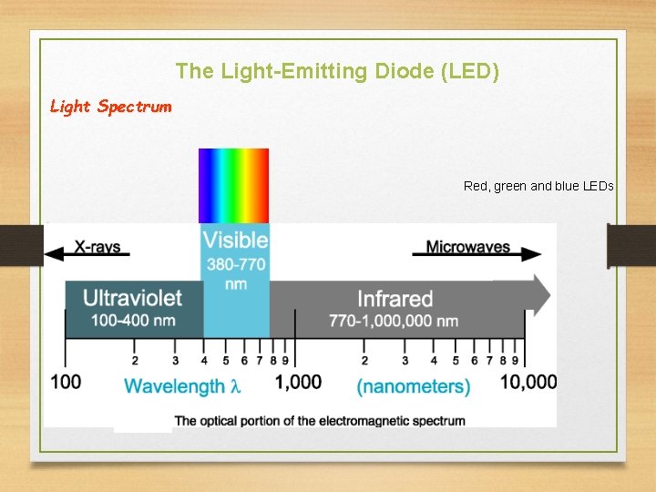
The Light-Emitting Diode (LED) Light Spectrum Red, green and blue LEDs

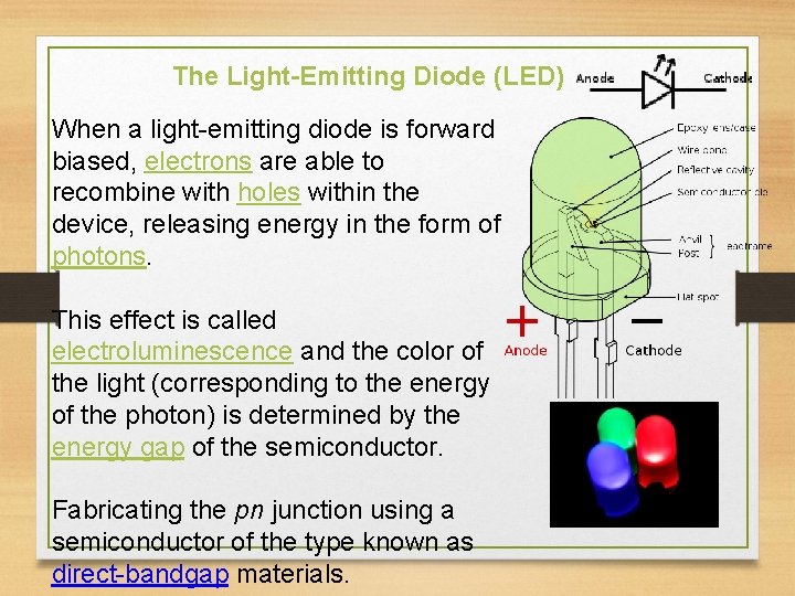
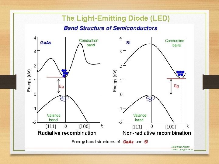
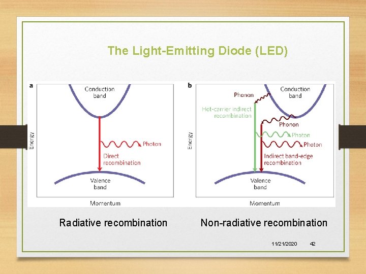
The Light-Emitting Diode (LED) When a light-emitting diode is forward biased, electrons are able to recombine with holes within the device, releasing energy in the form of photons. This effect is called electroluminescence and the color of the light (corresponding to the energy of the photon) is determined by the energy gap of the semiconductor. Fabricating the pn junction using a semiconductor of the type known as direct-bandgap materials.

The Light-Emitting Diode (LED) Radiative recombination Non-radiative recombination 11/21/2020 41

The Light-Emitting Diode (LED) Radiative recombination Non-radiative recombination 11/21/2020 42

LED - Light Emitting Diodes UV – Al. Ga. N Blue – Ga. N, In. Ga. N Red, green – Ga. P Red, yellow – Ga. As. P IR- Ga. As

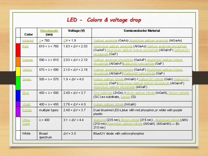
LED - Colors & voltage drop Color Wavelength (nm) Voltage (V) Semiconductor Material Infrared λ > 760 ΔV < 1. 9 Gallium arsenide (Ga. As) Aluminium gallium arsenide (Al. Ga. As) Red 610 < λ < 760 1. 63 < ΔV < 2. 03 Aluminium gallium arsenide (Al. Ga. As) Gallium arsenide phosphide (Ga. As. P) Aluminium gallium indium phosphide (Al. Ga. In. P) Gallium(III) phosphide (Ga. P) Orange 590 < λ < 610 2. 03 < ΔV < 2. 10 Gallium arsenide phosphide (Ga. As. P) Aluminium gallium indium phosphide (Al. Ga. In. P)Gallium(III) phosphide (Ga. P) Yellow 570 < λ < 590 2. 10 < ΔV < 2. 18 Gallium arsenide phosphide (Ga. As. P) Aluminium gallium indium phosphide (Al. Ga. In. P) Gallium(III) phosphide (Ga. P) Green 500 < λ < 570 1. 9 < ΔV < 4. 0 Indium gallium nitride (In. Ga. N) / Gallium(III) nitride (Ga. N) Gallium(III) phosphide (Ga. P)Aluminium gallium indium phosphide (Al. Ga. In. P) Aluminium gallium phosphide (Al. Ga. P) Blue 450 < λ < 500 2. 48 < ΔV < 3. 7 Zinc selenide (Zn. Se), Indium gallium nitride (In. Ga. N), Silicon carbide (Si. C) as substrate, Silicon (Si) Violet 400 < λ < 450 2. 76 < ΔV < 4. 0 Indium gallium nitride (In. Ga. N) Purple multiple types 2. 48 < ΔV < 3. 7 Dual blue/red LEDs, blue with red phosphor, or white with purple plastic Ultraviolet λ < 400 3. 1 < ΔV < 4. 4 diamond (235 nm), Boron nitride (215 nm) , Aluminium nitride (Al. N) (210 nm) Aluminium gallium nitride (Al. Ga. N) (Al. Ga. In. N) — (to 210 nm) White Broad spectrum ΔV = 3. 5 Blue/UV diode with yellow phosphor

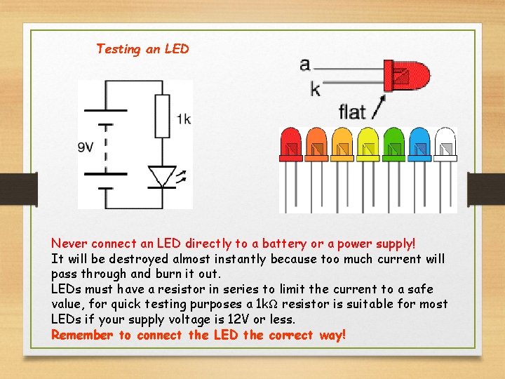
Testing an LED Never connect an LED directly to a battery or a power supply! It will be destroyed almost instantly because too much current will pass through and burn it out. LEDs must have a resistor in series to limit the current to a safe value, for quick testing purposes a 1 kΩ resistor is suitable for most LEDs if your supply voltage is 12 V or less. Remember to connect the LED the correct way!

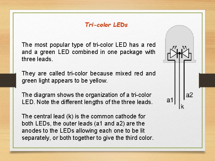
Tri-color LEDs The most popular type of tri-color LED has a red and a green LED combined in one package with three leads. They are called tri-color because mixed red and green light appears to be yellow. The diagram shows the organization of a tri-color LED. Note the different lengths of the three leads. The central lead (k) is the common cathode for both LEDs, the outer leads (a 1 and a 2) are the anodes to the LEDs allowing each one to be lit separately, or both together to give third color.

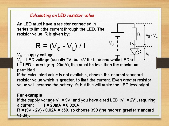
Calculating an LED resistor value An LED must have a resistor connected in series to limit the current through the LED. The resistor value, R is given by: R = (VS - VL) / I VS = supply voltage VL = LED voltage (usually 2 V, but 4 V for blue and white LEDs) I = LED current (e. g. 20 m. A), this must be less than the maximum permitted If the calculated value is not available, choose the nearest standard resistor value which is greater, to limit the current. Even greater resistor value will increase the battery life but this will make the LED less bright. For example If the supply voltage VS = 9 V, and you have a red LED (VL = 2 V), requiring a current I = 20 m. A = 0. 020 A, R = (9 V - 2 V) / 0. 02 A = 350, so choose 390 (the nearest greater standard value).

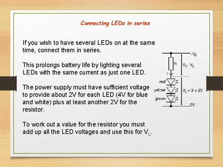
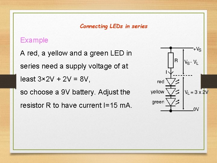
Connecting LEDs in series If you wish to have several LEDs on at the same time, connect them in series. This prolongs battery life by lighting several LEDs with the same current as just one LED. The power supply must have sufficient voltage to provide about 2 V for each LED (4 V for blue and white) plus at least another 2 V for the resistor. To work out a value for the resistor you must add up all the LED voltages and use this for VL.

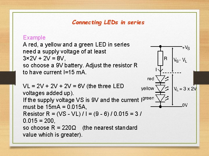
Connecting LEDs in series Example A red, a yellow and a green LED in series need a supply voltage of at least 3× 2 V + 2 V = 8 V, so choose a 9 V battery. Adjust the resistor R to have current I=15 m. A.

Connecting LEDs in series Example A red, a yellow and a green LED in series need a supply voltage of at least 3× 2 V + 2 V = 8 V, so choose a 9 V battery. Adjust the resistor R to have current I=15 m. A. VL = 2 V + 2 V = 6 V (the three LED voltages added up). If the supply voltage VS is 9 V and the current I must be 15 m. A = 0. 015 A, Resistor R = (VS - VL) / I = (9 - 6) / 0. 015 = 3 / 0. 015 = 200, so choose R = 220Ω (the nearest standard value which is greater).

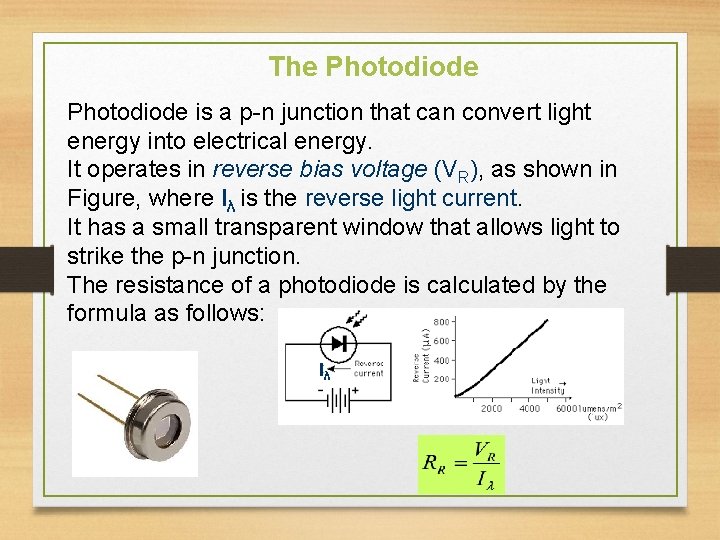
The Photodiode is a p-n junction that can convert light energy into electrical energy. It operates in reverse bias voltage (VR), as shown in Figure, where Iλ is the reverse light current. It has a small transparent window that allows light to strike the p-n junction. The resistance of a photodiode is calculated by the formula as follows: Iλ

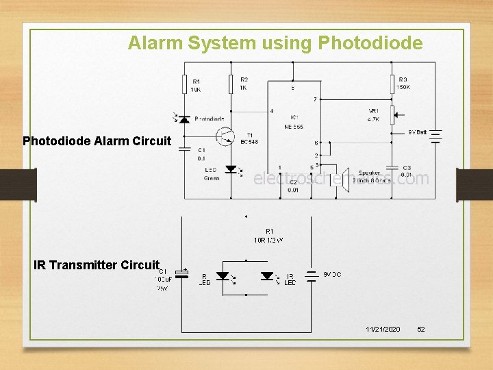
Alarm System using Photodiode Alarm Circuit IR Transmitter Circuit 11/21/2020 52

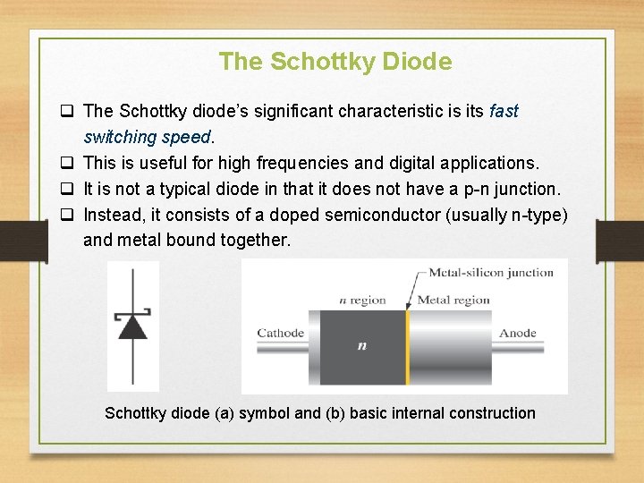
The Schottky Diode q The Schottky diode’s significant characteristic is its fast switching speed. q This is useful for high frequencies and digital applications. q It is not a typical diode in that it does not have a p-n junction. q Instead, it consists of a doped semiconductor (usually n-type) and metal bound together. Schottky diode (a) symbol and (b) basic internal construction

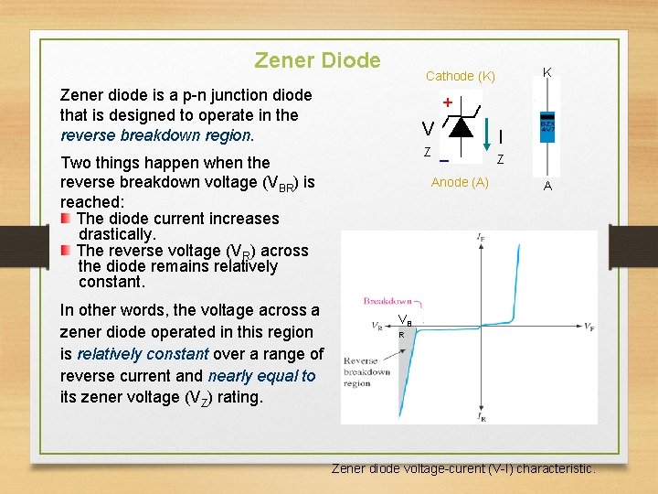
Zener Diode Zener diode is a p-n junction diode that is designed to operate in the reverse breakdown region. + V Z Two things happen when the reverse breakdown voltage (VBR) is reached: The diode current increases drastically. The reverse voltage (VR) across the diode remains relatively constant. In other words, the voltage across a zener diode operated in this region is relatively constant over a range of reverse current and nearly equal to its zener voltage (VZ) rating. K Cathode (K) I − Anode (A) Z A VB R Zener diode voltage-curent (V-I) characteristic.

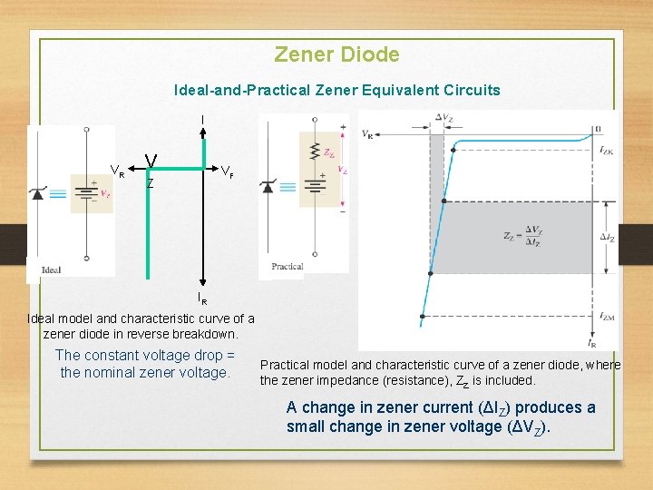
Zener Diode Ideal-and-Practical Zener Equivalent Circuits I F VR V VF Z IR Ideal model and characteristic curve of a zener diode in reverse breakdown. The constant voltage drop = the nominal zener voltage. Practical model and characteristic curve of a zener diode, where the zener impedance (resistance), ZZ is included. A change in zener current (ΔIZ) produces a small change in zener voltage (ΔVZ).

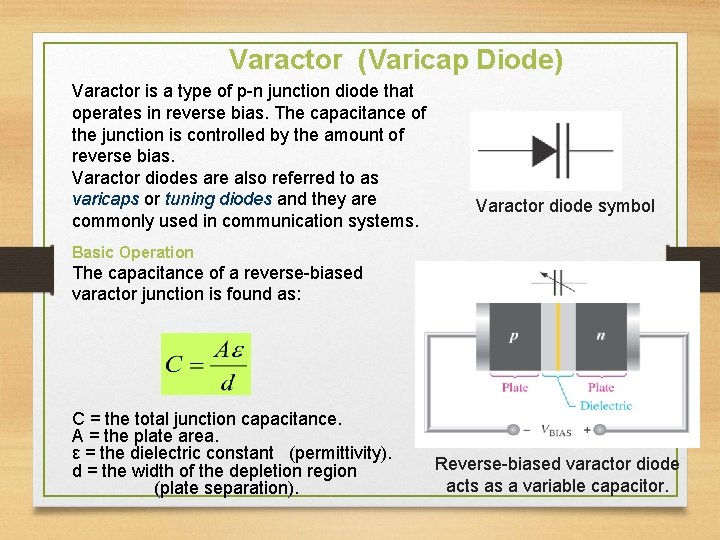
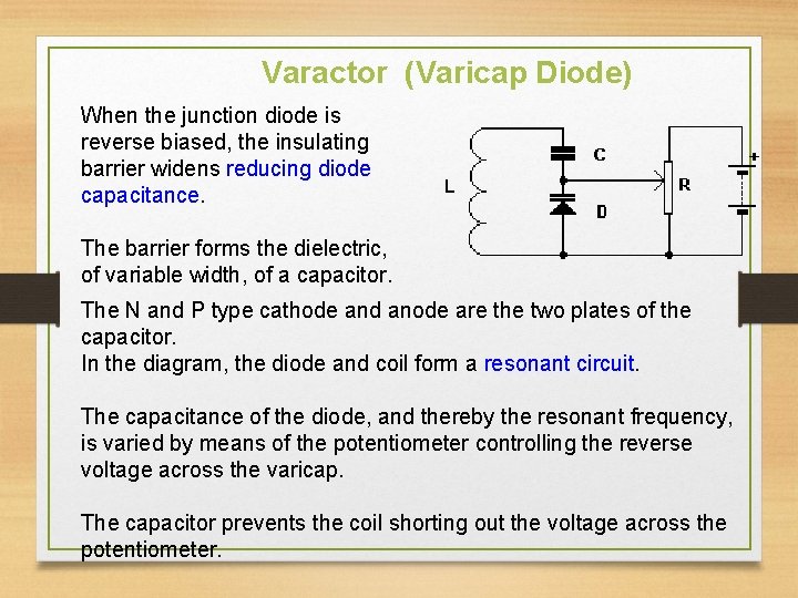
Varactor (Varicap Diode) Varactor is a type of p-n junction diode that operates in reverse bias. The capacitance of the junction is controlled by the amount of reverse bias. Varactor diodes are also referred to as varicaps or tuning diodes and they are commonly used in communication systems. Varactor diode symbol Basic Operation The capacitance of a reverse-biased varactor junction is found as: C = the total junction capacitance. A = the plate area. ε = the dielectric constant (permittivity). d = the width of the depletion region (plate separation). Reverse-biased varactor diode acts as a variable capacitor.

Varactor (Varicap Diode) When the junction diode is reverse biased, the insulating barrier widens reducing diode capacitance. The barrier forms the dielectric, of variable width, of a capacitor. The N and P type cathode and anode are the two plates of the capacitor. In the diagram, the diode and coil form a resonant circuit. The capacitance of the diode, and thereby the resonant frequency, is varied by means of the potentiometer controlling the reverse voltage across the varicap. The capacitor prevents the coil shorting out the voltage across the potentiometer.

Summary (1) • Rectifiers convert ac voltage into unipolar voltages. Half-wave rectifiers do this by passing the voltage in half of each cycle and blocking the opposite-polarity voltage in the other half of the cycle. • The bridge-rectifier circuit is the preferred fullwave rectifier configuration. 11/21/2020 58

Summary (2) • The variation of the output waveform of the rectifier is reduced considerably by connecting a capacitor C across the output load resistance R. The resulting circuit is the peak rectifier. The output waveform then consists of a dc voltage almost equal to the peak of the input sine wave, Vp, on which is superimposed a ripple component of frequency 2 f (in the full-wave case) and of peakto-peak amplitude Vr = Vp/2 f. RC. 11/21/2020 59

Summary (3) • Combination of diodes, resistors, and possible reference voltage can be used to design voltage limiters that prevent one or both extremities of the output waveform from going beyond predetermined values – the limiting levels. • Applying a time-varying waveform to a circuit consisting of a capacitor in series with a diode and taking the output across the diode provides a clamping function. 11/21/2020 • By cascading a clamping circuit with a peakrectifier circuit, a voltage doubler is realized. 60

Summary (4) • Beyond a certain value of reverse voltage (that depends on the diode itself), breakdown occurs and current increases rapidly with a small corresponding increase in voltage. • Diodes designed to operate in the breakdown region are called zener diodes. They are employed in the design of voltage regulators whose function is to provide a constant dc voltage that varies little with variations in power supply voltage and / or load current. 11/21/2020 61