CHAPTER 16 INTRODUCTION TO SEMICONDUCTORS ATOMIC STRUCTURE AND

- Slides: 29

CHAPTER 16 INTRODUCTION TO SEMICONDUCTORS

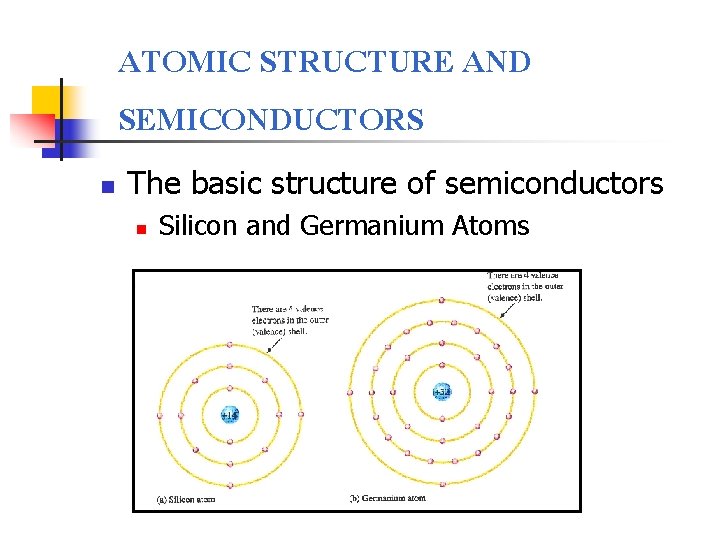
ATOMIC STRUCTURE AND SEMICONDUCTORS n The basic structure of semiconductors n Silicon and Germanium Atoms

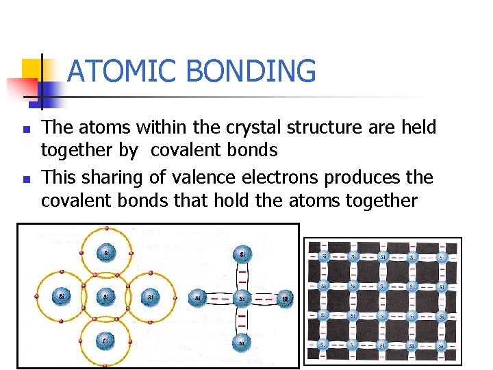
ATOMIC BONDING n n The atoms within the crystal structure are held together by covalent bonds This sharing of valence electrons produces the covalent bonds that hold the atoms together

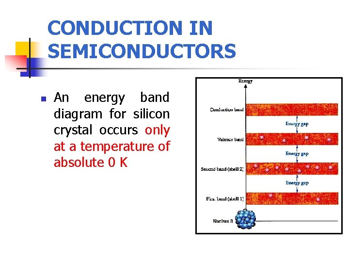
CONDUCTION IN SEMICONDUCTORS n An energy band diagram for silicon crystal occurs only at a temperature of absolute 0 K

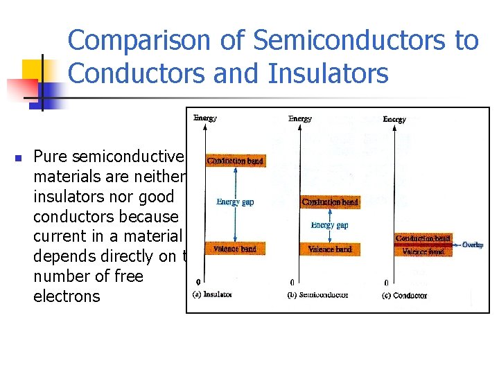
Comparison of Semiconductors to Conductors and Insulators n Pure semiconductive materials are neither insulators nor good conductors because current in a material depends directly on the number of free electrons

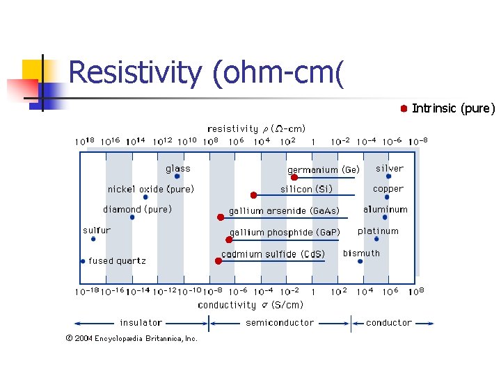
Resistivity (ohm-cm( Intrinsic (pure)

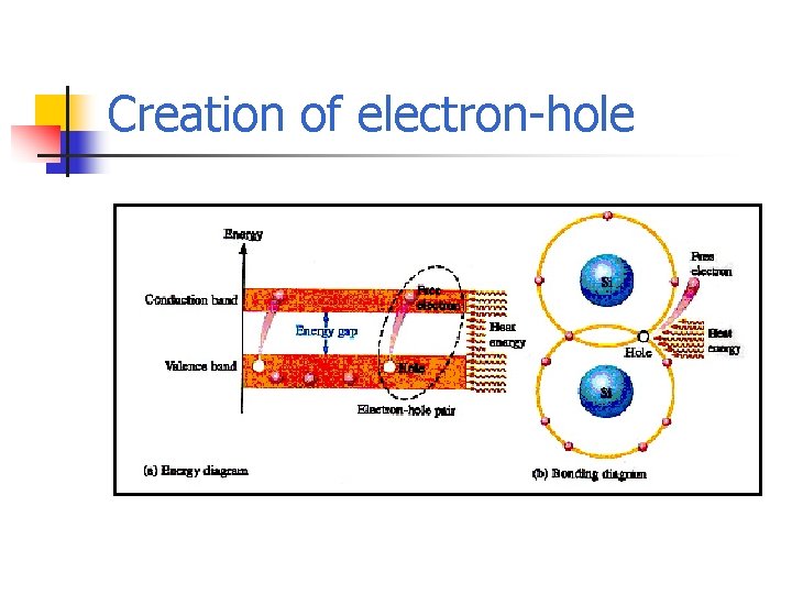
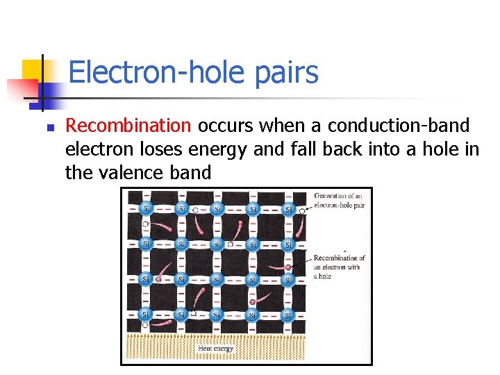
Conduction Electrons and Holes n n An intrinsic (pure) silicon crystal at room temperature has sufficient heat energy for some valence electrons to jump the gap from the valence band into the conduction band, which become free electrons When an electron jumps to the conduction band, a vacancy is left in the valence band within the crystal, called a hole.

Creation of electron-hole

Electron-hole pairs n Recombination occurs when a conduction-band electron loses energy and fall back into a hole in the valence band

l Types of Current in Semiconductor – Electron Current – Hole Current

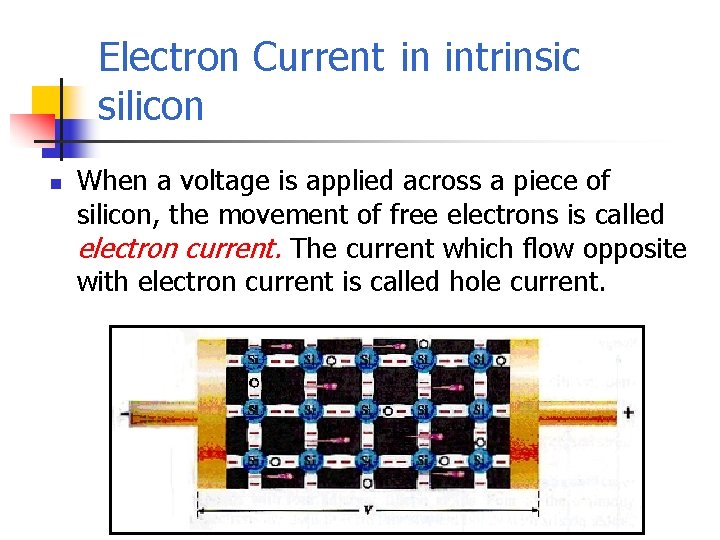
Electron Current in intrinsic silicon n When a voltage is applied across a piece of silicon, the movement of free electrons is called electron current. The current which flow opposite with electron current is called hole current.

Hole current in intrinsic silicon

N-TYPE AND P-TYPE SEMICONDUCTORS n n The conductivities of silicon and germanium can be increased and controlled by the addition of impurities to the intrinsic (pure) semiconductive material called doping The two categories of impurities are ntype and p-type

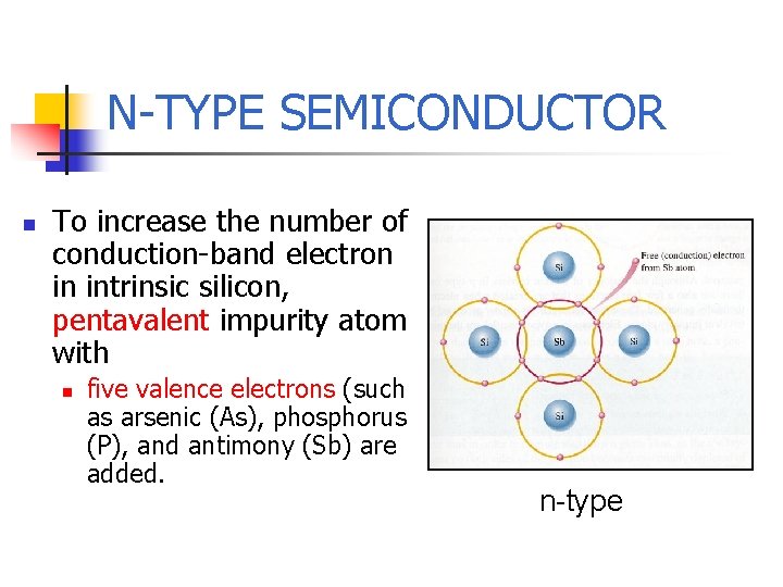
N-TYPE SEMICONDUCTOR n To increase the number of conduction-band electron in intrinsic silicon, pentavalent impurity atom with n five valence electrons (such as arsenic (As), phosphorus (P), and antimony (Sb) are added. n-type

Majority and Minority Carriers of N-type Semiconductor n n The electrons are called the majority carries in n-type material ( the n stand for the negative charge on an electron) Holes which are not produced by the addition of the pentavalent impurity atoms are called minority carries

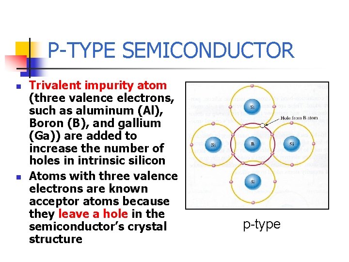
P-TYPE SEMICONDUCTOR n n Trivalent impurity atom (three valence electrons, such as aluminum (Al), Boron (B), and gallium (Ga)) are added to increase the number of holes in intrinsic silicon Atoms with three valence electrons are known acceptor atoms because they leave a hole in the semiconductor’s crystal structure p-type

Majority and Minority Carriers of P-type Semiconductor n n The holes are the majority carries in p-type material The Electron in p-type material are the minority carries

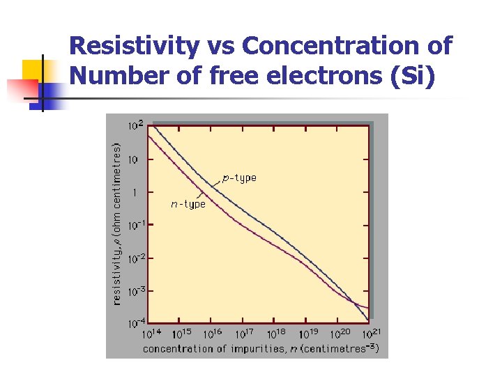
Resistivity vs Concentration of Number of free electrons (Si)

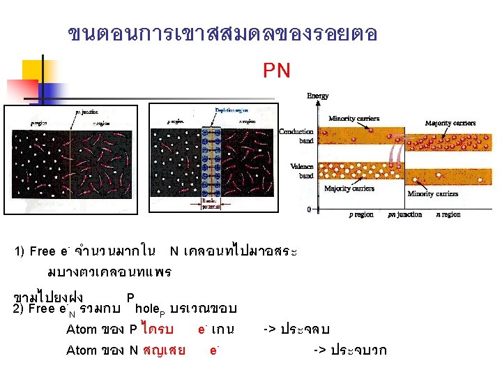
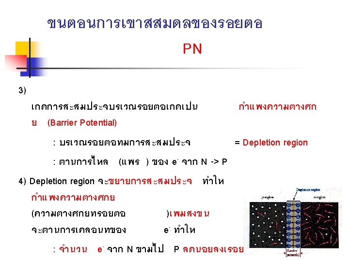
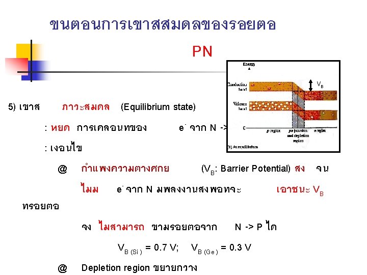
THE PN JUNCTION n n The junction of silicon which it has doped on one half with a trivalent impurity and the other half with a pentavalent impurity is called the pn junction The pn junction is the feature that allows diodes , transistor, and other devices to work


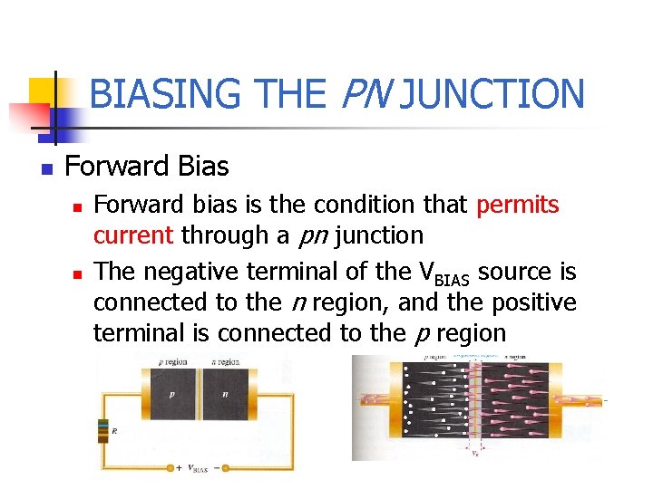
BIASING THE PN JUNCTION n Forward Bias n n Forward bias is the condition that permits current through a pn junction The negative terminal of the VBIAS source is connected to the n region, and the positive terminal is connected to the p region

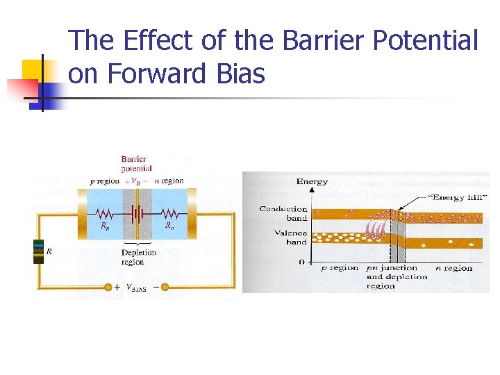
The Effect of the Barrier Potential on Forward Bias

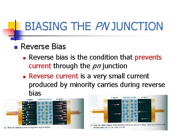
BIASING THE PN JUNCTION n Reverse Bias n n Reverse bias is the condition that prevents current through the pn junction Reverse current is a very small current produced by minority carries during reverse bias

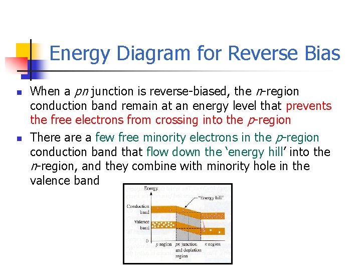
Energy Diagram for Reverse Bias n n When a pn junction is reverse-biased, the n-region conduction band remain at an energy level that prevents the free electrons from crossing into the p-region There a few free minority electrons in the p-region conduction band that flow down the ‘energy hill’ into the n-region, and they combine with minority hole in the valence band

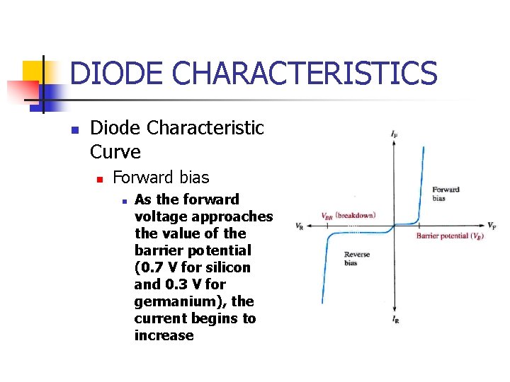
DIODE CHARACTERISTICS n Diode Characteristic Curve n Forward bias n As the forward voltage approaches the value of the barrier potential (0. 7 V for silicon and 0. 3 V for germanium), the current begins to increase

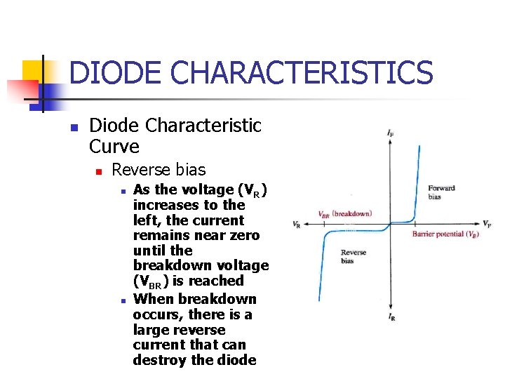
DIODE CHARACTERISTICS n Diode Characteristic Curve n Reverse bias n n As the voltage (VR) increases to the left, the current remains near zero until the breakdown voltage (VBR) is reached When breakdown occurs, there is a large reverse current that can destroy the diode

Reverse Breakdown n If the external reverse-bias voltage is increased to a large enough value, reverse breakdown occurs When one minority conduction-band electron goes toward the positive end of the pn junction, during its travel, it collides with an atom and imparts enough to knock a valence electron into the conduction band The rapid multiplication of conduction-band electrons, known as an avalanche effect