Doping and Semiconductors in Equilibrium SEMICONDUCTOR MATERIALS Semiconductors


Doping and Semiconductors in Equilibrium

SEMICONDUCTOR MATERIALS * Semiconductors are the most important class of materials that are used in solid state devices, irrespective of whether these devices are fabricated for electrical, optical, mechanical, magnetic, or (bio)chemical applications. * Semiconductor crystals can be made from both single elements and compounds. * Semiconductors that are made from single elements are called elemental semiconductors. Elemental semiconductors are found in group IV of the periodic table, e. g. , silicon, Si, and germanium, Ge. * Compound semiconductors are made up of special combinations of group III and group V elements, e. g. , gallium arsenide, Ga. As, or special combinations of group II and group VI elements, e. g. , cadmium telluride, Cd. Te. * Among the elemental semiconductors Si is by far the most commonly used semiconductor. Si is the most important material for microelectronics and integrated circuit technology. * Ga. As, on the other hand, is the most common of the compound semiconductors, and it is widely used in fabricating optical and high speed devices.

Structure and lattice properties for some known semiconductors. The lattice constants and bandgaps are given at T = 300 K.

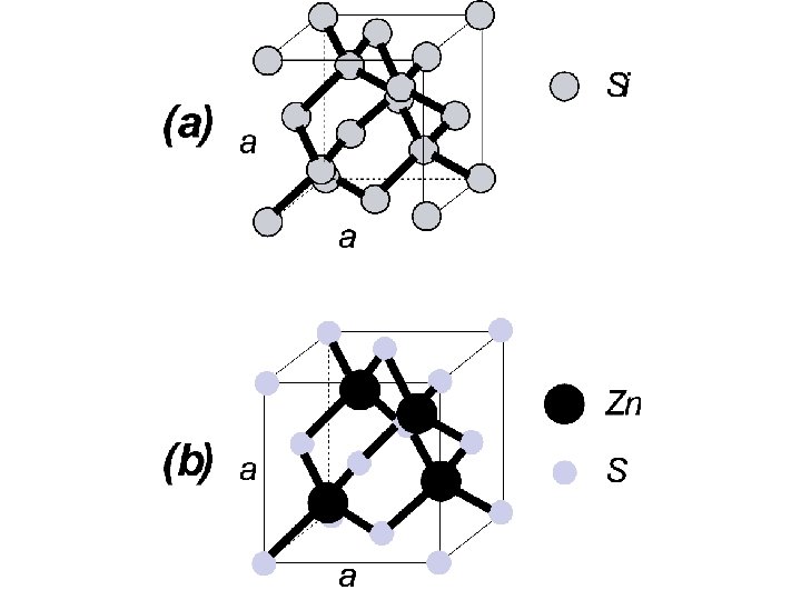
* The crystal structure of many semiconductors, including elemental semiconductors such as Si, Ge, and C and compound semiconductors such as Ga. As, Ga. P, and Zn. S, is the so-called diamond lattice. * Diamond itself could be thought of as a semiconductor with a wide band gap ~ 6 e. V and its structure is that of two interleaved face-centered cubic arrays with one array displaced a fraction of the interatomic distance from the other. * In the compound semiconductor unit cell, however, one of the two arrays is composed entirely of one atom, while the other array is composed of the other atom. This particular class of the diamond structure is called the zincblend structure. * In the diamond lattice each atom has four nearest neighbors. * In both elemental and compound semiconductors, there an average of four valence electrons per atom. Each atom is thus held in the crystal by four covalent bonds with two electrons participating in each bond.

* In a perfect semiconductor crystal and at absolute zero temperature the number of electrons available would exactly fill the inner atomic shells and the covalent bonds. * In the energy band scheme description of solids these covalent bond electrons are the electrons that fill up the valence band. * At temperatures above absolute zero some of these electrons gain enough thermal energy to break loose from these covalent bonds and make it to the conduction band. * These electrons become free electrons and are responsible for electrical conduction across the semiconductor crystal.

THE CONCEPT OF A HOLE AS A FREE CARRIER * To introduce the concept of holes in a semiconductor, we will use an elemental semiconductor, namely Si. * In a simplified two dimensional representation, each Si atom has four valence electrons in the outermost shell, and each atom shares one of these valence electrons with one of the four Si nearest neighbors; each pair of electrons constitutes a covalent bond. * Each of the two electrons in a covalent bond spends most of its time between the two nuclei. * The force of Coulombic attraction between the electrons and both nuclei holds the two atoms together.
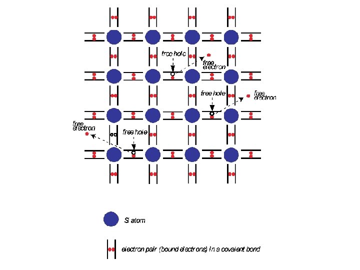

* At low temperatures the valence electrons are bound within these covalent bonds and hence restricted to move in a very limited region in proximity to the two atoms. Such electrons are called bound electrons (i. e. , bound to atoms) and are, hence, unavailable for conduction. * In terms of the energy band picture of a solid, these valence electrons in the covalent bonds are the electrons that fill up the valence band. * At higher temperatures, however, thermal vibrations may break the covalent bonds. When a bond is broken a free electron is created and can participate in current conduction. In other words a conduction electron is formed. * An "electron deficiency" is, however, left behind in the covalent bond. This electron deficiency may be corrected by an electron coming from an adjacent covalent bond, thereby moving the electron deficiency to that bond.

* This transfer of the electron deficiency from one bond to another requires the supply of no energy to the crystal lattice since all of these covalent bonds are energetically indistinguishable. * We may, therefore, regard this electron deficiency as a free particle that is able to move freely just like the free electron. This particle is called a hole. * Being a deficiency of one electron (or equivalently a deficiency of negative charge with magnitude equal to that of the charge on an electron), this hole may be regarded as carrying a positive charge of magnitude equal to that of the charge carried by an electron ; i. e. , the charge carried by a hole is +e = + 1. 6 x 10 -19 C. * In terms of the energy band scheme of solids a hole, or an electron deficiency in a covalent bond, corresponds to an empty energy state in the valence band. * Therefore holes may be thought of as positively-charged quasiparticles that populate states in the valence band.

* Observe that in our hypothetical two-dimensional Si crystal for each electron which was able to make it to the conduction band there exists a corresponding hole in the valence band ; i. e. , the net charge in the crystal is neutral. * An important consequence is, however, we are now having free charge carriers in the form of electrons in the conduction band holes in the valence band. * Due to the fact that holes are positively charged, under the influence of an electric field holes tend to move in a direction opposite to that of electrons. * Just like electrons, holes also have effective masses. To distinguish between the effective mass of an electron and the effective mass of a hole, we will hereafter use the symbol for the effective mass of the electron and the symbol for the effective mass of the hole.

INTRINSIC CARRIER CONCENTRATION * At finite temperatures, continuous thermal agitation results in the excitation of electrons from the valence band to the conduction band leaves behind holes in the valence band. * An intrinsic semiconductor is the one that contains relatively small amounts of impurities compared to thermally generated electrons and holes. * The conduction in an intrinsic semiconductor is equally shared by electrons and holes, which are supposed to be of the same concentrations. * The electron density in an incremental energy range d. E within the conduction band may be denoted by dn(E) which is the number of electrons per unit volume. * This dn(E) can be written as the product of energy states in the conduction band energy range d. E per unit volume, ge(E-Ec)d. E, and the probability of occupying these energy states f(E).

* Therefore the total concentration of electrons in the conduction band is obtained by integration over the conduction band where Etop denotes the energy at the top of the conduction band Ec is the energy at the bottom of the conduction band. Substituting for ge(E) * We will proceed by making some simplifying assumptions. First let us take our energy reference as the bottom of the conduction band Ec ; i. e. , we may set Ec = 0. Also for simplicity we assume that the energy at the top of the conduction band is very large ; i. e. , we can set Etop = ∞. Hence we may write

Which implies that the integral reduces to If we now make the substitution at E =0 we have x = 0, and at E = ∞ we have x = ∞. Also n becomes The integral is of a standard form and is equal to Therefore,

If we now go back and change our reference in energy such that the bottom of the conduction band is Ec ≠ 0, the electron density can be written as where Nc is called the effective density of states in the conduction band. At room temperature (300 K), Nc = 2. 8 x 1019 cm-3 for Si, and Nc = 4. 7 x 1017 cm-3 for Ga. As. In a very similar manner we can obtain the density of holes, p, in the valence band as where Ev is the energy at the top of the valence band, and is the effective density of states in the valence band. At room temperature, Nv=1. 04 x 1019 cm-3 for Si, and Nv = 7. 0 x 1018 cm-3 for Ga. As.

* The concentrations n and p are the equilibrium concentrations of electrons in the conduction band, and holes in the valence band, respectively ; i. e. , these are the concentrations of free electrons and free holes in the semiconductor. * These concentrations are responsible for conduction in an intrinsic material, which is a material with negligible concentration of impurities. * We also note that for an intrinsic semiconductor these concentrations n and p are equal to one another ; i. e. , we may write n = p = ni where ni is what we would call the intrinsic carrier concentration. * One may set n = p at equilibrium to get and if we substitute for Nv and Nc which gives us the position of the Fermi level in the band gap.

* Note that in both of the preceding equations we used the symbol Ei for the Fermi level EF in the intrinsic semiconductor. At room temperature the second terms in both equations are very small and * This shows that at room temperature the Fermi level of an intrinsic semiconductor lies approximately at the middle of the band gap. * Since in an intrinsic semiconductor n = p, we may use the definition of ni and write which when we substitute for n and p becomes and where Eg = Ec - Ev is the band gap. At room temperature ni is 1. 45 x 1010 cm-3 in Si, and 1. 79 x 106 cm-3 in Ga. As.
 The compound semiconductor Ga. As has an energy gap Eg = 1.")
Problem (1) The compound semiconductor Ga. As has an energy gap Eg = 1. 42 e. V, a conduction band effective density of states Nc = 4. 7 x 1017 cm-3 (at 300 K), and a valence band effective density of states Nv = 7. 0 x 1018 cm-3 (at 300 K). (i) Compute the hole concentration, p, at 300 K if the material is intrinsic. (ii) Determine the Fermi level, EF, in the gap of this intrinsic Ga. As material at 300 K. (iii) Compute the electron concentration, n, at 400 K in Ga. As if the material is still intrinsic. Solution (i) The first step here is to determine the intrinsic carrier concentration at 300 K. This is done by substituting for Nc, Nv, and Eg (1) which gives (2)
")
If the material is intrinsic, we have p = ni; i. e. , (3) (ii) The Fermi level may be determined if we take our reference point in energy as Ev, then and (4) Note that in Eq. (4) EF is the Fermi level position with respect to Ev. Substituting for Eg, Nv, and Nc at T = 300 K in Eq. (4) we get (5)
 To determine the electron concentration, n, we also need to determine ni as")
(iii) To determine the electron concentration, n, we also need to determine ni as we have done in part (i) above. However we were only given Nc and Nv at 300 K. We may, therefore, write (6) Using Eq. (6) together with the values of Nc and Nv at 300 K we get for Nc and Nv at 400 K the following values (7)
 for ni give (8) Because in an intrinsic")
which when used in Eq. (1) for ni give (8) Because in an intrinsic semiconductor n = p = ni we get for the free electron concentration, n, at 400 K (9)

EXTRINSIC CONDUCTION IN SEMICONDUCTORS : DOPED SEMICONDUCTORS N-TYPE SEMICONDUCTORS * When impurities are intentionally added to a semiconductor the semiconductor is said to be doped with impurities. * In addition to the usual band scheme in solids this doped semiconductor will have energy states associated with these impurities. * The figure shows a hypothetical two-dimensional Si crystal in which one Si atom is replaced (or substituted) by an atom from group V elements in the periodic table, namely phosphorus. * Phosphorus has five valence electrons as opposed to Si which has only four.
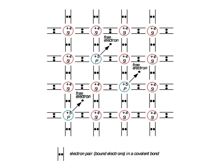

* The phosphorus atom will share four of it's electrons with four neighboring Si atoms. * The remaining fifth valence electron in phosphorus is loosely bound to the phosphorus nucleus. * Using the hydrogen atom model we can write the binding energy for electrons in the nth shell of an atom as * Except for the permittivity of free space, eo, which must be replaced by the permittivity of the semiconductor, es, and except for the free electron mass m which must be replaced by the effective mass of the electron in the semiconductor crystal, the equation above could be used to estimate the ionization energy of an impurity atom in a semiconductor crystal. If we denote this ionization energy by the symbol Ed, we can write

* When the phosphorus atom in Si is ionized, the released electron becomes a free electron which is available for conduction. In other words; this electron is donated by the phosphorus atom to the conduction band in the Si crystal. * The phosphorus atom is, hence, called a donor atom. All atoms with five valence electrons can potentially do the same thing done by phosphorus to the Si crystal ; i. e. , donate an electron to the conduction band, however the amount of energy needed, Ed, for this process to occur may differ from one type of donor atom to another. * Atoms with five valence electrons are those in group V of the periodic table. * * These atoms will donate electrons if they substitute for host atoms in crystals of group IV elemental semiconductors. * The atoms in group V of the periodic table, such as phosphorus or arsenic, are called donor atoms or simply donors and the doped semiconductor is now called extrinsic semiconductor. * When Si is doped with phosphorus the energy needed to generate a conduction electron will be ~ Ed ~ 0. 045 e. V which is very small indeed compared with the energy gap Eg. * Therefore in Si doped with phosphorus, conduction electrons are very easily generated with a supply of very little energy.

* Now imagine we are somehow able to introduce a large concentration of phosphorus atoms in an otherwise pure Si crystal, e. g. a phosphorus atom concentration of ~ 1015 cm-3. * With a minimal energy supply these phosphorus atoms will donate each an electron to the crystal amounting to a concentration of electrons in the conduction band of the order of 1015 cm-3 at room temperature. * This concentration of electrons is to be contrasted with the concentration of conduction electrons in an intrinsic Si at room temperature which is of the order of 1010 cm-3. * With this doping level a five orders of magnitude increase in the free electron concentration is achieved. Note that in a solid there are ~ 1022 - 1023 atoms/cm 3 and a doping level of ~ 1015 cm-3 is equivalent to merely replacing one Si atom in every 107 - 108 atoms/cm 3 by a phosphorus atom. * Obviously this level of doping introduces a very insignificant change in the overall crystal structure but it's effect on the free electron concentration is apparently very significant. * Notice that the conduction in this phosphorus-doped Si will be dominated by electrons.

* This can be seen by applying the relation and using the phosphorus-doped Si example discussed above. For n ~ 1015 cm-3 and ni ~ 1010 cm-3 for Si at room temperature p is of the order of 105 cm-3, which shows that the concentration of free holes is far below that of free electrons in this material. * This type of extrinsic semiconductor, or more specifically Si, is called ntype semiconductor or n-type Si. * The term n-type indicates that the charge carriers are the negativelycharged electrons. * The example discussed above was specific to Si doped with phosphorus, however, the conclusions arrived at will generally apply to all elemental semiconductors doped with atoms of a group V element ; i. e. , any elemental semiconductor doped with atoms from group V elements becomes an n-type semiconductor.

Energy diagram for doped n-type semiconductor

Common donor and acceptor atoms in Si

* After donating one of its valence electrons to the crystal the donor atom now becomes a positively charged ion ; i. e. , the donor atom is ionized. * Under the condition of complete ionization of all donor atoms, which is a reasonable assumption to make for shallow donors, we may approximate the total density of free electrons, n, in the n-type semiconductor by n = Nd, where Nd is the donor concentration. * One can write the Fermi level in terms of the effective density of states in the conduction band, Nc, and the donor concentration, Nd, as * Let us take an example of Si doped with phosphorous such that Nd ~ 1015 cm-3. The concentration of free electrons, n, in this n-type Si is n ~ 1015 cm-3 at room temperature. * We also know that for Si at room temperature Nc ~ 3 x 1019 cm-3 which implies that Ec - EF ~ 0. 3 e. V at room temperature. * This indicates that the Fermi level in this n-type material is located in the upper half of the band gap.

P-TYPE SEMICONDUCTOR * We now consider the situation where our elemental semiconductor is doped with atoms from an element in group III of the periodic table ; i. e. , atoms that have only three valence electrons. * To be more specific we will take as an example Si doped with boron as is shown in the hypothetical twodimensional Si lattice in the figure. * As it can be seen the net effect of having a boron atom substituting for Si is the creation of a free hole in the valence band.

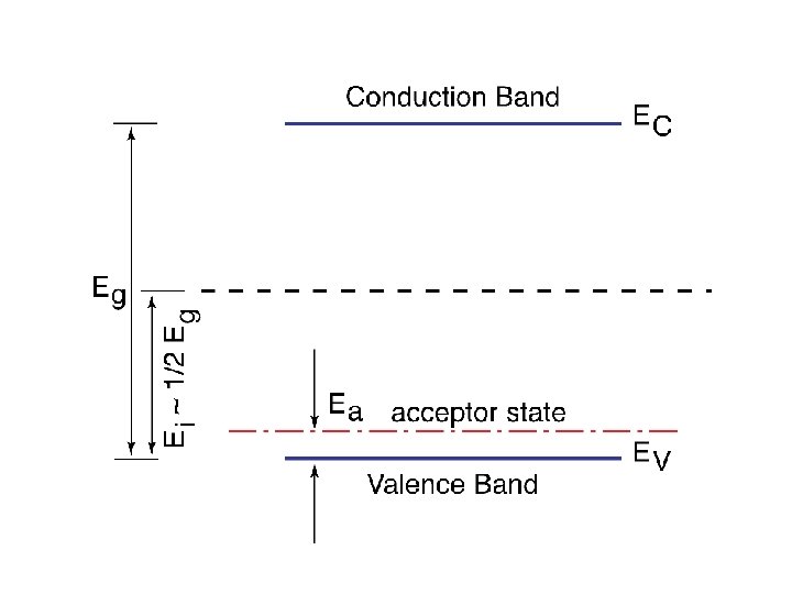
* The net effect is, hence, the generation of a free hole in the Si crystal. In terms of the energy band representation of a solid, a free hole is now generated in the valence band. * Alternatively, this process may be viewed as an electron is taken out of the valence band leaving behind a free hole. * In this case the boron atom is said to have accepted an electron from the valence band thus producing a free hole. Boron, and for that matter any atom from group III elements replacing a host atom in an elemental semiconductor crystal, is called an acceptor atom or simply acceptor. * The energy required by the electron to make a transition from the valence band to the acceptor atom, Ea, is usually very small and it specifies the position of the acceptor level in the band gap relative to the valence band edge Ev. * This is because the acceptor level communicates with the valence band electrons and, hence, the position of this level is appropriately specified with respect to Ev. * Using similar arguments as those in subsection (4. 4. 1), in Si doped with boron the conduction will be dominated by holes. Therefore this type of extrinsic semiconductor, Si in this particular example, is called p-type semiconductor or ptype Si.

Common donor and acceptor atoms in Si

* Let us assume that the concentration of acceptor atoms in the semiconductor matrix is Na. * Let us also assume that all the acceptor atoms are ionized ; i. e. , all acceptor atoms have accepted electrons from the valence band have become negatively charged. * The concentration of free holes, p, in this case is p = Na. We can obtain the corresponding Fermi level position in the energy gap as * Here again for p-type Si at room temperature with acceptor concentration Na ~ 1015 cm-3, we get EF - Ev ~ 0. 2 e. V. * This shows that in p-type Si, and at temperatures ~ 300 K, the Fermi level lies in the lower half of the band gap.
 A semiconductor of energy gap Eg = 1. 0 e. V is")
Problem (2) A semiconductor of energy gap Eg = 1. 0 e. V is doped p-type with Na = 1016 cm-3. The room temperature (300 K) effective density of states for the conduction band is Nc = 1019 cm-3, and the room temperature effective density of states for the valence band is Nv = 5. 0 x 1018 cm-3. (i) If this material were not doped, what would the intrinsic populations be at room temperature ? (ii) Calculate the band populations (n and p) at room temperature (300 K) for this p-type doped semiconductor. Solution (i) If the material were intrinsic, the intrinsic carrier concentration ni is given as (1) Substituting for Nc, Nv, and Eg at T = 300 K gives (2)
 For the p-type semiconductor, we can determine pp (the hole concentration in p-type")
(ii) For the p-type semiconductor, we can determine pp (the hole concentration in p-type material) as pp = Na = 1016 cm-3. We have for our p-type semiconductor (3) Substituting for ni and pp in Eq. (3), one gets (4)
- Slides: 38