Advances in Atomic Layer Deposition of Semiconductor Device
- Slides: 25

Advances in Atomic Layer Deposition of Semiconductor Device Manufacturing June 22, 2018 류동호(dhyou@ips. co. kr) 반도체연구소 Wonik IPS, Korea

Contents Ⅰ ALD Introduction Ⅱ ALD Applications Ⅲ Challenges of ALD V Summary 2018 진공기술 현장실무

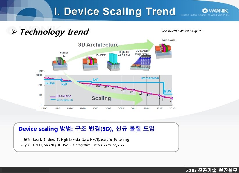
I. Device Scaling Trend Ø Technology trend ※ ASD-2017 Workshop by TEL Device scaling 방법: 구조 변경(3 D), 신규 물질 도입 - 물질 : Low-k, Strained Si, High-K/Metal Gate, HM/Spacers for Patterning - 구조 : Fin. FET, VNAND, 3 D TSV, 3 D integration, Gate-All-Around, - - - 2018 진공기술 현장실무

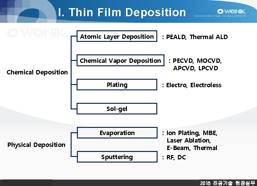
I. Thin Film Deposition Atomic Layer Deposition Chemical Vapor Deposition Chemical Deposition Plating : PEALD, Thermal ALD : PECVD, MOCVD, APCVD, LPCVD : Electro, Electroless Sol-gel Evaporation Physical Deposition Sputtering : Ion Plating, MBE, Laser Ablation, E-Beam, Thermal : RF, DC 2018 진공기술 현장실무

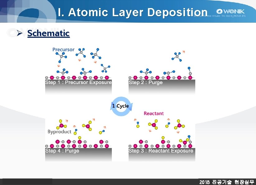
I. Atomic Layer Deposition Ø Schematic 2018 진공기술 현장실무

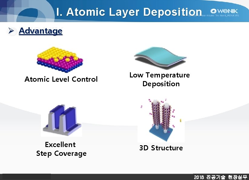
I. Atomic Layer Deposition Ø Advantage Atomic Level Control Low Temperature Deposition Excellent Step Coverage 3 D Structure 2018 진공기술 현장실무

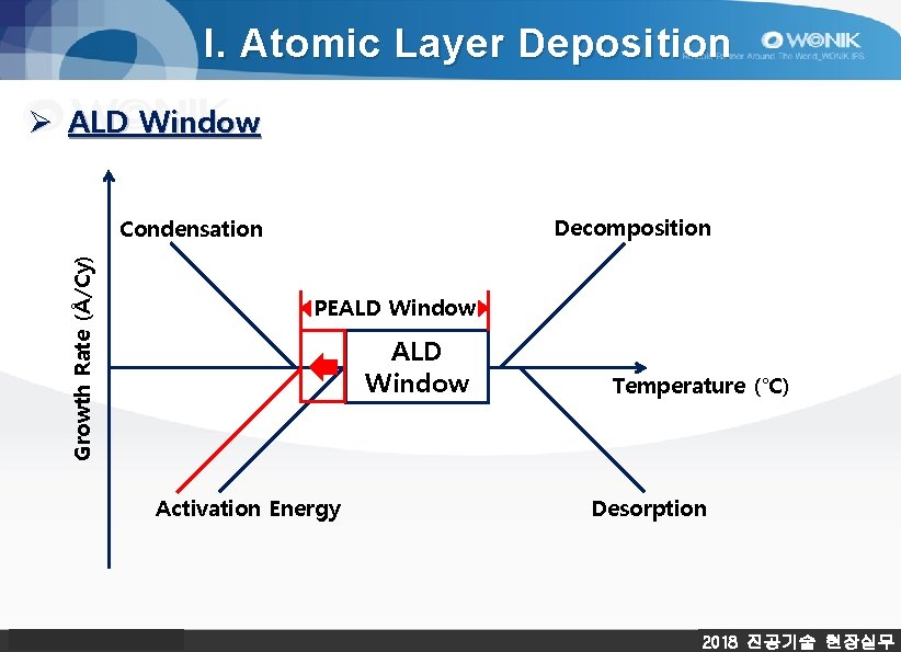
I. Atomic Layer Deposition Ø ALD Window Decomposition Growth Rate (Å/Cy) Condensation PEALD Window Activation Energy Temperature (℃) Desorption 2018 진공기술 현장실무

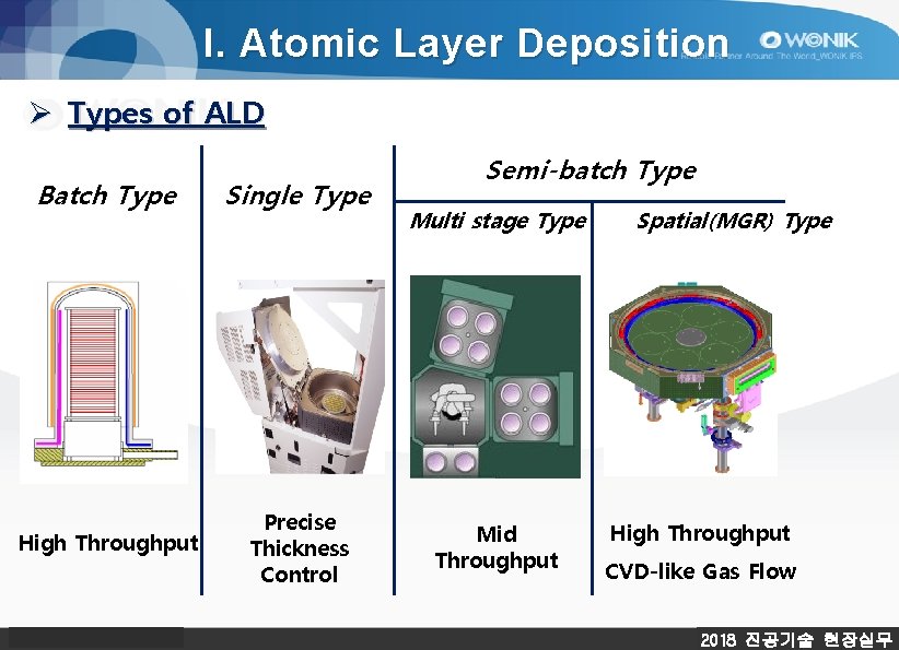
I. Atomic Layer Deposition Ø Types of ALD Batch Type Single Type High Throughput Precise Thickness Control Semi-batch Type Multi stage Type Mid Throughput Spatial(MGR) Type High Throughput CVD-like Gas Flow 2018 진공기술 현장실무

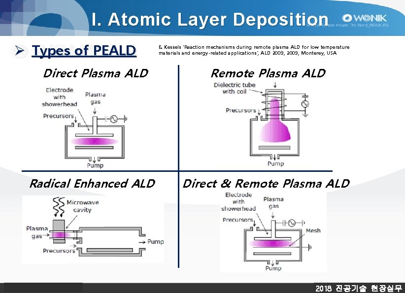
I. Atomic Layer Deposition Ø Types of PEALD E. Kessels ‘Reaction mechanisms during remote plasma ALD for low temperature materials and energy-related applications’, ALD 2009, Monterey, USA Direct Plasma ALD Remote Plasma ALD Radical Enhanced ALD Direct & Remote Plasma ALD 2018 진공기술 현장실무

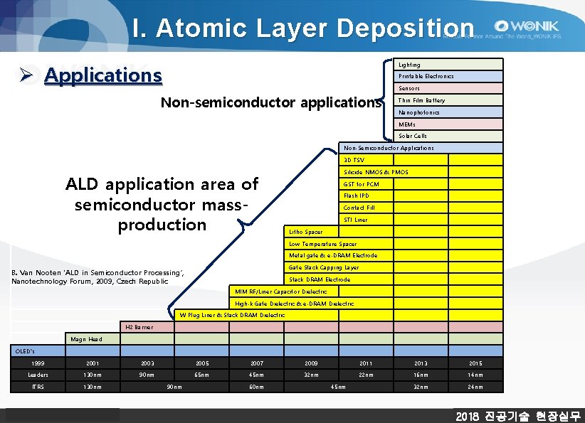
I. Atomic Layer Deposition Ø Applications Lighting Printable Electronics Sensors Non-semiconductor applications Thin Film Battery Nanophotonics MEMs Solar Cells Non-Semiconductor Applications 3 D TSV ALD application area of semiconductor massproduction Silicide NMOS & PMOS GST for PCM Flash IPD Contact Fill STI Liner Litho Spacer Low Temperature Spacer Metal gate & e-DRAM Electrode Gate Stack Capping Layer B. Van Nooten ‘ALD in Semiconductor Processing’, Nanotechnology Forum, 2009, Czech Republic Stack DRAM Electrode MIM RF/Liner Capacitor Dielectric High-k Gate Dielectric & e-DRAM Dielectric W Plug Liner & Stack DRAM Dielectric H 2 Barrier Magn Head OLED`s 1999 2001 2003 2005 2007 2009 2011 2013 2015 Leaders 130 nm 90 nm 65 nm 45 nm 32 nm 22 nm 16 nm 14 nm ITRS 130 nm 32 nm 24 nm 90 nm 60 nm 45 nm 2018 진공기술 현장실무

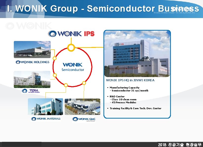
I. WONIK Group - Semiconductor Business WONIK IPS HQ in JINWI KOREA § Manufacturing Capacity - Semiconductor 31 sys/month § R&D Center - Class 10 clean room - 45 Process Modules § Training Facility & Core Tech. Dev. Center 2018 진공기술 현장실무

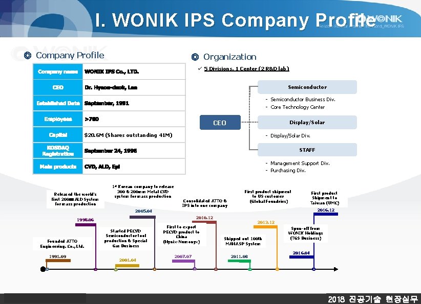
I. WONIK IPS Company Profile ◎ Organization ü 5 Divisions, 1 Center (2 R&D lab) Semiconductor - Semiconductor Business Div. - Core Technology Center Employees CEO Display/Solar $20. 6 M (Shares outstanding 41 M) Capital - Display/Solar Div. KOSDAQ Registration STAFF - Management Support Div. - Purchasing Div. Released the world's first 200㎜ ALD System for mass production 1 st Korean company to release 300 & 200 mm Metal CVD system for mass production Consolidated ATTO & IPS into one company First product shipment to US customer (Global Foundries) First product Shipment to Taiwan (UMC) 2016. 12 2005. 04 2010. 12 1998. 06 Founded ATTO Engineering. Co. , Ltd. 1991. 09 Started PECVD Semiconductor tool production & Special Gas Business 2001. 04 First to export PECVD product to China (Hynix-Numonyx) 2007. 07 2013. 12 Shipped out 100 th MAHA SP System 2011. 08 Spun-off from WONIK Holdings (TGS Business) 2016. 04 2018 진공기술 현장실무

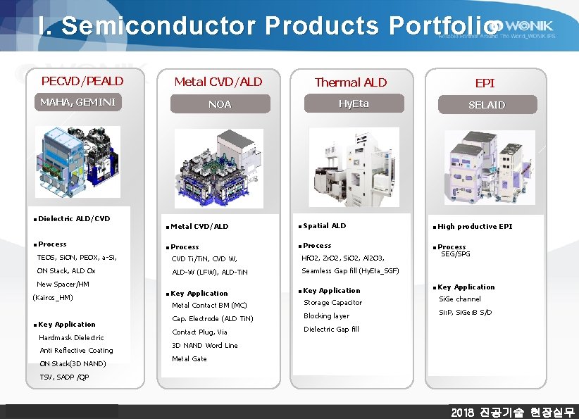
I. Semiconductor Products Portfolio PECVD/PEALD Metal CVD/ALD MAHA, GEMINI ■ Dielectric ALD/CVD ■ Process Thermal ALD Hy. Eta NOA ■ Spatial ALD ■ High productive EPI ■ Process CVD Ti/Ti. N, CVD W, Hf. O 2, Zr. O 2, Si. O 2, Al 2 O 3, ON Stack, ALD Ox ALD-W (LFW), ALD-Ti. N Seamless Gap fill (Hy. Eta_SGF) New Spacer/HM ■ Key Application Hardmask Dielectric Anti Reflective Coating ON Stack(3 D NAND) SELAID ■ Metal CVD/ALD TEOS, Si. ON, PEOX, a-Si, (Kairos_HM) EPI ■ Key Application SEG/SPG ■ Key Application Metal Contact BM (MC) Storage Capacitor Si. Ge channel Cap. Electrode (ALD Ti. N) Blocking layer Si: P, Si. Ge: B S/D Contact Plug, Via Dielectric Gap fill 3 D NAND Word Line Metal Gate TSV, SADP /QP 2018 진공기술 현장실무

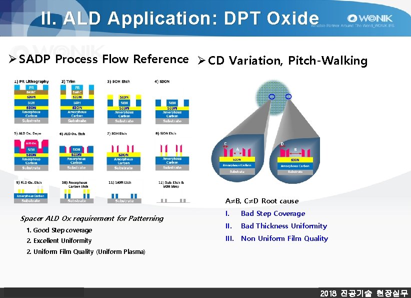
II. ALD Application: DPT Oxide Ø SADP Process Flow Reference Ø CD Variation, Pitch-Walking A≠B, C≠D Root cause Spacer ALD Ox requirement for Patterning 1. Good Step coverage 2. Excellent Uniformity I. Bad Step Coverage II. Bad Thickness Uniformity III. Non Uniform Film Quality 2. Uniform Film Quality (Uniform Plasma) 2018 진공기술 현장실무

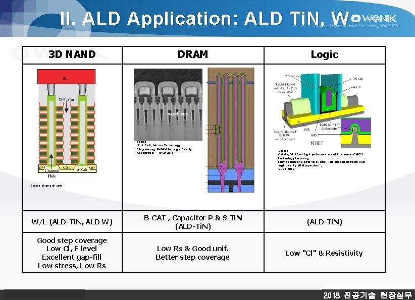
II. ALD Application : ALD Ti. N, W 3 D NAND DRAM Source : Kirk Prall, Micron Technology, “Engineering Re. RAM for High-Density Applications “, IDEM 2014 Logic Source : C. Auth, “A 22 nm high performance and low-power CMOS technology featuring fully-depleted tri-gate transistors, self-aligned contacts and high density MIM capacitors”, VLSIT 2012 Source : chipworks. com W/L (ALD-Ti. N, ALD W) B-CAT , Capacitor P & S-Ti. N (ALD-Ti. N) Good step coverage Low Cl, F level Excellent gap-fill Low stress, Low Rs & Good unif. Better step coverage Low “Cl” & Resistivity 2018 진공기술 현장실무

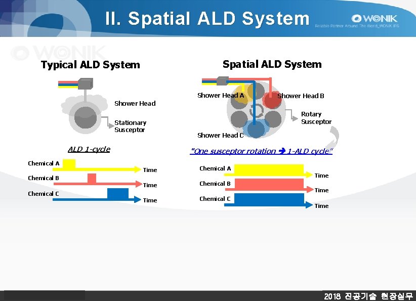
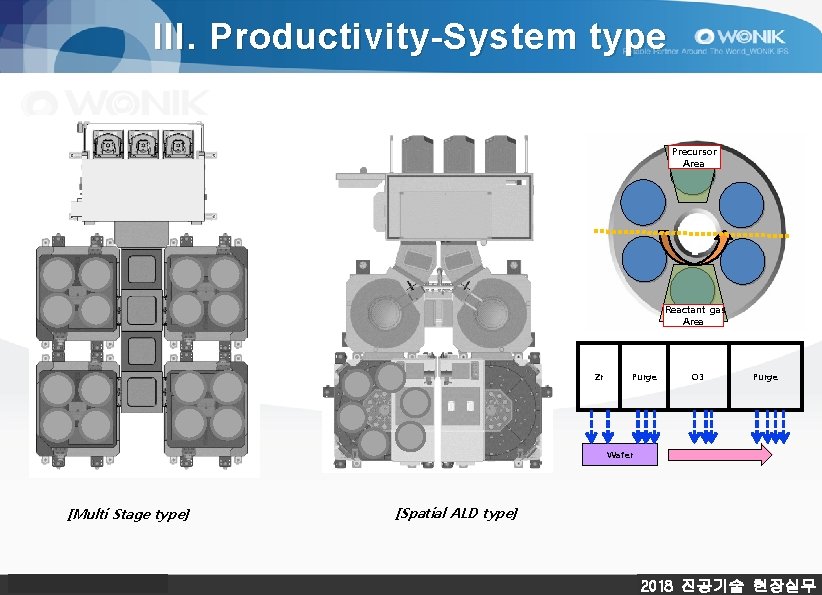
II. Spatial ALD System Typical ALD System Shower Head A Shower Head B Shower Head Stationary Susceptor ALD 1 -cycle Rotary Susceptor Shower Head C “One susceptor rotation 1 -ALD cycle” Chemical A Time Chemical B Time Chemical C Chemical B Chemical C Time 2018 진공기술 현장실무

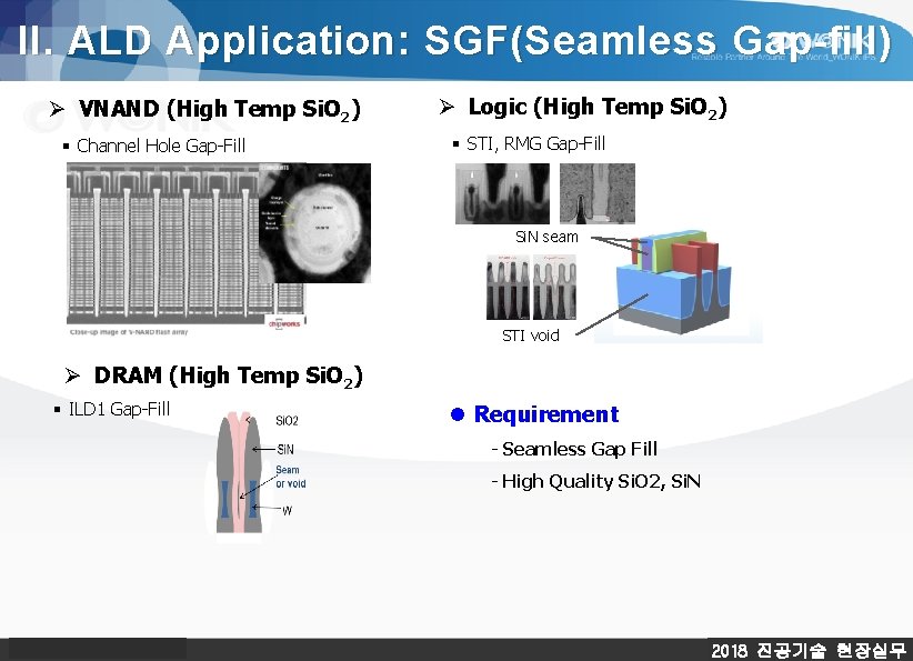
II. ALD Application: SGF(Seamless Gap-fill) Ø VNAND (High Temp Si. O 2) § Channel Hole Gap-Fill Ø Logic (High Temp Si. O 2) § STI, RMG Gap-Fill Si. N seam STI void Ø DRAM (High Temp Si. O 2) § ILD 1 Gap-Fill l Requirement - Seamless Gap Fill - High Quality Si. O 2, Si. N 2018 진공기술 현장실무

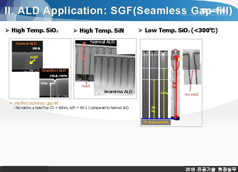
II. ALD Application: SGF(Seamless Gap-fill) Ø High Temp. Si. O 2 Ø High Temp. Si. N Ø Low Temp. Si. O 2 (<300℃) Normal ALD 300Å void Seamless ALD 150Å=50% 95% 94 % void Seamless ALD 74% No void § Verified seamless gap-fill : No void in a hole(Top CD = 60 nm, A/R = 40: 1 ) compared to Normal ALD 56 % ‘V’ shape growth 2018 진공기술 현장실무

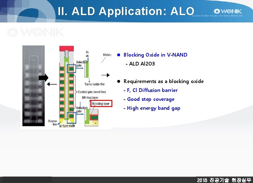
II. ALD Application: ALO l Blocking Oxide in V-NAND - ALD Al 2 O 3 l Requirements as a blocking oxide - F, Cl Diffusion barrier - Good step coverage - High energy band gap 2018 진공기술 현장실무

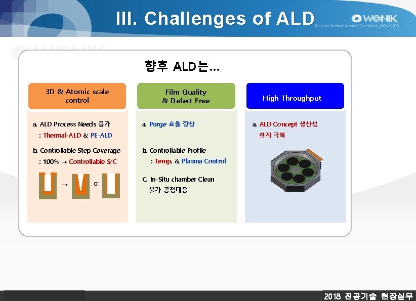
III. Challenges of ALD 향후 ALD는… 3 D & Atomic scale control a. ALD Process Needs 증가 Film Quality & Defect Free a. Purge 효율 향상 : Thermal-ALD & PE-ALD b. Controllable Step-Coverage : 100% → Controllable S/C → or High Throughput a. ALD Concept 생산성 한계 극복 b. Controllable Profile : Temp. & Plasma Control C. In-Situ chamber Clean 불가 공정대응 2018 진공기술 현장실무

III. Productivity-System type Precursor Area Reactant gas Area Zr Purge O 3 Purge Wafer [Multi Stage type] [Spatial ALD type] 2018 진공기술 현장실무

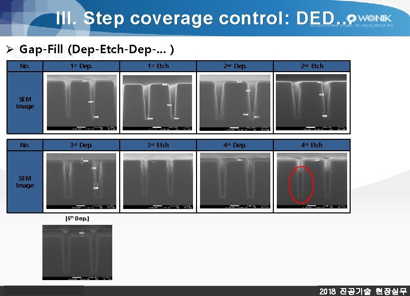
III. Step coverage control: DED… Ø Gap-Fill (Dep-Etch-Dep-. . . ) No. 1 st Dep. 1 st Etch 2 nd Dep. 2 nd Etch 3 rd Dep. 3 rd Etch 4 th Dep. 4 th Etch SEM Image No. SEM Image [5 th Dep. ] 2018 진공기술 현장실무

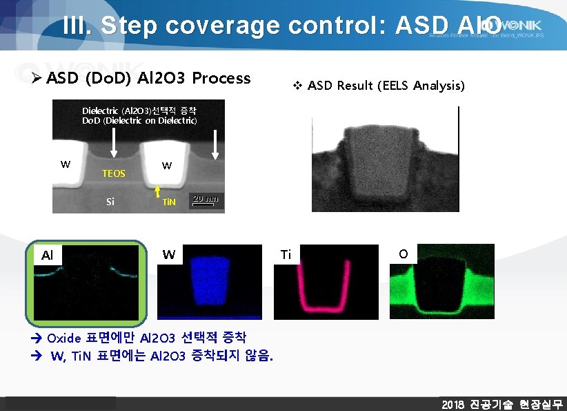
III. Step coverage control: ASD Al. O Ø ASD (Do. D) Al 2 O 3 Process v ASD Result (EELS Analysis) Dielectric (Al 2 O 3)선택적 증착 Do. D (Dielectric on Dielectric) W TEOS Si Al W Ti. N W Ti O Oxide 표면에만 Al 2 O 3 선택적 증착 W, Ti. N 표면에는 Al 2 O 3 증착되지 않음. 2018 진공기술 현장실무

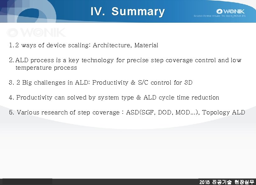
IV. Summary 1. 2 ways of device scaling: Architecture, Material 2. ALD process is a key technology for precise step coverage control and low temperature process 3. 2 Big challenges in ALD: Productivity & S/C control for 3 D 4. Productivity can solved by system type & ALD cycle time reduction 5. Various research of step coverage : ASD(SGF, DOD, MOD. . . ), Topology ALD 2018 진공기술 현장실무

감사합니다. Copyright (c) 2013 Wonik IPS Co. , Ltd. All rights reserved. 2018 진공기술 현장실무