Week 10 a Introduction to Semiconductors and Diodes


")
 + VD –")
 + C R + v.")


 but the")
 works, look first at the voltage polarity")


 • An electric field is applied normal to the")
 Crystals are grown from a melt in boules (cylinders) with specified")

 or “dry” oxidation “wet” oxidation •")

 process step photoresist")


- Slides: 31
Week 10 a – Introduction to Semiconductors and Diodes What’s different about semiconductors? What are “holes” in a semiconductor? What’s a p-type and what’s an n-type semiconductor? What’s a pn diode and what is its I-V characteristic? How can I use diodes? How can I convert 120 -volt AC to a few volts DC for my end-of-term music system project? How are semiconductor devices such as diodes, fieldeffect transistors and integrated circuits made?
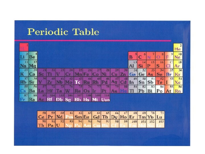
What is a Semiconductor? • Low resistivity => “conductor” • High resistivity => “insulator” • Intermediate resistivity => “semiconductor” – Generally, the semiconductor material used in integrated-circuit devices is crystalline • In recent years, however, non-crystalline semiconductors have become commercially very important polycrystalline amorphous crystalline
Semiconductor Materials Elemental: Compound:
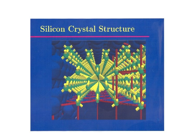
Electronic Properties of Si Silicon is a semiconductor material. Pure Si has relatively high resistivity at room temperature. There are 2 types of mobile charge-carriers in Si: Conduction electrons are negatively charged. Holes are positively charged. They are an “absence of electrons”. The concentration of conduction electrons & holes in a semiconductor can be affected in several ways: 1. 2. by changing the temperature by adding special impurity atoms (dopants) 3. 4. by applying a high electric field by irradiation with high-energy particles
Conduction Electrons and Holes 2 -D representation When an electron breaks loose and becomes a conduction electron, a hole is also created. Si Si Si Note: A hole (along with its associated positive charge) is mobile!
Definition of Parameters n = number of mobile electrons per cm 3 p = number of holes per cm 3 ni = intrinsic carrier concentration (#/cm 3) In a pure semiconductor, n = p = ni
The pn Junction Diode Schematic diagram p-type Circuit symbol ID n-type net acceptor concentration NA net donor concentration ND cross-sectional area AD Physical structure: (an example) For simplicity, assume that the doping profile changes abruptly at the junction. + ID + VD metal Si. O 2 VD Si. O 2 p-type Si n-type Si – – metal
Water Model of Diode Rectifier Simplistic view of why a pn-diode conducts differently in forward and reverse bias: When the p side is made positive with respect to the n side (forward bias), the positively charged holes move toward the negatively charged electrons, and they recombine. Then more carriers flow in from the contacts. In reverse bias, the holes and the S electrons move away from each other, leaving no mobile carriers in the middle – hence, the diode has an insulator in its i middle region and no current flows through. m p l i
Summary: pn-Junction Diode I-V • Under forward bias, current increases exponentially with increasing forward bias • Under reverse bias, a potential barrier in the middle of the junction is increased, so that negligible carriers flow across the junction ID (A) The net result is an I-V curve that looks like this, with typically n. A currents in the reverse direction (VD < 0), and m. A or more in the forward direction (VD > 0) | 0. 7 V for Si VD (V)
Ideal Diode Model of pn Diode Circuit symbol ID + I-V characteristic ID (A) VD – Switch model ID forward bias reverse bias VD (V) • An ideal diode passes current only in one direction. • An ideal diode has the following properties: • when ID > 0, VD = 0 • when VD < 0, ID = 0 Diode behaves like a switch: • closed in forward bias mode • open in reverse bias + VD –
Large-Signal Diode Model Circuit symbol ID + I-V characteristic ID (A) + VD – Switch model ID + Vturn-on forward bias reverse bias Vturn-on VD (V) VD – For a Si pn diode, Vturn-on 0. 7 V RULE 1: When ID > 0, VD = Vturn-on RULE 2: When VD < Vturn-on, ID = 0 Diode behaves like a voltage source in series with a switch: • closed in forward bias mode • open in reverse bias
Application Example: Rectification using the ideal diode model vs(t) + C R + v. R(t) – vs(t) t v. R(t) t
Converting AC to DC Using a “full-wave” diode rectifier circuit (used in the music system end-of-term project) The 20: 1 turns ratio transformer here reduces the rms voltage from the wall outlet (120 V) by a factor of 20 to 6 volts rms. The voltage across the load resistor still has positive and negative values.
Putting a single diode in the circuit eliminates the negativegoing voltages, but is inefficient because of that, and the output voltage is not a steady value as a function of time.
Using four diodes connected as shown produces only positive-going voltages (more efficient) but the voltage is not steady – it has very large “ripple”.
To see how the four-diode (full-wave rectifier) works, look first at the voltage polarity across the load resistor. When the top of the transformer secondary is positive, the two diodes shown are forward biased and the current is downward through the load resistor. When the top of the transformer is negative with respect to the bottom, these two diodes are reverse-biased and pass no current.
When the top terminal of the transformer is negative, the other two diodes are forward-biased and pass current through the load resistor from top to bottom, filling in the missing parts of the output waveform.
The output can be filtered by adding a capacitor across the load resistor, reducing the ripple significantly. The time constant RLC needs to be large compared with the period of the AC part of the output waveform. What is the frequency of that AC part? And what is its period?
To get a really steady voltage out we can add an integrated circuit regulator to the circuit.
A Bit About Semiconductor Device Fabrication How are semiconductor devices such as diodes, fieldeffect transistors and integrated circuits made?
Modern Field Effect Transistor (FET) • An electric field is applied normal to the surface of the semiconductor (by applying a voltage to an overlying “gate” electrode), to modulate the conductance of the semiconductor ® Modulate drift current flowing between 2 contacts (“source” and “drain”) by varying the voltage on the “gate” electrode Metal-oxide-semiconductor (MOS) FET:
Si Substrates (Wafers) Crystals are grown from a melt in boules (cylinders) with specified dopant concentrations. They are ground perfectly round and oriented (a “flat” or “notch” is ground along the boule) and then sliced like baloney into wafers. The wafers are then polished. 300 mm Typical wafer cost: $50 Sizes: 150 mm, 200 mm, 300 mm diameter “notch” indicates crystal orientation
The goal is to allow dopant atoms to diffuse into well-defined regions of the wafer to make p-type and n-type semiconductors there. Silicon dioxide is grown on the silicon wafer and then suitable holes are etched through the oxide to let dopant atoms enter and make p- or n-type silicon Silicon wafer, 100 m thick Thermal oxidation grows Si. O 2 on Si, but it consumes Si, so the wafer gets thinner. Suppose we grow 1 m of oxide: 101 m 99 m thick Si, with 1 m Si. O 2 all around total thickness = 101 m
Thermal Oxidation of Silicon (like rust on iron) or “dry” oxidation “wet” oxidation • Temperature range: § 700 o. C to 1100 o. C • Process: § O 2 or H 2 O diffuses through Si. O 2 and reacts with Si at the interface to form more Si. O 2 • 1 m of Si. O 2 formed consumes ~0. 5 m of Si oxide thickness time, t
Patterning the Layers Planar processing consists of a sequence of additive and subtractive steps with lateral patterning oxidation deposition implantation etching lithography Lithography refers to the process of transferring a pattern to the surface of the wafer Equipment, materials, and processes needed: • A mask (for each layer to be patterned) with the desired pattern • A light-sensitive material (called photoresist) covering the wafer so as to receive the pattern • A light source and method of projecting the image of the mask onto the photoresist (“printer” or “projection stepper” or “projection scanner”) • A method of “developing” the photoresist, that is selectively removing it from the regions where it was exposed
The Photo-Lithographic Process optical mask oxidation photoresist exposure photoresist removal (ashing) process step photoresist coating spin, rinse, dry acid etch photoresist develop
Photoresist Exposure • A glass mask with a black/clear pattern is used to expose a wafer coated with ~1 m thick photoresist UV light Mask Lens Image of mask appears here (3 dark areas, 4 light areas) photoresist Si wafer Mask image is demagnified by n. X “ 10 X stepper” “ 4 X stepper” “ 1 X stepper” Areas exposed to UV light are susceptible to chemical removal
The resist is exposed in the ranges 0 < x < 2 m & 3 < x < 5 m: 0 1 2 3 4 5 x [ m] mask pattern resist 0 1 2 3 4 5 x [ m] The resist will dissolve in high p. H solutions wherever it was exposed: resist after development 0 1 2 3 4 5 x [ m]
IC Fabrication – the final steps 1. After apertures have been chemically or plasma etched in the protective Si. O 2 coating, the wafer can be put in a heated chemical-vapor-deposition (CVD) chamber where dopant atoms diffuse into the silicon, making defined regions either p-type or n-type. 2. These steps are repeated many times with different optical masks and dopants, eventually forming diodes, field-effect transistors, resistors and capacitors. 3. Finally conductive coatings of aluminum or other materials are deposited and patterned to connect up the devices that were formed. 4. Then the wafer is cut with a diamond saw into “die” measuring from a few mm 2 to a cm 2 in area. The die are then put into packages, fine wires are attached, and the devices are ready for test and use.