Different Electronic Materials Semiconductors Elemental Si Ge Compound

- Slides: 35

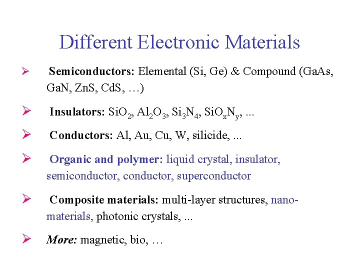
Different Electronic Materials Ø Semiconductors: Elemental (Si, Ge) & Compound (Ga. As, Ga. N, Zn. S, Cd. S, …) Ø Insulators: Si. O 2, Al 2 O 3, Si 3 N 4, Si. Ox. Ny, . . . Ø Conductors: Al, Au, Cu, W, silicide, . . . Ø Organic and polymer: liquid crystal, insulator, semiconductor, superconductor Ø Composite materials: multi-layer structures, nanomaterials, photonic crystals, . . . Ø More: magnetic, bio, …

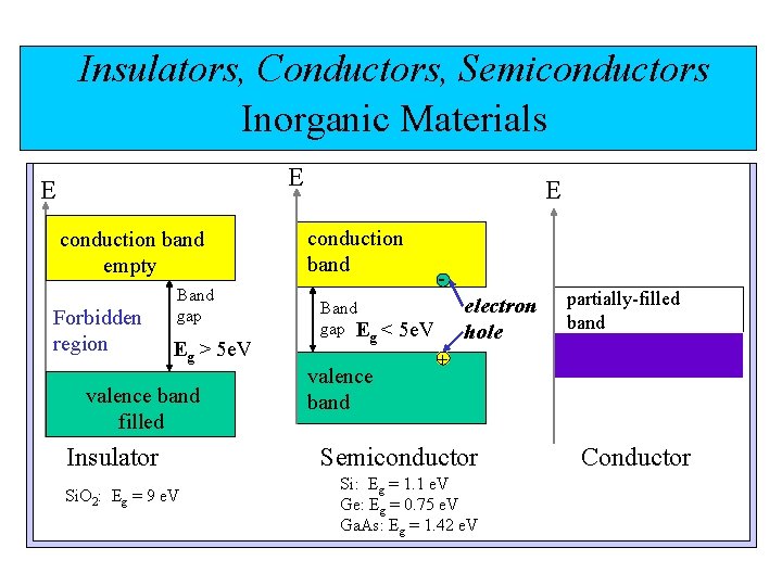
Insulators, Conductors, Semiconductors Inorganic Materials E E conduction band empty Forbidden region Band gap Eg > 5 e. V valence band filled Insulator Si. O 2: Eg = 9 e. V E conduction band Band gap Eg < valence band electron hole 5 e. V partially-filled band + Semiconductor Si: Eg = 1. 1 e. V Ge: Eg = 0. 75 e. V Ga. As: Eg = 1. 42 e. V Conductor

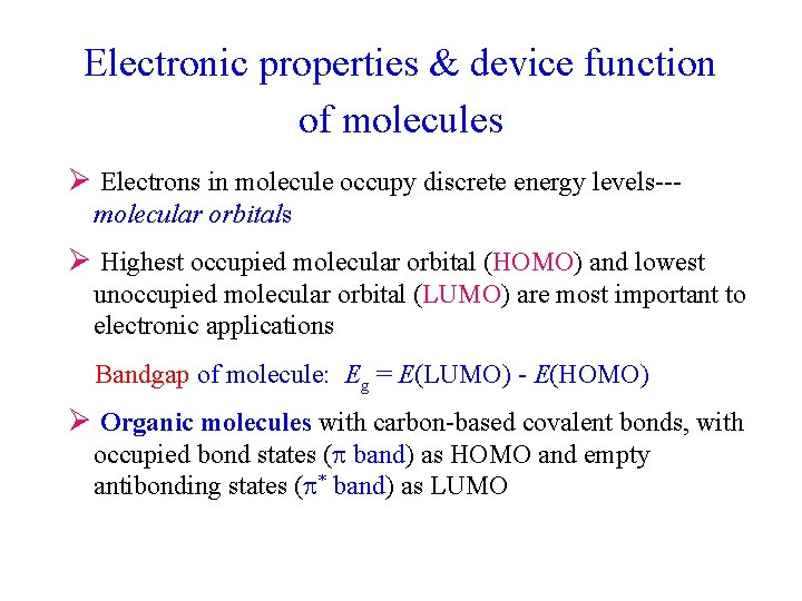
Electronic properties & device function of molecules Ø Electrons in molecule occupy discrete energy levels--molecular orbitals Ø Highest occupied molecular orbital (HOMO) and lowest unoccupied molecular orbital (LUMO) are most important to electronic applications Bandgap of molecule: Eg = E(LUMO) - E(HOMO) Ø Organic molecules with carbon-based covalent bonds, with occupied bond states ( band) as HOMO and empty antibonding states ( * band) as LUMO

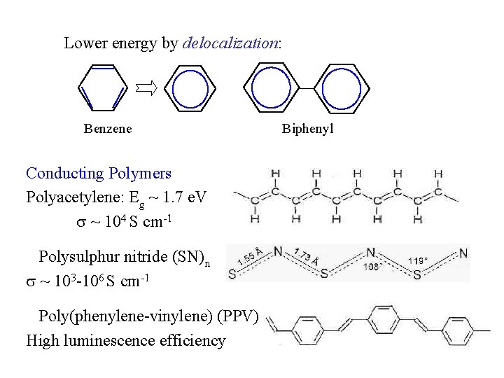
Lower energy by delocalization: Benzene Conducting Polymers Polyacetylene: Eg ~ 1. 7 e. V ~ 104 S cm-1 Polysulphur nitride (SN)n ~ 103 -106 S cm-1 Poly(phenylene-vinylene) (PPV) High luminescence efficiency Biphenyl

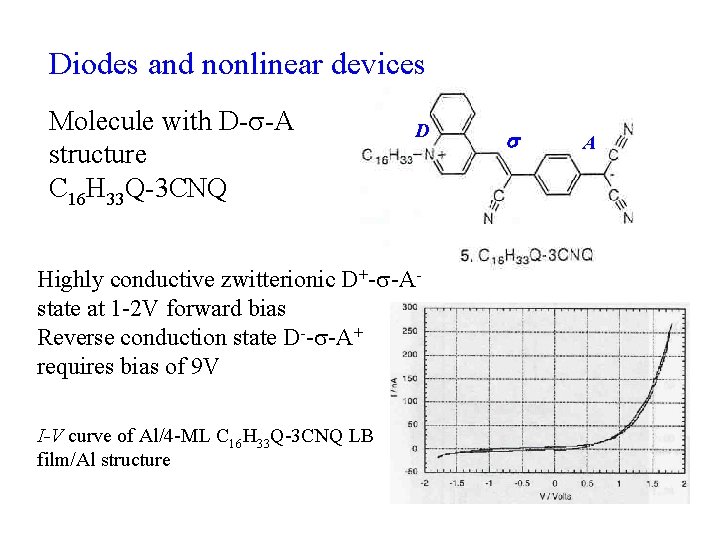
Diodes and nonlinear devices Molecule with D- -A structure C 16 H 33 Q-3 CNQ D Highly conductive zwitterionic D+- -A- state at 1 -2 V forward bias Reverse conduction state D-- -A+ requires bias of 9 V I-V curve of Al/4 -ML C 16 H 33 Q-3 CNQ LB film/Al structure A

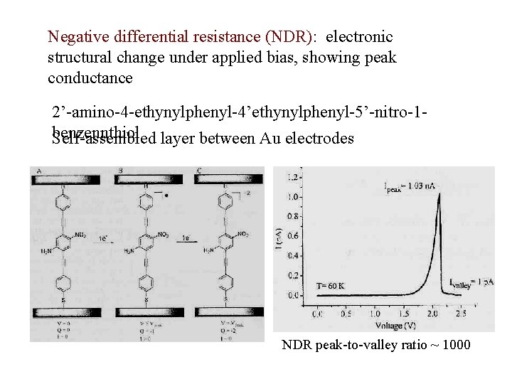
Negative differential resistance (NDR): electronic structural change under applied bias, showing peak conductance 2’-amino-4 -ethynylphenyl-4’ethynylphenyl-5’-nitro-1 benzennthiol Self-assembled layer between Au electrodes NDR peak-to-valley ratio ~ 1000

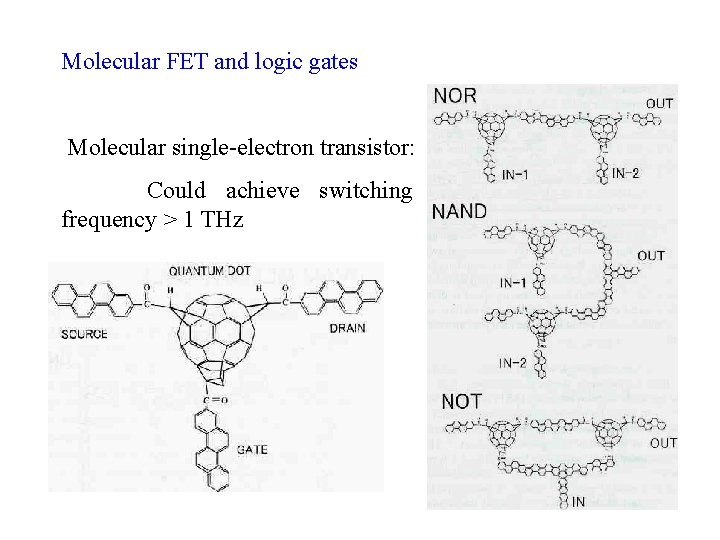
Molecular FET and logic gates Molecular single-electron transistor: Could achieve switching frequency > 1 THz

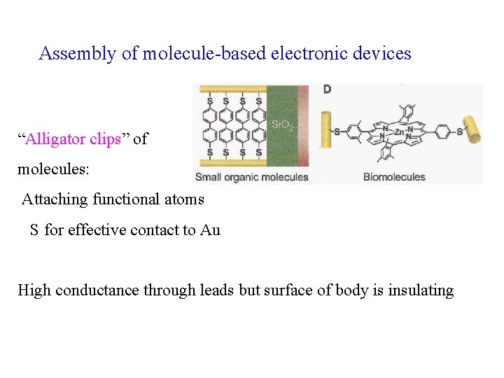
Assembly of molecule-based electronic devices “Alligator clips” of molecules: Attaching functional atoms S for effective contact to Au High conductance through leads but surface of body is insulating

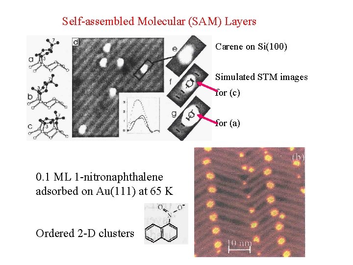
Self-assembled Molecular (SAM) Layers Carene on Si(100) Simulated STM images for (c) for (a) 0. 1 ML 1 -nitronaphthalene adsorbed on Au(111) at 65 K Ordered 2 -D clusters

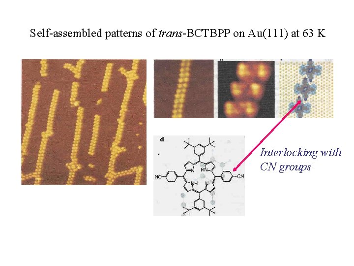
Self-assembled patterns of trans-BCTBPP on Au(111) at 63 K Interlocking with CN groups

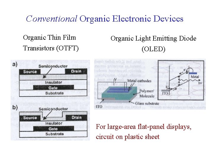
Conventional Organic Electronic Devices Organic Thin Film Organic Light Emitting Diode Transistors (OTFT) (OLED) For large-area flat-panel displays, circuit on plastic sheet

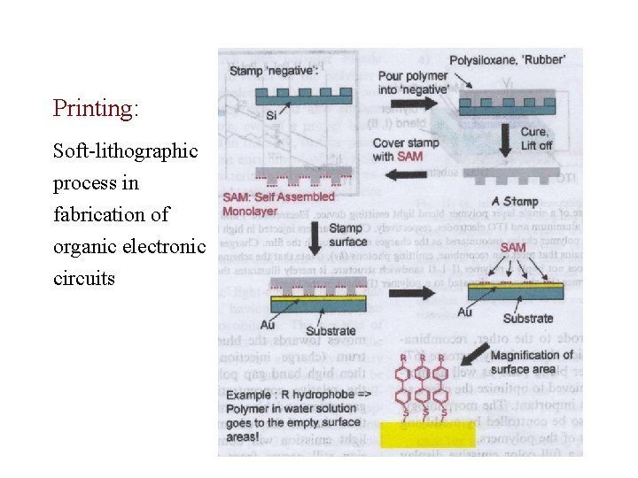
Printing: Soft-lithographic process in fabrication of organic electronic circuits

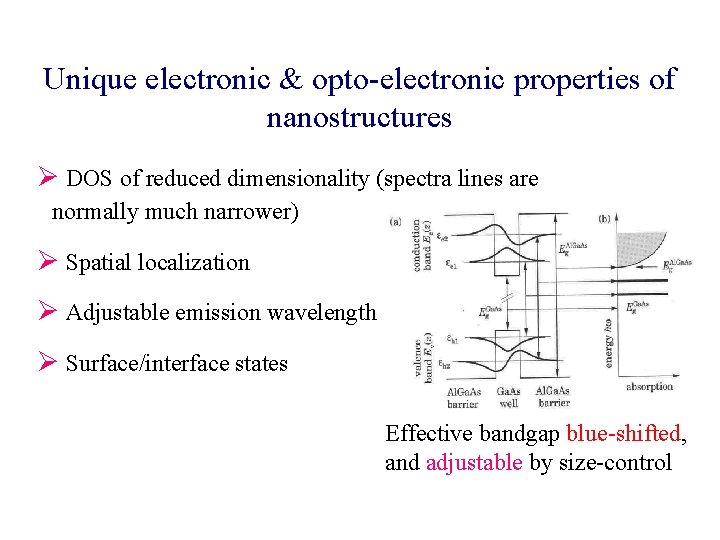
Unique electronic & opto-electronic properties of nanostructures Ø DOS of reduced dimensionality (spectra lines are normally much narrower) Ø Spatial localization Ø Adjustable emission wavelength Ø Surface/interface states Effective bandgap blue-shifted, and adjustable by size-control

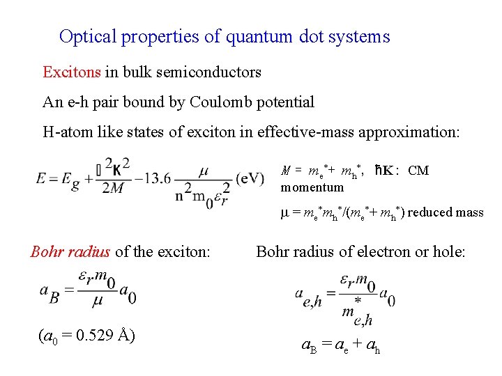
Optical properties of quantum dot systems Excitons in bulk semiconductors An e-h pair bound by Coulomb potential H-atom like states of exciton in effective-mass approximation: M = me*+ mh*, ħK: CM momentum = me*mh*/(me*+ mh*) reduced mass Bohr radius of the exciton: (a 0 = 0. 529 Å) Bohr radius of electron or hole: a. B = ae + ah

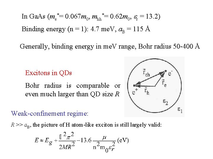
In Ga. As (me*= 0. 067 m 0, mhh*= 0. 62 m 0, r = 13. 2) Binding energy (n = 1): 4. 7 me. V, a. B = 115 Å Generally, binding energy in me. V range, Bohr radius 50 -400 Å Excitons in QDs Bohr radius is comparable or even much larger than QD size R Weak-confinement regime: R >> a. B, the picture of H atom-like exciton is still largely valid:

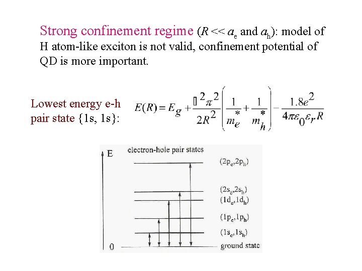
Strong confinement regime (R << ae and ah): model of H atom-like exciton is not valid, confinement potential of QD is more important. Lowest energy e-h pair state {1 s, 1 s}:

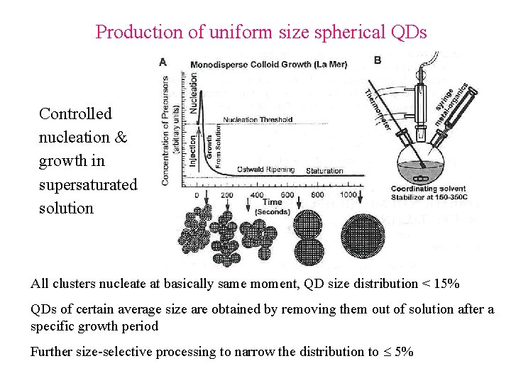
Production of uniform size spherical QDs Controlled nucleation & growth in supersaturated solution All clusters nucleate at basically same moment, QD size distribution < 15% QDs of certain average size are obtained by removing them out of solution after a specific growth period Further size-selective processing to narrow the distribution to 5%

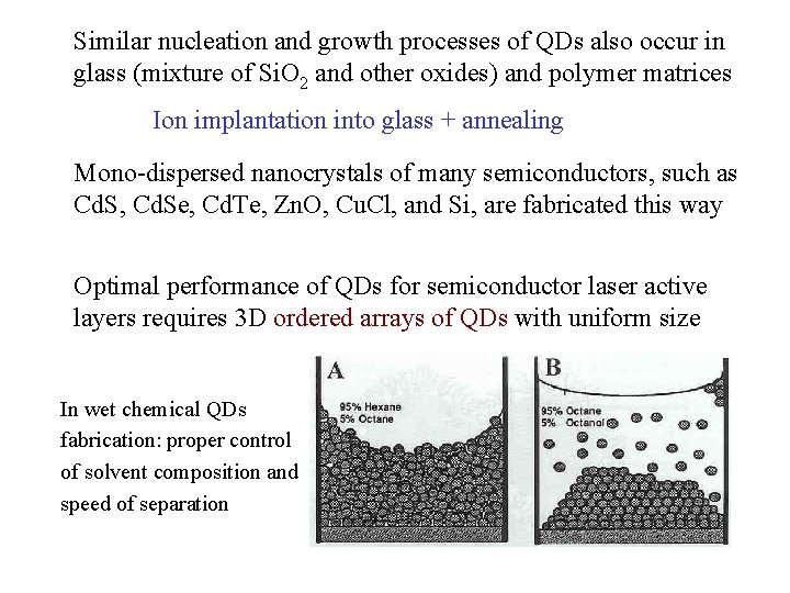
Similar nucleation and growth processes of QDs also occur in glass (mixture of Si. O 2 and other oxides) and polymer matrices Ion implantation into glass + annealing Mono-dispersed nanocrystals of many semiconductors, such as Cd. S, Cd. Se, Cd. Te, Zn. O, Cu. Cl, and Si, are fabricated this way Optimal performance of QDs for semiconductor laser active layers requires 3 D ordered arrays of QDs with uniform size In wet chemical QDs fabrication: proper control of solvent composition and speed of separation

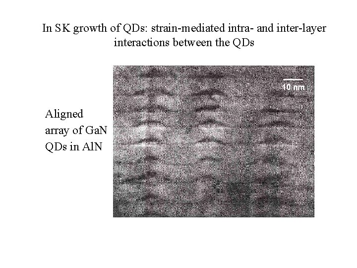
In SK growth of QDs: strain-mediated intra- and inter-layer interactions between the QDs Aligned array of Ga. N QDs in Al. N

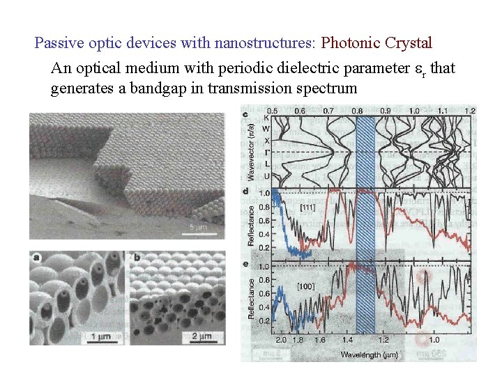
Passive optic devices with nanostructures: Photonic Crystal An optical medium with periodic dielectric parameter r that generates a bandgap in transmission spectrum

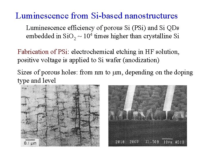
Luminescence from Si-based nanostructures Luminescence efficiency of porous Si (PSi) and Si QDs embedded in Si. O 2 ~ 104 times higher than crystalline Si Fabrication of PSi: electrochemical etching in HF solution, positive voltage is applied to Si wafer (anodization) Sizes of porous holes: from nm to m, depending on the doping type and level

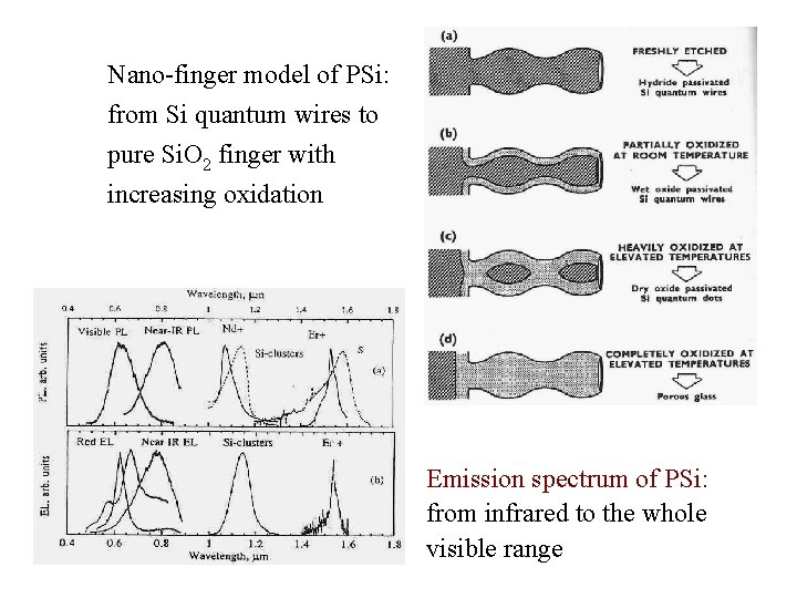
Nano-finger model of PSi: from Si quantum wires to pure Si. O 2 finger with increasing oxidation Emission spectrum of PSi: from infrared to the whole visible range

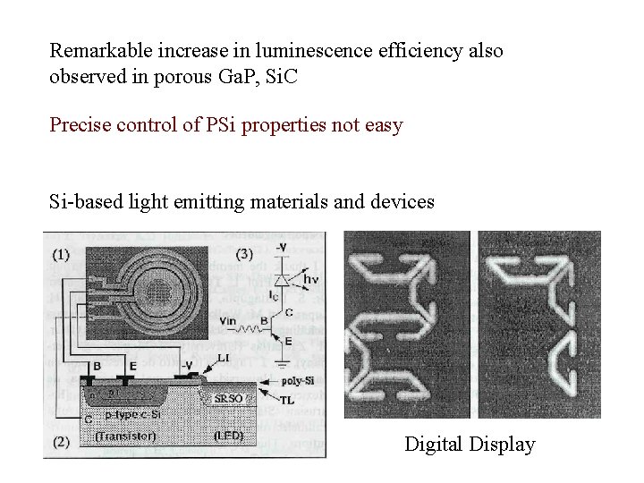
Remarkable increase in luminescence efficiency also observed in porous Ga. P, Si. C Precise control of PSi properties not easy Si-based light emitting materials and devices Digital Display

Atomic structures of carbon nanotubes Stable bulk crystal of carbon Graphite Layer structure: strong intra-layer atomic bonding, weak inter-layer bonding 3. 4 Å 1. 42 Å

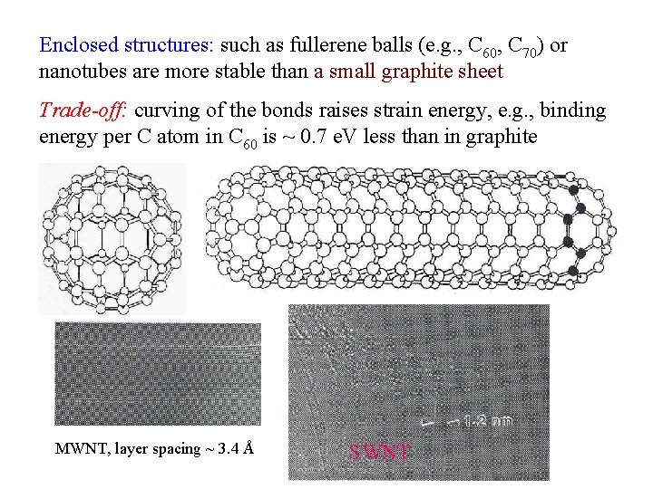
Enclosed structures: such as fullerene balls (e. g. , C 60, C 70) or nanotubes are more stable than a small graphite sheet Trade-off: curving of the bonds raises strain energy, e. g. , binding energy per C atom in C 60 is ~ 0. 7 e. V less than in graphite MWNT, layer spacing ~ 3. 4 Å SWNT

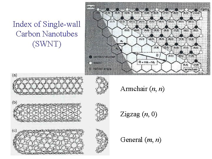
Index of Single-wall Carbon Nanotubes (SWNT) Armchair (n, n) Zigzag (n, 0) General (m, n)

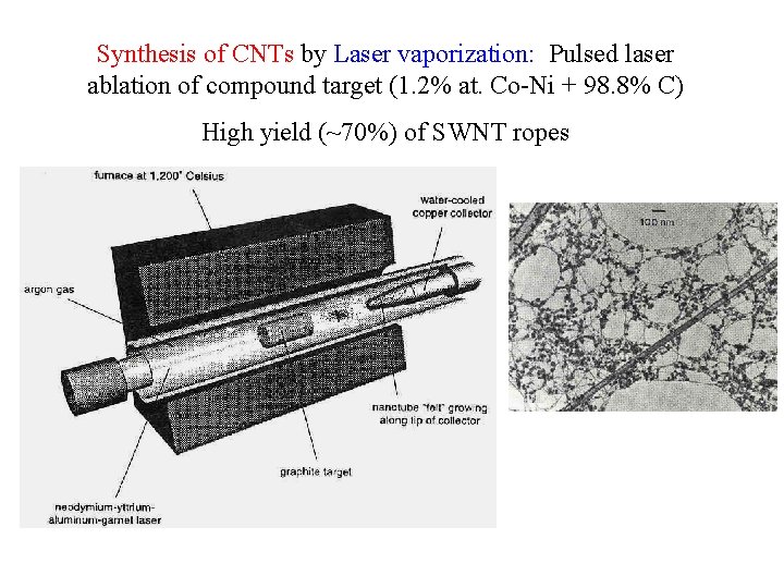
Synthesis of CNTs by Laser vaporization: Pulsed laser ablation of compound target (1. 2% at. Co-Ni + 98. 8% C) High yield (~70%) of SWNT ropes

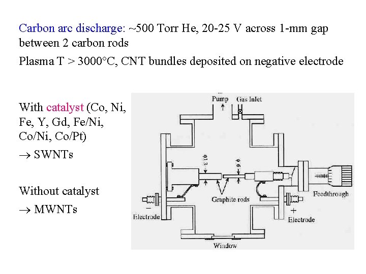
Carbon arc discharge: ~500 Torr He, 20 -25 V across 1 -mm gap between 2 carbon rods Plasma T > 3000 C, CNT bundles deposited on negative electrode With catalyst (Co, Ni, Fe, Y, Gd, Fe/Ni, Co/Ni, Co/Pt) SWNTs Without catalyst MWNTs

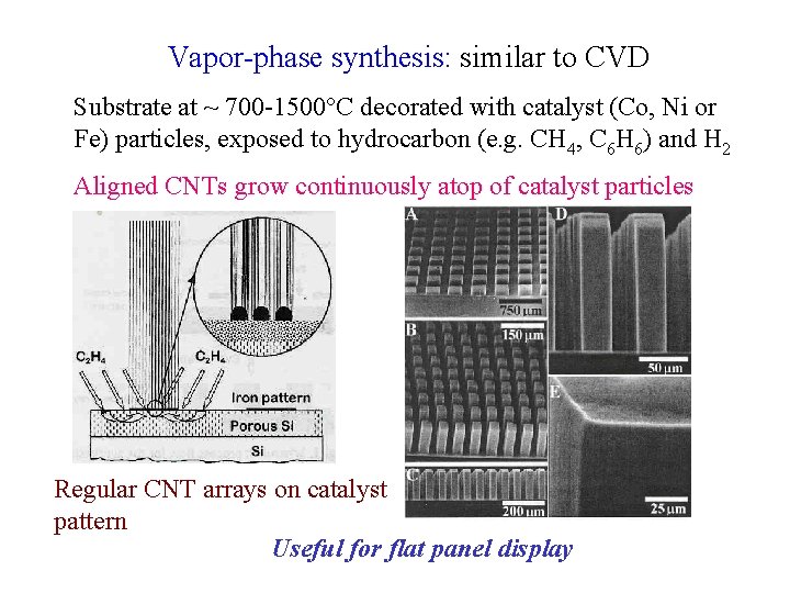
Vapor-phase synthesis: similar to CVD Substrate at ~ 700 -1500 C decorated with catalyst (Co, Ni or Fe) particles, exposed to hydrocarbon (e. g. CH 4, C 6 H 6) and H 2 Aligned CNTs grow continuously atop of catalyst particles Regular CNT arrays on catalyst pattern Useful for flat panel display

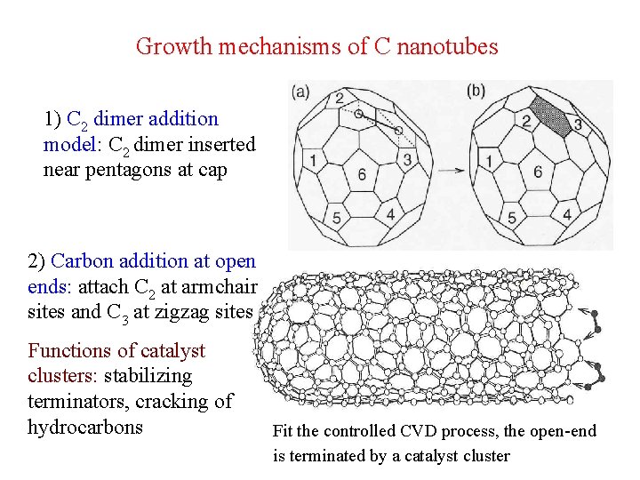
Growth mechanisms of C nanotubes 1) C 2 dimer addition model: C 2 dimer inserted near pentagons at cap 2) Carbon addition at open ends: attach C 2 at armchair sites and C 3 at zigzag sites Functions of catalyst clusters: stabilizing terminators, cracking of hydrocarbons Fit the controlled CVD process, the open-end is terminated by a catalyst cluster

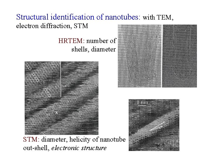
Structural identification of nanotubes: with TEM, electron diffraction, STM HRTEM: number of shells, diameter STM: diameter, helicity of nanotube out-shell, electronic structure

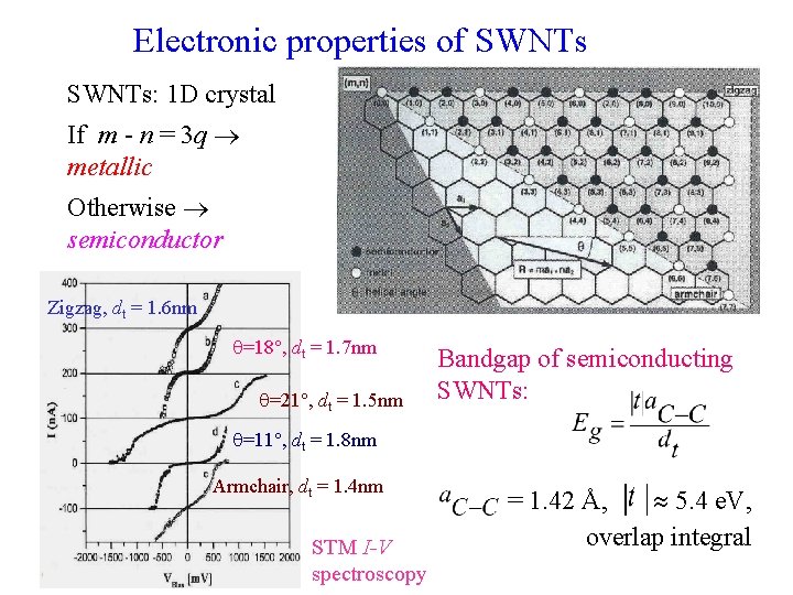
Electronic properties of SWNTs: 1 D crystal If m - n = 3 q metallic Otherwise semiconductor Zigzag, dt = 1. 6 nm =18 , dt = 1. 7 nm =21 , dt = 1. 5 nm Bandgap of semiconducting SWNTs: =11 , dt = 1. 8 nm Armchair, dt = 1. 4 nm STM I-V spectroscopy = 1. 42 Å, 5. 4 e. V, overlap integral

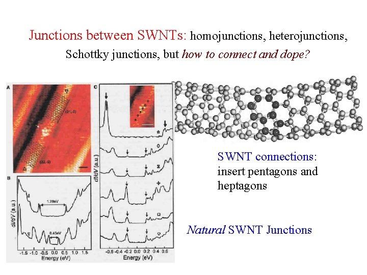
Junctions between SWNTs: homojunctions, heterojunctions, Schottky junctions, but how to connect and dope? SWNT connections: insert pentagons and heptagons Natural SWNT Junctions

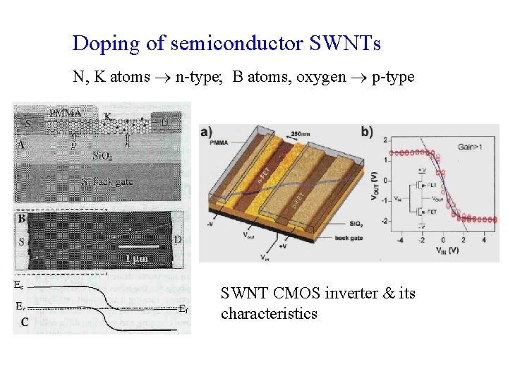
Doping of semiconductor SWNTs N, K atoms n-type; B atoms, oxygen p-type SWNT CMOS inverter & its characteristics

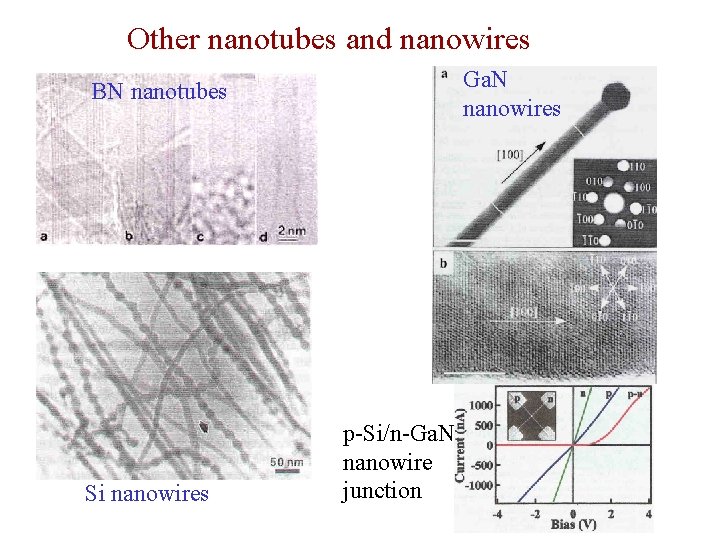
Other nanotubes and nanowires Ga. N nanowires BN nanotubes Si nanowires p-Si/n-Ga. N nanowire junction