Semiconductors and Doping Semiconductors Revisited Properties These are


 are generated. These EHPs are the only")


- Slides: 18
Semiconductors and Doping
Semiconductors Revisited Properties • These are inorganic materials made from elements in the fourth column (Group IV) of the periodic table. Semiconductors in Group IV are called elemental semiconductors. • Compound semiconductors are made up of Group III and Group V elements or Group II and Group VI elements. • The name semiconductors is because at certain temperatures they are good electrical conductors, and they are insulators in other temperature ranges.
The most important semiconductor is Si because of its wide use in IC and MEMS fabrication. - Si crystallizes in diamond lattice. - Each Si atom has four equi-distant nearest neighbors. - The lattice constant for Si is 5. 43 Å.
Crystal Characterization The grown Si wafer differs from an ideal crystal in many ways : • It is finite so surface atoms are not completely bonded. • It has defects such as : (I) point defects, (ii) line defects, (iii) area defects, and (iv) volume defects.
Czochralski Silicon : Electrical Properties
Mechanical Properties of Si
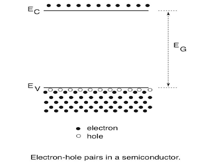
Intrinsic Semiconductors - A perfect semiconductor crystal with no impurities or structural defects is called an intrinsic semiconductor. - In this material there are no charge carriers at 0 K.
- At higher temperatures electron-hole pairs (EHPs) are generated. These EHPs are the only charge carriers in intrinsic material. - Since the electrons and holes are created in pairs ; no = po = ni , ni is the intrinsic carrier concentration
- In equilibrium, at the same rate in which they are generated recombination of EHPs take place at a rate r (EHPs/unit volume/unit time) : r = a no po = a ni 2 - The EHP generation rate at equilibrium g is : r = g = a no po = a ni 2
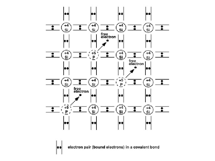
Extrinsic Semiconductors - It is possible to create carriers in semiconductors by purposely introducing impurities into the crystal: this process is called doping. - When a crystal is doped the material is said to be extrinsic. - There are two types of doping; n-type and ptype.
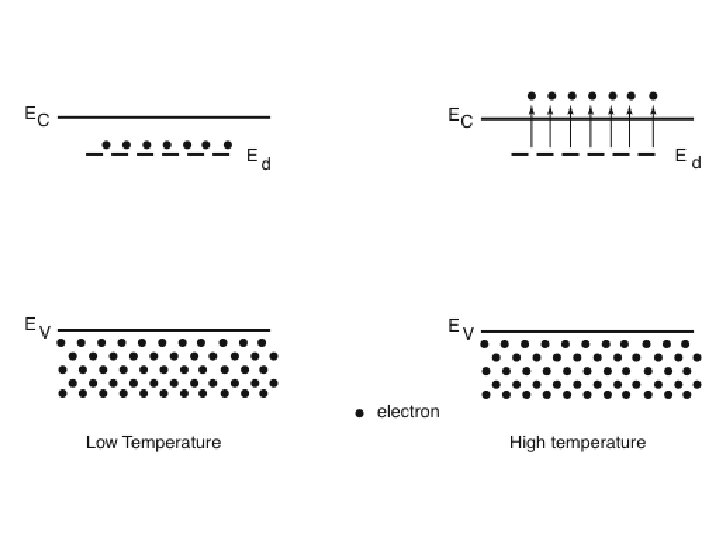
N-Type Semiconductor - Elemental semiconductor, e. g. Si, doped with Group V impurity such as P to a level of Nd per unit volume. - Group V atom is a "donor" and its level in the energy gap, Ed , is called donor level or state. - In n-type no >> po, and if all donors donate electrons then no ~ Nd.
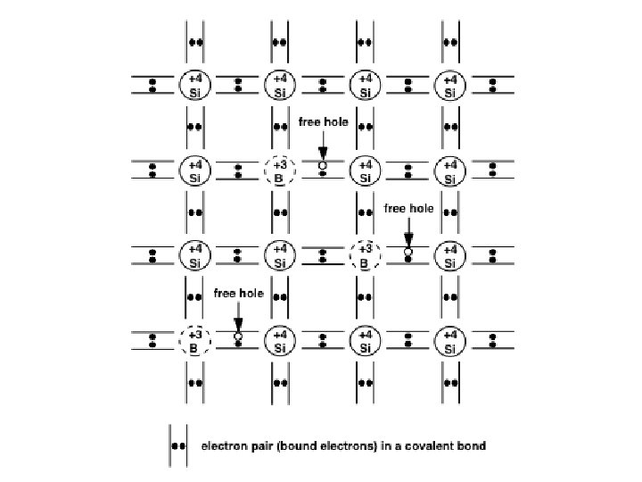
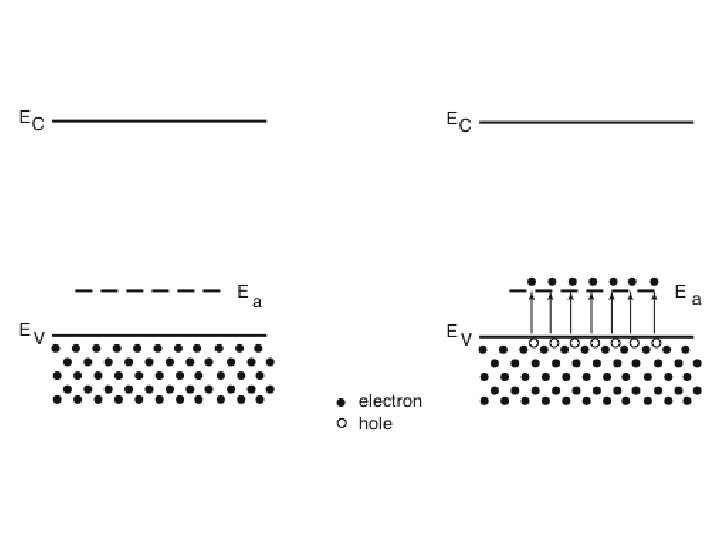
P-Type Semiconductor - Elemental semiconductor, e. g. Si, doped with Group III impurity such as B to a level of Na per unit volume. - Group III atom is ”acceptor" and its level in the energy gap, Ea , is called acceptor level or state. - In p-type po>>no, and if all acceptors accept electrons then po ~ Na.
Counter-Doping/Compensation