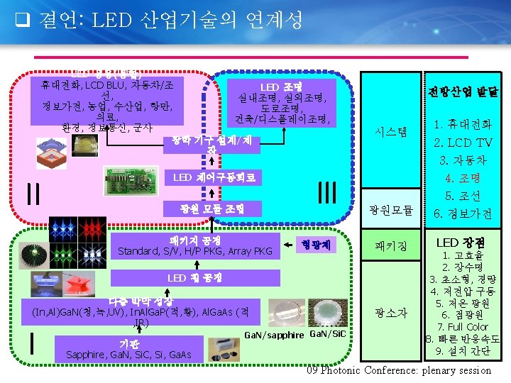
q LED Value Up Point Picture Quality ECO


")

 기술 : LED Chip + 형광체 +")


 Advantages: 1)")
 DX center causes I-V collapse at")
 Pseudomorphic HEMT: Al. Ga. As/In. Ga. As, Al. In. As/In.")
 SL HEMT, proposed by Baba in 1983, using Al. As/Ga.")
 Planar doped HEMT, proposed by Eastman in 1983, a few")

- Slides: 23
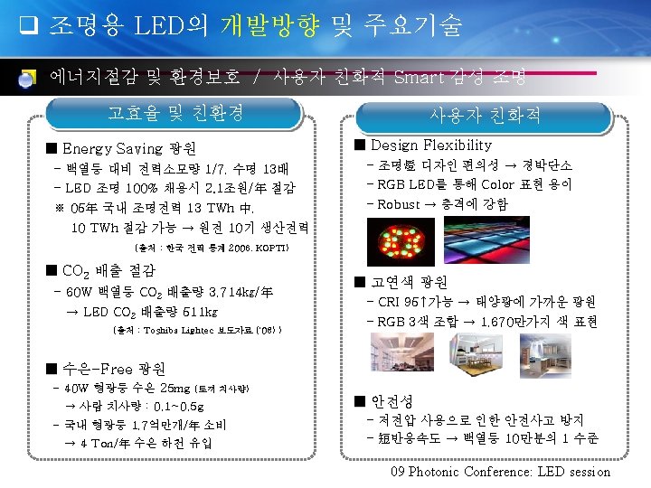
q 디스플레이용 LED 개발방향 및 주요기술 Value Up Point? - Picture Quality, ECO, Slim 2, 000: 1 Color Gamut Contrast § Scanning / Local Dimming § 色 再現性 Contrast 5, 000: 1 (CCFL 72%, LED 78~95%) Slim化 80, 000: 1 ` § CCFL : ~ 105 mm Super Slim LED TV : 20 mm↓ [ '09年 Edge형 LED Model] - CCFL比 消費電力 40% ↓ 實現 Size CO 2 Down 40” 46” ‘ 08 '09 ‘ 10 CCFL Direct LED Edge LED 180 W 120 W 85 W 70 W 215 W 135 W 95 W 77 W * 120 Hz 기준 09 Photonic Conference: LED session
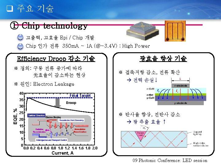
q 주요 기술 ① Chip technology 高휘도, 高출력 LED개발 → 저 소비전력 구현 주로 middle Power 이하 Chip 사용 - Mobile @20 m. A, 대형 display용 @100~300 m. A 구동 2005年 ~ 低출력 백색 LED(@20 m. A) 50 150 lm/W 2010年 ~ 高출력 LED(@100~300 m. A) 150 200 lm/W 以上↑ ※ RG형광체 경우 30% 효율 저하 예상 개발 방향 ◈ 내부양자효율(IQE) 향상 - Epi: 결정성 향상, MQW 구조 최적화 - Chip: 전극구조 최적화 결정성 향상 ◈ 외부 추출효율 향상 Patterned Wafer [EPI up구조] -Surface pattering [Flip, Thin Ga. N 구조] - Chip : P-Ga. N roughening, n-Ga. N &ITO patterning 적용 - 고 방열 수직 구조 기판(Al 2 O 3) 사용 P-Ga. N roughening 09 Photonic Conference: LED session
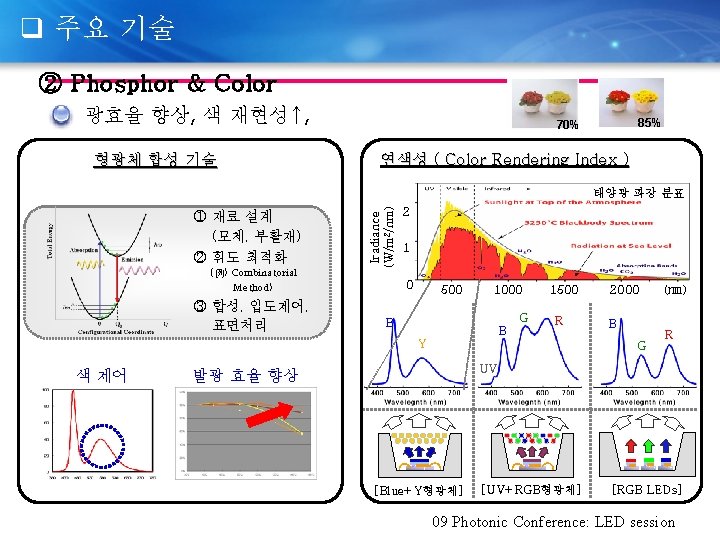
q 주요 기술 ② 형광체 기술 색 재현성↑, 효율 향상 新 형광체 (Red, Green형광체) Red Green Phosphor with Yag, Silicate계열 Quantum Dot 재질 (1 st Gen. ) (2 nd Gen) Blue LED Wide Color Gamut White LED NTSC 比 115% 110 NTSC 比 95% 90 반치폭(nm) 색재현성(%) Deep Green쪽으로 확장 Deep Red 쪽으로 확장 v’ 현재 NTSC 比 78% 60 ’ 09 현재 ‘ 11 20 ‘ 15 년도 u’ 09 Photonic Conference: LED session
q 주요 기술 ③ Package Technology -Life Time Package Design for display 구조 관점 설계 인자 재료 관점 설계 인자 열 전달 구조 단순 Lead frame 구조 Chip Molding compound mold § Durable to high temp. § Highly reflective L/F [변색방지] [열저항 : 30 K/W] 열 전달 구조 복잡 Lead frame 구조 Encapsulation Chip mold § Highly Reliable Silicone Lead Frame § Resistant to UV, high humidity & temp. [변색] [열저항 大 : 80 K/W] Thermal Resistance § Lead frame contacts PCB directly § ~ 40 K/W (@ 60 m. A) 09 Photonic Conference: LED session
q 주요 기술 ③ Package Technology 집적(Integration) 기술 : LED Chip + 형광체 + 봉지재 + 렌즈 + 몰드(컵) Optical, Thermal, Color Design & Process Tech. Optical Lens Adaption : Durable to high temp. : Highly Optical efficiency With Dome Lens Thermal Management Color Distribution : Solution For Bull’s Eye effect. (a) L/F Type (b) Ceramic PKG : Conformal Phosphor Coating : White Chip solution < Bull’s Eye > : Lowering the power consumption !! : Incrase Life Time !!! 09 Photonic Conference: LED session
History of HEMT - An idea of using heterostructure, proposed by W. Shockley - High mobility of 2 D gas, predicted by Esaki & Tsu, 1969 Advancement of Epitaxial Growth Techniques, MBE (atomically flat interface, abrupt doping profile, high crystal quality) - 2 D gas, experimentally proven by Dingle et al. , 1978 - Al. Ga. As/Ga. As HEMT, fabricated by Mimura et al. , 1980 - HET (Hot Electron Transistor), Heiblum et al. , 1981 - RHET (Resonant Tunneling HET), Yokoyama et al. , 1985 HEMT 관련: Semiconductor & semimetals, Vol. 30 12
Temperature dependence of ‘e’ mobility for high purity Ga. As with n = 2. 7 x 1013 cm-3 ‘e’ mobility of Ga. As=4800 cm 2/Vsec @RT It becomes as great as 300, 000 @40 K due to the decrease of polar-optical and iezoelectric-acoustic phonon scattering. Below 40 K, it decreases steeply to ~ 9000 But, the problem is low conductivity of u-Ga. As. If increasing doping, mobility @40 K ~@RT due to impurity scattering. Need for semiconductor materials with both high mobility and high carrier concentration modulation-doped superlattice, proposed by Esaki and Tsu A key technology for the success of HEMT is (Si dopint is abrupt doping profile, low diffusion) HEMT 관련: Semiconductor & semimetals, Vol. 30 13
Modulation Doping spacer HEMT 관련: Semiconductor & semimetals, Vol. 30 14
Al. Ga. As/Ga. As HEMT Surface depletion Interface depletion HEMT 관련: Semiconductor & semimetals, Vol. 30 15
2 DEG properties are determined by -Spacer layer thickness -Background impurity concentration in the Ga. As region -Si doping concetration in n-Al. Ga. As -Al mole fraction in Alx. Ga 1 -x. As (x) Temperature dependence of ‘e’ mobility 16 30 and sheet concentration HEMT 관련: Semiconductor & semimetals, Vol.
2 DEG vs. spacer layer thickness -The most effective parameter for increasing 2 DEG mobility at low temperature -Under illumination, 2 DEG concentration increases to ~ twice the original due to the PPC effect Two limiting factors of 2 DEG mobility Under illumination In the dark (1) Remote impurity scattering of 2 DEG by Si impurities in n-Al. Ga. As is reduced with increasing the thickness, increased ‘e’ mobility (2) 2 DEG concentration decreases with increasing the thickness, resulting in enhanced ionized-impurity scattering and reduced ‘e’ mobility At the early stage, spacer thickness < 10 nm due to the scattering center in Al. Ga. As All the Si impurities and not electrically active in Al. Ga. As for Nsi > 4 x 1018 cm-3 due to PPC HEMT 관련: Semiconductor & semimetals, Vol. 30 17
Ga. As/n-Al. Ga. As HEMT (by Mimura et al. , 1980 ) Advantages: 1) High mobility – due to spatial separation between mobile carriers in channel and parent ionized donor impurities. 2) High transconductance – due to high sheet concentration (2 D gas in HEMT ~ inversion layer in MOSFET, but effective mass of Ga. As is very small (0. 06 m e), leading to significant quantum effect Ef moves up to CB edge high sheet concentration. - due to small separation between gate and channel (Cg increase fm, f. T increase) 3) Higher turn-on voltage for the gate current, reducing the gate leakage Disadvantages: due to the DX center (or dopant induced traps) - Small voltage swing (Vg-Vt) - Large Vt shift with temperature - PPC, etc. HEMT 관련: Semiconductor & semimetals, Vol. 30 18
Limitations of Ga. As/n-Al. Ga. As HEMT (1) DX center causes I-V collapse at low temperature and thermal instability of the Vth of a HEMT (2) Small conduction-band edge discontinuity, leading to insufficient, low 2 DEG concentration (3) Thermally unstable layer structures with respect to diffusion of Si from the n-Al. Ga. As layer into the Ga. As channel region difficult to anneal these materials. flash-lamp annealing using Ga. As stopper layer (to prevent the penetration of 2 DEG wavefunction into the Ga. As (with a small diffusivity) stopper layer HEMT 관련: Semiconductor & semimetals, Vol. 30 19
Progress in HEMT (1) Pseudomorphic HEMT: Al. Ga. As/In. Ga. As, Al. In. As/In. Ga. As structures: Advantages: by making a junction between two materials with a large discontinuity, - produced a large QW increasing the electron density - Free of DX center high doping becomes possible high gm - High mobility of In. Ga. As. Disadvantages: high gate leakage current Low VBD HEMT 관련: Semiconductor & semimetals, Vol. 30 20
Progress in HEMT (2) SL HEMT, proposed by Baba in 1983, using Al. As/Ga. As SL instead of Al. Ga. As layer - dopants are incorporated in the Ga. As QW. - DX center is eliminated HEMT 관련: Semiconductor & semimetals, Vol. 30 21
Progress in HEMT (3) Planar doped HEMT, proposed by Eastman in 1983, a few tens of A Si doping is made in a Ga. As layer symmetric and asymmetric type 22 HEMT 관련: Semiconductor & semimetals, Vol. 30
Enhancement/Depletion-Mode n-HEMTs E-mode D-mode HEMT 관련: Semiconductor & semimetals, Vol. 30 23