CHM 585490 Chapter 19 Semiconductors 1 Semiconductors The


- Slides: 31

CHM 585/490 Chapter 19 Semiconductors 1

Semiconductors • The market for imaging chemicals – photoresists, developers, strippers, and etchants – for the combined semiconductor and printed wiring board applications is in excess of $3 billion 2

Moore’s Law 3

Moore’s Law • It’s not a Law of Nature, but it comes close. In 1965, Intel co-founder Gordon Moore made the observation that has become known as Moore’s Law: the number of devices on a single chip (and the chip’s potential performance) doubles every year or so. 4

• Integrated circuits – millions of transistors layered on fingernail-sized chips of silicon. • After 30 years of operation under Moore’s Law, manufacturers have reduced circuit patterns to incredibly thin line widths – pushing 0. 18 microns, less than 1/160 the width of a human hair. 5

6

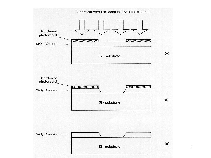
7

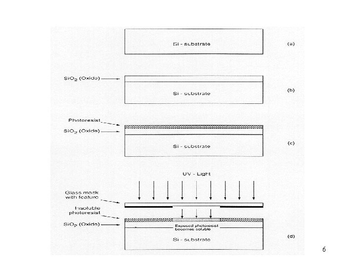
Lithography • Photosensitive polymer film is exposed to light to alter the solubility. • If the exposed area of the resist film becomes insoluble after light exposure, then the resist is termed “negative” • If the exposed area becomes more soluble – ‘positive” photoresist 8

Photoresists • In certain applications, the film becomes a permanent, functional component of the device being constructed, typically serving as an electrical insulator or protective encapsulant • Most commonly, the resist is removed or “stripped” after the image has been transferred to the substrate. 9

Essential Attributes of Lithographic Resists • Must form uniform defect-free films on the substrate • Coated film must display adequate adhesion to the substrate • Must have suitable radiation sensitivity. Exposure tools are so costly that throughput is a key measure of performance. 10

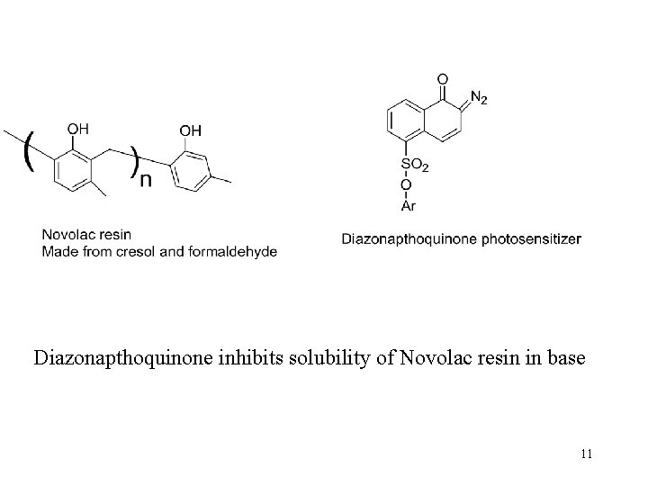
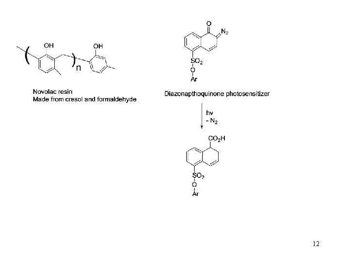
Diazonapthoquinone inhibits solubility of Novolac resin in base 11

12

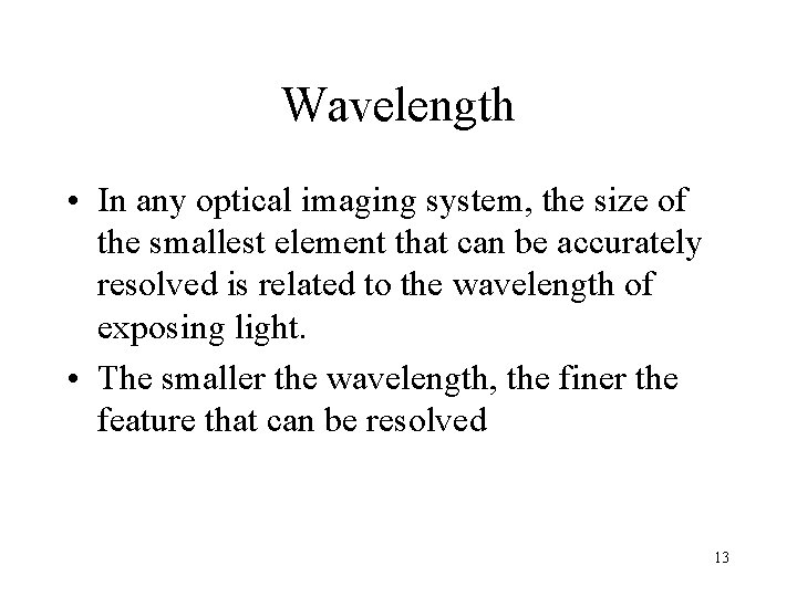
Wavelength • In any optical imaging system, the size of the smallest element that can be accurately resolved is related to the wavelength of exposing light. • The smaller the wavelength, the finer the feature that can be resolved 13

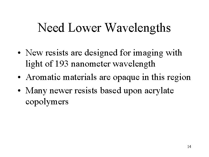
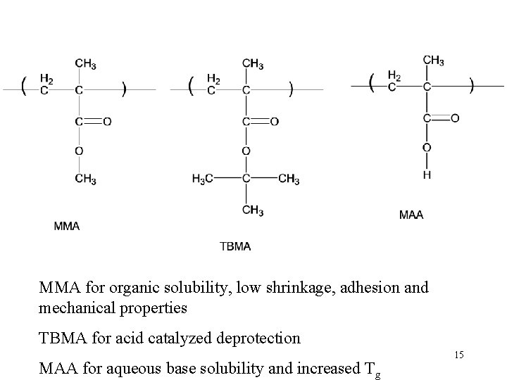
Need Lower Wavelengths • New resists are designed for imaging with light of 193 nanometer wavelength • Aromatic materials are opaque in this region • Many newer resists based upon acrylate copolymers 14

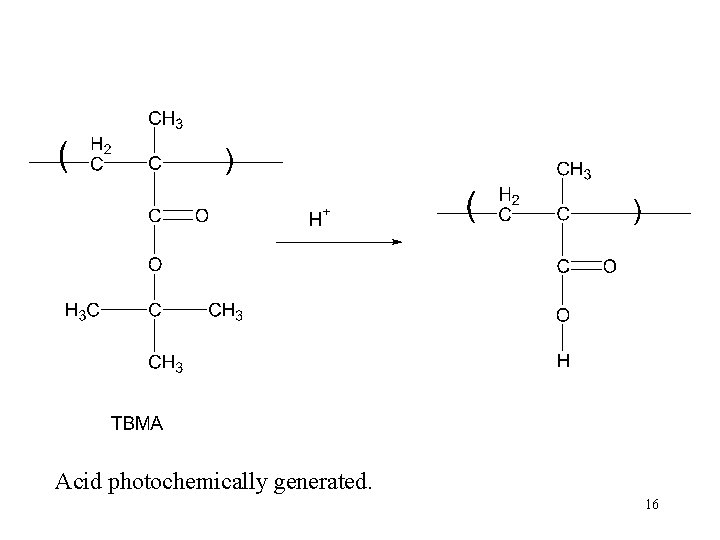
MMA for organic solubility, low shrinkage, adhesion and mechanical properties TBMA for acid catalyzed deprotection MAA for aqueous base solubility and increased Tg 15

Acid photochemically generated. 16

Many other uses for polymers in microelectronic applications • • Adhesives Conductive adhesives Interlayer dielectrics Glob Top 17

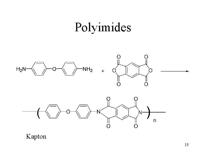
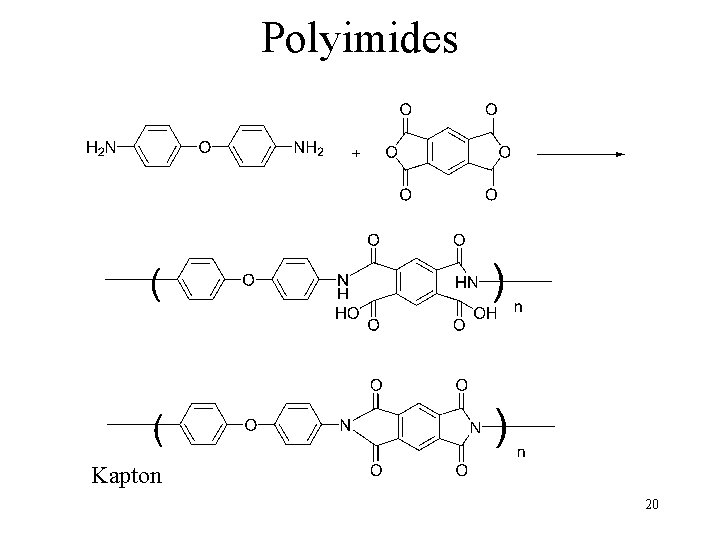
Some microelectronic polymers • • Polyimides Epoxies BCBs Parylenes 18

Polyimides Kapton 19

Polyimides Kapton 20

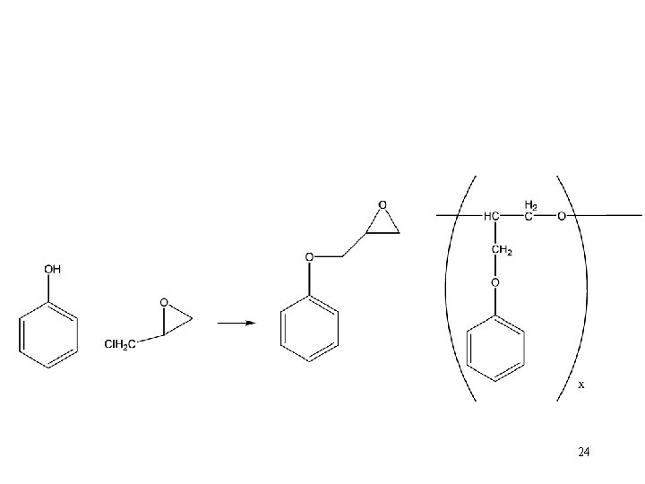
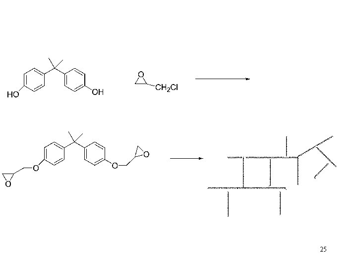
Epoxies • Epoxy resins are high-performance thermosetting resins. High performance coatings continue to be the primary application worldwide; electrical-electronic laminates, adhesives, flooring and paving applications, composites, and tooling and molding products are the other major end uses. Industrialized nations are by far the largest producers and consumers of epoxy resins 21

• In 1999, the estimated epoxy resin production value for the United States, Western Europe and Japan was over $2 billion. • In 1999, almost 650 thousand metric tons of epoxy resins were consumed in the United States, Western Europe and Japan combined. Between 1999 and 2004, overall growth in epoxy resin demand is expected to average about 3. 2% per year in the United States 22

• The three leading producers of epoxy resins are Resolution (formerly Shell's Epoxy Resins and Versatics business), Dow and Vantico. Together they account for approximately 75% of the world's capacity. 23

24

25

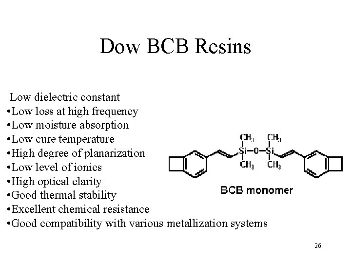
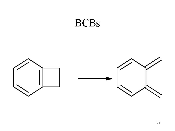
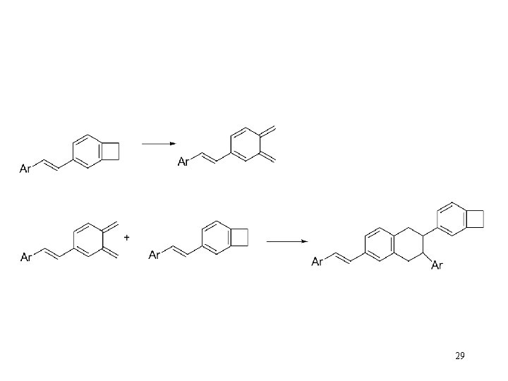
Dow BCB Resins Low dielectric constant • Low loss at high frequency • Low moisture absorption • Low cure temperature • High degree of planarization • Low level of ionics • High optical clarity • Good thermal stability • Excellent chemical resistance • Good compatibility with various metallization systems 26

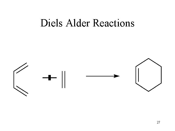
Diels Alder Reactions 27

BCBs 28

29

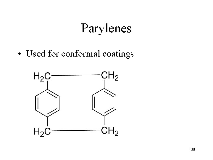
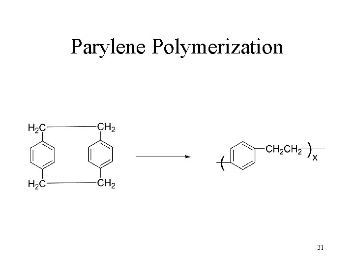
Parylenes • Used for conformal coatings 30

Parylene Polymerization 31