Semiconductor Physics Behind Detectors Saif Ullah Awan Ph

Semiconductor Physics Behind Detectors Saif Ullah Awan, Ph. D Assistant Professor Department of Electrical Engineering National University of Sciences and Technology (NUST) Islamabad

Out Line • • • Types of semiconductors Bond model and band model approach Drift velocity, mobility and resistivity Comparison of different semiconductors PN Junction

Advantages / Disadvantages of semiconductor detectors

Constructing a detector

Constructing a detector

Elemental Semiconductor

Elemental Semiconductor

Why Silicon is more common semiconductor

Bond model of semiconductors

Band structure of electron levels Solid → crystalline structure of atoms in a lattice, with covalent bonds. The periodic arrangement of atoms in the crystal causes an overlap of electron wave-functions, which creates a “band” of energy states allowed for the outermost shell energy levels. Electrons are fermions: the Pauli principle forbids to have more than one electron in the same identical state and this produces a degeneracy in the outer atomic shell energy levels. This produces many discrete levels which are very close to each other, which appear as “bands” The innermost energy levels are not modified, and the electrons remain associated to the respective lattice atoms. CONDUCTION BAND: electrons are detached from parent atoms and are free to move about the whole crystal VALENCE BAND: electrons are more tightly bound and remain associated to the respective lattice atom

Energy bands: isolator – semiconductor - metal 1. In an isolated atom the electrons have only discrete energy levels. 2. In solid state material the atomic levels merge to energy bands. 3. In metals the conduction and the valence band overlap, whereas in isolators and semiconductors these levels are separated by an energy gap (band gap). 4. In isolators this gap is large.
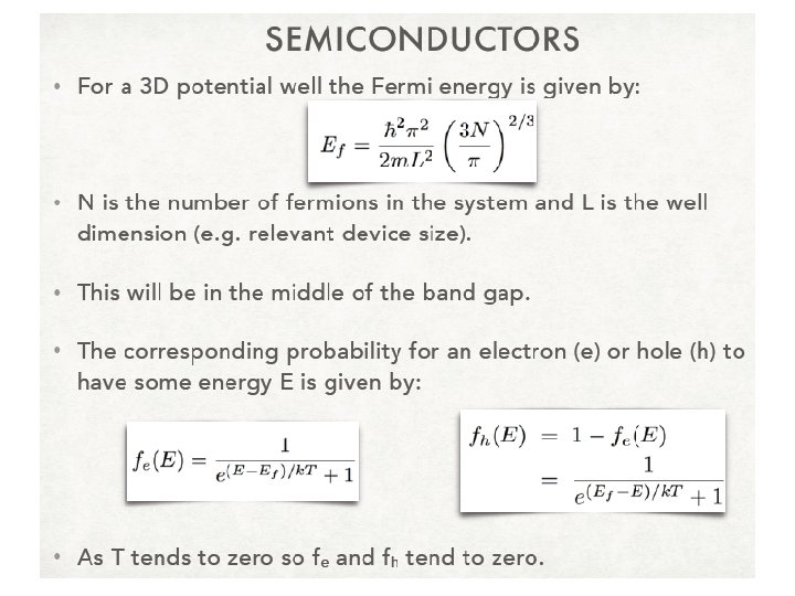

Fermi distribution, Fermi levels

Band theory of solids • The width of the energy bands and the energy gap is determined by the inter-atomic spacing. This depends on temperature and pressure. • Bands determine the density of available energy states

Band theory of solids

Semiconductors: temperature dependence

Charge carriers in semiconductors

Intrinsic semiconductors • An undoped semiconductor is called an intrinsic semiconductor • Crystalline lattice, of tetravalent elements (Si, Ge) • 4 valence electrons → covalent bonds

Intrinsic semiconductors

Drift velocity and mobility

Resistivity

Intrinsic semi-conductor properties

Properties of intrinsic Si and Ge

Comparison of different semiconductors

Comparison of different semiconductors

Recombination and trapping Process Effects of Defects EC EV e e h Generation h Recombination Leakage Current e e h Trapping Charge Collection Compensation Effective Doping Density

Recombination and trapping Process

Doping

Elemental Doping of semiconductors
Energy band structure, (b)carrier concentration (c)occupation probability for intrinsic")
Doping: n- and p-type silicon (a)Energy band structure, (b)carrier concentration (c)occupation probability for intrinsic semiconductors.

Bond model: n-doping in silicon

Band model: n-doping in silicon

Example: n-type doped semiconductors

Bond model: p-doping in silicon

Band model: p-doping in silicon

p-type doped semiconductors

Donor and acceptor levels in Si and Ga. As

p-n junction

p-n junction

p-n junction 1. 2. 3. 4. At the interface of an n-type and p-type semiconductor the difference in the fermi levels cause diffusion of surplus carries to the other material until thermal equilibrium is reached. At this point the fermi level is equal. The remaining ions create a space charge and an electric field stopping further diffusion (contact potential). The stable space charge region is free of charge carries and is called the depletion zone.

p-n junction

p-n junction • Near intrinsic bulk • Highly doped contacts • Apply bias (-ve on p+ contact) – Deplete bulk – High electric field • Radiation creates carriers n+ contact ND=1018 cm-3 ND~1012 cm-3 – signal quanta • Carriers swept out by field – Induce current in external circuit signal p+ contact NA=1018 cm-3
 = 23 k")
Why a diode? • Signal from MIP (Minimum ionizing particles ) = 23 k e/h pairs for 300 mm device • Intrinsic carrier concentration – ni = 1. 5 x 1010 cm-3 – Si area = 1 cm 2, thickness=300 mm 4. 5 x 10⁸ electrons – 4 orders > signal • Need to deplete device of free carriers • Want large thickness (300 mm) and low bias But no current! – Use v. v. low doped material – p+ rectifying (blocking) contact
 p+ n (5) (2) Carrier density Electric field (6) (3) Dopant")
p-n junction (1) p+ n (5) (2) Carrier density Electric field (6) (3) Dopant concentration (4) Space charge density PPE S/C detector lectures (7) Dr R. Bates Electric potential 44
 take your samples – these are neutral but doped samples: p+")
p-n junction 1) take your samples – these are neutral but doped samples: p+ and n 2) bring together – free carriers move o two forces drift and diffusion o In stable state Jdiffusion (concentration density) = Jdrift (e-field) 3) p+ area has higher doping concentration (in this case) than the n region
 5) Fixed charge region Depleted of free carriers o o Called")
p-n junction 4) 5) Fixed charge region Depleted of free carriers o o Called space charge region or depletion region Total charge in p side = charge in n side Due to different doping levels physical depth of space charge region larger in n side than p side Use n- (near intrinsic) very asymmetric junction 6) Electric field due to fixed charge 7) Potential difference across device o Constant in neutral regions.

p-n junction: forward bias Applying an external voltage V with the anode to p and the cathode to n e- and holes are refilled to the depletion zone. The depletion zone becomes narrower. The potential barrier becomes smaller by e. V and diffusion across the junction becomes easier. The current across the junction increases significantly.

p-n junction: reverse bias Applying an external voltage V with the cathode to p and the anode to n e- and holes are pulled out of the Depletion zone. The depletion zone becomes larger. The potential barrier becomes higher by e. V and diffusion across the junction is suppressed. The current across the junction is very small “leakage current”.

Width of depletion zone

p-n junction: leakage current

Acknowledge 1. Semiconductor detectors by Silvia Masciocchi, GSI Darmstadt and University of Heidelberg 39 th Heidelberg Physics Graduate Days, HGSFP Heidelberg 2. Indian Institute of Technology Hans-Jürgen Wollersheim 3. Gerhard Lutz, Semiconductor, Radiation Detectors Device Physics

THANK YOU FOR ATTENTION
- Slides: 52