Flash memory Flash memory is a nonvolatile storage

 device. Ø Electrons")
 transistors 1.")


 here 21")


 37")


- Slides: 43
Flash memory Ø Flash memory is a non-volatile storage device that can be electrically erased and reprogrammed. 圖片摘自https: //www. shutterbug. com/content/digital-media-guide-portable-digital-media-computers-digital-camerasand-other-devices 1
Neo Flash Ø Neo Flash is a type of Silicon-Oxide-Nitride. Oxide-Silicon(SONOS) device. Ø Electrons are stored in the Oxide-Nitride. Oxide(ONO) film. Ø Advantages (優點) 1. Simple cell structure 2. lower process integration complexity 3. low operating voltage 4. low cost 2
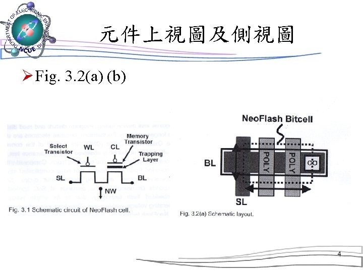
Basic cell structure Ø Fig. 3. 1 Ø Two p-channel MIS (metal/insulator/silicon) transistors 1. p MOST : select transistor 2. SONOS-gate p-channel FET : memory transistor 3
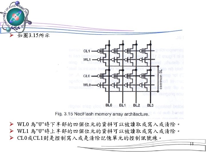
Neo. Flash memory array architecture Ø Fig. 3. 15 Ø SL : sourceline Ø BL : bitline 5
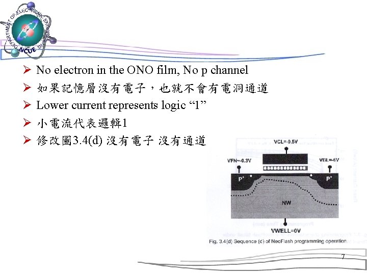
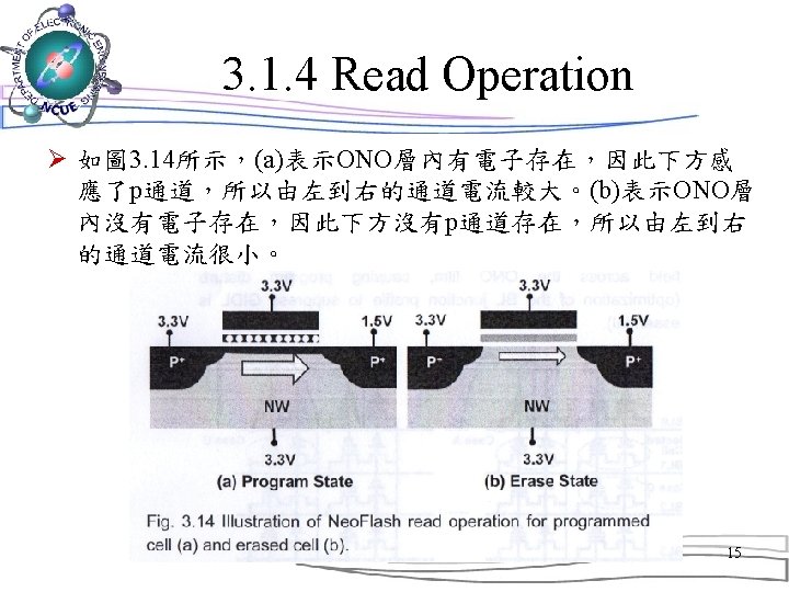
Ø p-channel uses holes to conduct currents Ø P通道以電洞來傳導電流 Ø Ø Ø Electrons stored in the ONO film and induced a p channel 如果記憶層存有電子將會在其下方感應出電洞通道 Higher current represents logic “ 0” 大電流代表邏輯 0 如圖 3. 4(d) Ø Ø No electron in the ONO film, No p channel 如果記憶層沒有電子,也就不會有電洞通道 Lower current represents logic “ 1” 小電流代表邏輯 1 6
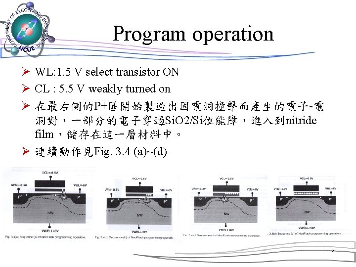
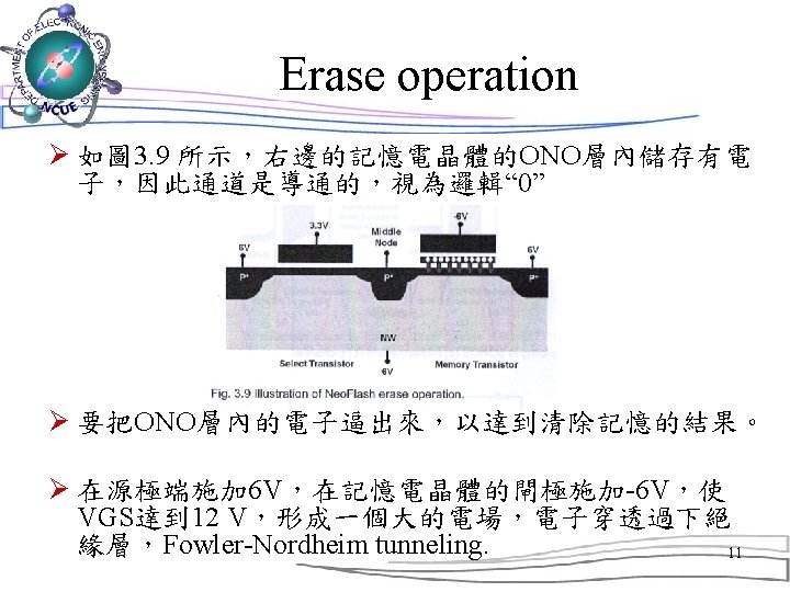
Program operation Ø Fig. 3. 3 Ø WL : word line Ø CL : cell control line Ø BL : bit line Ø CSL : common source line Ø NW : n-well 8
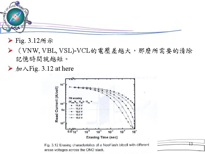
Ø P-channel SONOS結構能比較有效地防止p+ poly的電子穿隧 進入到nitride層,因此P-channel SONOS結構比n-channel SONOS結構更適合用來做為Flash Memory Ø Fig. 3. 11 12
3. 1. 5 Array Architecture Ø 如圖 3. 15所示 16
Ø 一個記憶體由兩個電晶體組成,一個是p-channel select transistor,另一個是p-channel memory transistor, 兩者 都是置於n-well Ø 每個記憶單元有四條線 Ø WL: word line Ø CL: cell control line Ø BL: bit line Ø CSL: common source line 17
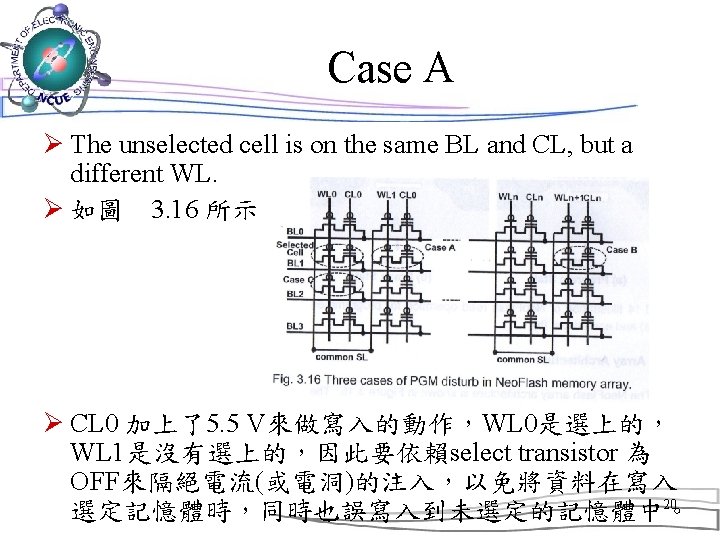
3. 1. 6 Array Disturb ØDisturb is defined as the influence of the operation of selected memory transistors on unselected memory transistors in the same array. Ø主要發生在資料寫入一個電晶體時對其 他記憶電晶體所造成的影響。 ØCase A: 19
Case A Ø Put the Fig. 3. 17(a) here 21
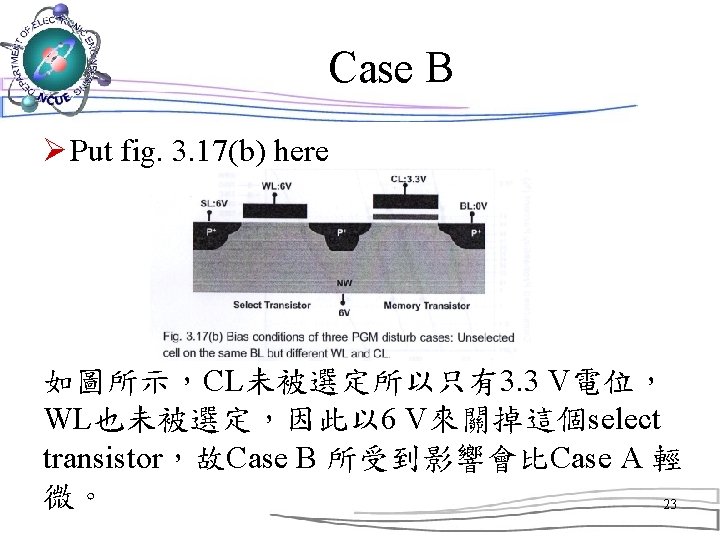
Case B Ø Put Fig. 3. 16 here Ø 如fig 3. 16 右圖所示 Ø The unselected cell is on the same BL, but a different WL and CL Ø 被選定的是WL 0, CL 0,受影響的是WLn+1, CLn 22
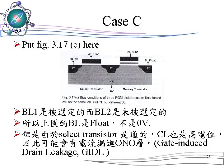
Case C Ø Put the fig. 3. 16 here Ø The unselected cell is on the same WL and CL, but a different BL. Ø WL 0, CL 0是被選定的所以其相對應的WL為 1. 5 V(不是 6 V), CL為 5. 5 V. Ø BL 1是被選定的而BL 2是未被選定的 24
3. 1. 7 Endurance Ø The program and erase operations will introduce electron trapping or oxide damage, which degrade the memory transistor performance. Ø 如Fig. 3. 18 所示 Ø 經過多次的資料寫入與清除後,寫入電流漸漸變小,有如充電 能力減弱了。而清除資料所需要的電流則漸漸變大了。 26
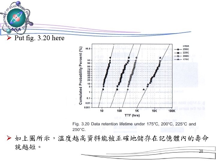
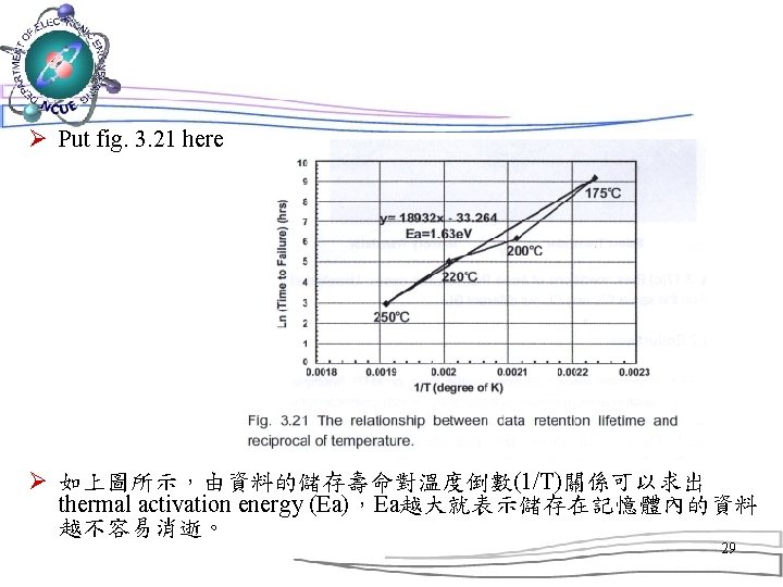
3. 1. 8 Data Retention Ø Data retention is the ability of a memory transistor to keep the stored charges. Ø 如Fig. 3. 19所示: Ø 儲存在Nitride內的電荷可能因為thermionic emission 而穿隧過或越過Oxide的位能障而消逝。 27
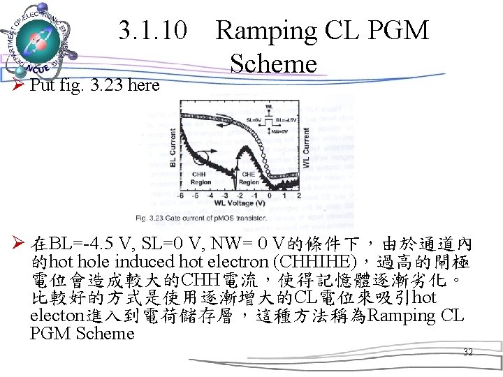
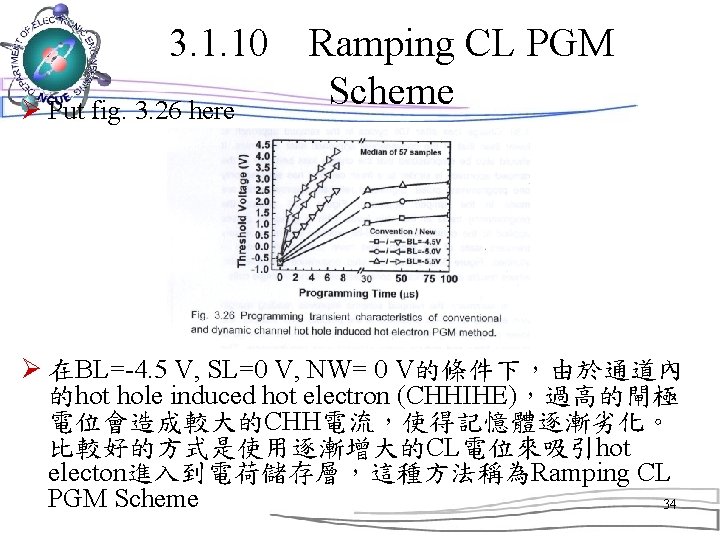
3. 1. 10 Ramping CL PGM Scheme Ø Put fig. 3. 25 here 在WL, BL為負電位,SL及NW為 0電位的偏壓 情況下, 以Ramping CL PGM Scheme方式來寫 33 入資料。
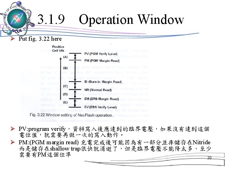
3. 2 Process Integration Ø Put fig. 3. 33 here Ø Neo. Flash is fully compatible with standard logic circuit manufacturing processes. 35
3. 2 Process Integration ØOnly using three additional masks Ø 1. Deep n-well Ø 2. ONO Etch Ø 3. R-ONO Etch 36
3. 2. 1 Isolation Ø Put fig. 3. 35 here Ø 為了減少寄生的漏電流,在基板上做出STI(shallow trench isolation) 37
3. 2. 2 Deep n-Well process Ø Put fig. 3. 36 here Ø 為了製作出programming and erasing high voltages,需要製作Deep n-Well來隔離每一個 p-well, 這些p-Well 內會製作正負電位的 charge pumping circuit 38
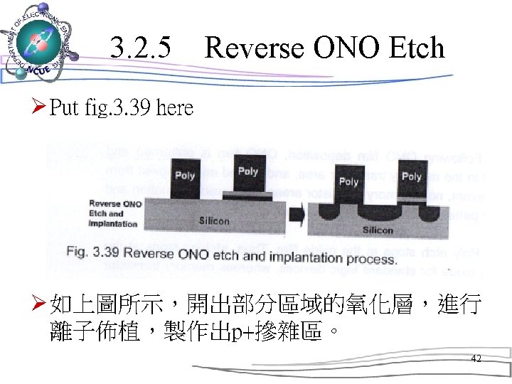
3. 2. 3 ONO Film Formation Ø Put fig. 3. 37 here Ø ONO是三層的材料堆疊而成 Ø Bottom Oxide: 35~40 Å gate oxide 39
3. 2. 3 ONO Film Formation Ø Silicon Nitride: Si 3 N 4 is commonly used as storage layer, which was grown by CVD Ø Top Oxide: Furance oxide or in-situ steam generation (ISSG) oxide Ø Accurate thickness control of the individual ONO layers is the most important consideration. 40
3. 2. 4 Poly Gate Formation Ø Put fig. 3. 38 here Ø 長完ONO層之後要對ONO層做patterning,只在記憶體 電晶體處留下ONO層。 Ø 長上poly層,然後蝕刻成fig. 3. 38右邊的圖案。 Ø Poly etch stops at the oxide film, whereas memory transistor etching stops at the top oxide of the ONO film. 41
論文研讀 Ø Nonvolatile Memory Cells Based on Mo. S 2/Graphene Heterostructures Ø Two-terminal floating-gate memory with van der Waals heterostructures for ultrhigh on/off ratio 43