Introduction to Semiconductor Manufacturing Technology Chapter 1 Introduction
- Slides: 22

Introduction to Semiconductor Manufacturing Technology Chapter 1, Introduction Hong Xiao, Ph. D. hxiao 89@hotmail. com Hong Xiao, Ph. D. www 2. austin. cc. tx. us/Hong. Xiao/Boo k. htm 1

Objective After taking this course, you will able to • • Use common semiconductor terminology Describe a basic IC fabrication sequence Briefly explain each process step Relate your job or products to semiconductor manufacturing process Hong Xiao, Ph. D. www 2. austin. cc. tx. us/Hong. Xiao/Boo k. htm 2

Topics • • Introduction IC Device and Design Semiconductor Manufacturing Processes Future Trends Hong Xiao, Ph. D. www 2. austin. cc. tx. us/Hong. Xiao/Boo k. htm 3

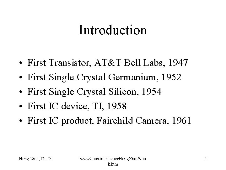
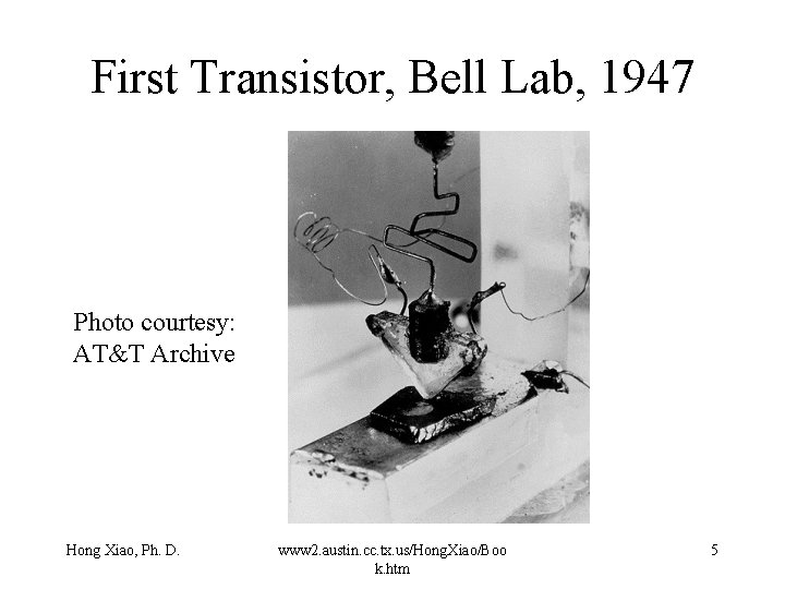
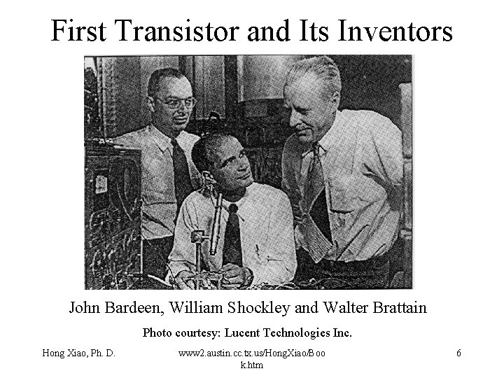
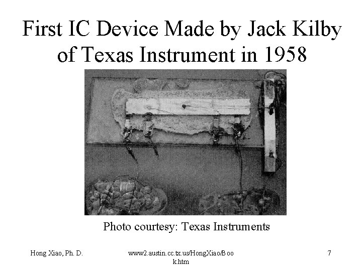
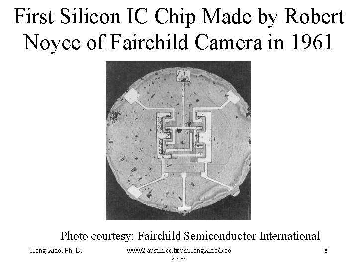
Introduction • • • First Transistor, AT&T Bell Labs, 1947 First Single Crystal Germanium, 1952 First Single Crystal Silicon, 1954 First IC device, TI, 1958 First IC product, Fairchild Camera, 1961 Hong Xiao, Ph. D. www 2. austin. cc. tx. us/Hong. Xiao/Boo k. htm 4

First Transistor, Bell Lab, 1947 Photo courtesy: AT&T Archive Hong Xiao, Ph. D. www 2. austin. cc. tx. us/Hong. Xiao/Boo k. htm 5

First Transistor and Its Inventors John Bardeen, William Shockley and Walter Brattain Photo courtesy: Lucent Technologies Inc. Hong Xiao, Ph. D. www 2. austin. cc. tx. us/Hong. Xiao/Boo k. htm 6

First IC Device Made by Jack Kilby of Texas Instrument in 1958 Photo courtesy: Texas Instruments Hong Xiao, Ph. D. www 2. austin. cc. tx. us/Hong. Xiao/Boo k. htm 7

First Silicon IC Chip Made by Robert Noyce of Fairchild Camera in 1961 Photo courtesy: Fairchild Semiconductor International Hong Xiao, Ph. D. www 2. austin. cc. tx. us/Hong. Xiao/Boo k. htm 8

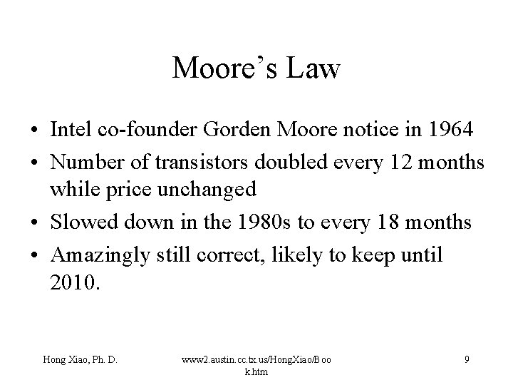
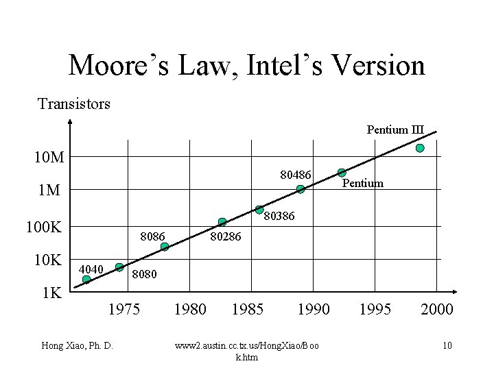
Moore’s Law • Intel co-founder Gorden Moore notice in 1964 • Number of transistors doubled every 12 months while price unchanged • Slowed down in the 1980 s to every 18 months • Amazingly still correct, likely to keep until 2010. Hong Xiao, Ph. D. www 2. austin. cc. tx. us/Hong. Xiao/Boo k. htm 9

Moore’s Law, Intel’s Version Transistors Pentium III 10 M 80486 1 M 80386 100 K 1 K Pentium 8086 4040 80286 8080 1975 Hong Xiao, Ph. D. 1980 1985 1990 www 2. austin. cc. tx. us/Hong. Xiao/Boo k. htm 1995 2000 10

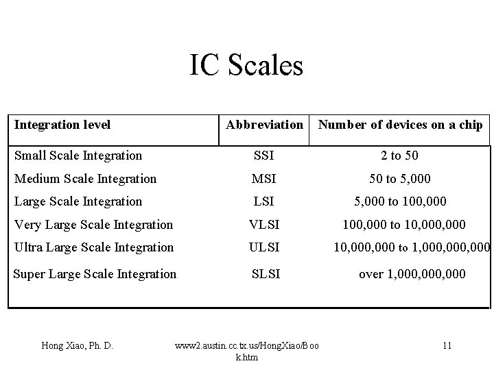
IC Scales Integration level Abbreviation Number of devices on a chip Small Scale Integration SSI 2 to 50 Medium Scale Integration MSI 50 to 5, 000 Large Scale Integration LSI 5, 000 to 100, 000 Very Large Scale Integration VLSI 100, 000 to 10, 000 Ultra Large Scale Integration ULSI 10, 000 to 1, 000, 000 Super Large Scale Integration SLSI over 1, 000, 000 Hong Xiao, Ph. D. www 2. austin. cc. tx. us/Hong. Xiao/Boo k. htm 11

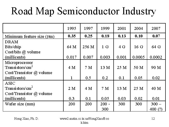
Road Map Semiconductor Industry Minimum feature size (mm) DRAM Bits/chip Cost/bits @ volume (millicents) Microprocessor Transistors/cm 2 Cost/Transistor @ volume (millicents) ASIC Transistors/cm 2 Cost/Transistor @ volume (millicents) Wafer size (mm) Hong Xiao, Ph. D. 1995 1997 1999 2001 2004 2007 0. 35 0. 25 0. 18 0. 13 0. 10 0. 07 64 M 256 M 1 G 4 G 16 G 64 G 0. 017 0. 003 0. 001 0. 0005 0. 0002 4 M 7 M 13 M 25 M 50 M 90 M 1 0. 5 0. 2 0. 1 0. 05 0. 02 2 M 4 M 7 M 13 M 25 M 40 M 0. 3 200 0. 1 200 0. 05 200 300 0. 03 300 0. 02 300 0. 01 300 – 400 (? ) www 2. austin. cc. tx. us/Hong. Xiao/Boo k. htm 12

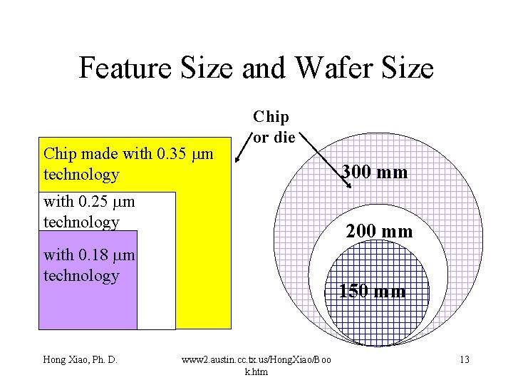
Feature Size and Wafer Size Chip made with 0. 35 mm technology Chip or die with 0. 25 mm technology 200 mm with 0. 18 mm technology Hong Xiao, Ph. D. 300 mm 150 mm www 2. austin. cc. tx. us/Hong. Xiao/Boo k. htm 13

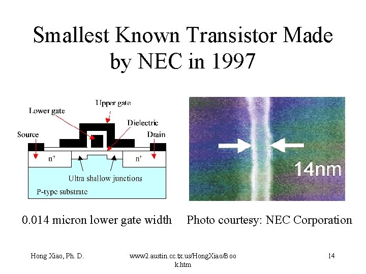
Smallest Known Transistor Made by NEC in 1997 0. 014 micron lower gate width Hong Xiao, Ph. D. Photo courtesy: NEC Corporation www 2. austin. cc. tx. us/Hong. Xiao/Boo k. htm 14

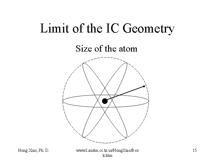
Limit of the IC Geometry Size of the atom Hong Xiao, Ph. D. www 2. austin. cc. tx. us/Hong. Xiao/Boo k. htm 15

Limit of the IC device • Atom size: several Å • Need some atoms to form a device • Likely the final limit is around 100 Å or 0. 01 micron. • About 30 silicon atoms Hong Xiao, Ph. D. www 2. austin. cc. tx. us/Hong. Xiao/Boo k. htm 16

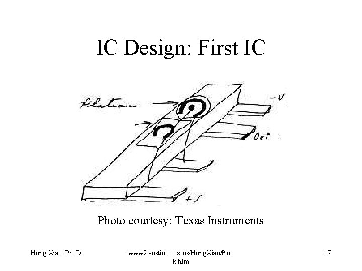
IC Design: First IC Photo courtesy: Texas Instruments Hong Xiao, Ph. D. www 2. austin. cc. tx. us/Hong. Xiao/Boo k. htm 17

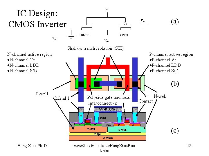
Vin IC Design: CMOS Inverter (a) Vdd NMOS Vss PMOS Vout Shallow trench isolation (STI) N-channel active region ·N-channel Vt ·N-channel LDD ·N-channel S/D P-channel active region ·P-channel Vt ·P-channel LDD ·P-channel S/D (b) P-well Polycide gate and local interconnection Metal 1 Contact N-well Metal 1, Al. Cu W n+ PMD n+ STI P-Well p+ p+ N-Well P-Epi (c) P-Wafer Hong Xiao, Ph. D. www 2. austin. cc. tx. us/Hong. Xiao/Boo k. htm 18

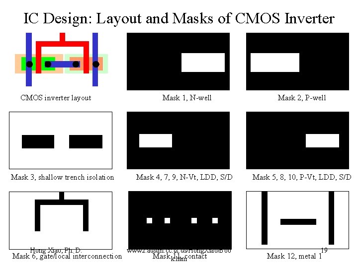
IC Design: Layout and Masks of CMOS Inverter CMOS inverter layout Mask 3, shallow trench isolation Hong Xiao, Ph. D. Mask 6, gate/local interconnection Mask 1, N-well Mask 4, 7, 9, N-Vt, LDD, S/D www 2. austin. cc. tx. us/Hong. Xiao/Boo Mask k. htm 11, contact Mask 2, P-well Mask 5, 8, 10, P-Vt, LDD, S/D 19 Mask 12, metal 1

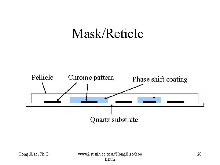
Mask/Reticle Pellicle Chrome pattern Phase shift coating Quartz substrate Hong Xiao, Ph. D. www 2. austin. cc. tx. us/Hong. Xiao/Boo k. htm 20

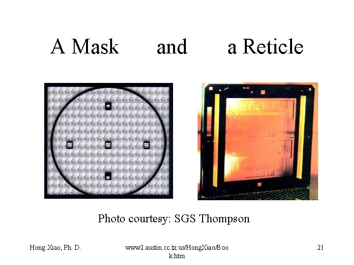
A Mask and a Reticle Photo courtesy: SGS Thompson Hong Xiao, Ph. D. www 2. austin. cc. tx. us/Hong. Xiao/Boo k. htm 21

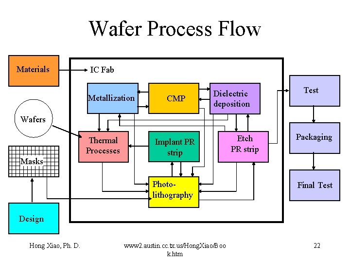
Wafer Process Flow Materials IC Fab Metallization CMP Dielectric deposition Test Wafers Thermal Processes Masks Implant PR strip Photolithography Etch PR strip Packaging Final Test Design Hong Xiao, Ph. D. www 2. austin. cc. tx. us/Hong. Xiao/Boo k. htm 22