Leakage in MOS devices Mohammad Sharifkhani Reading Text

- Slides: 25

Leakage in MOS devices Mohammad Sharifkhani

Reading • Text book, Chapter III • K. Roy’s Proc. of IEEE paper

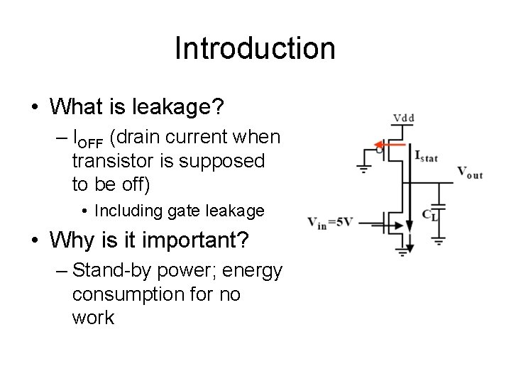
Introduction • What is leakage? – IOFF (drain current when transistor is supposed to be off) • Including gate leakage • Why is it important? – Stand-by power; energy consumption for no work

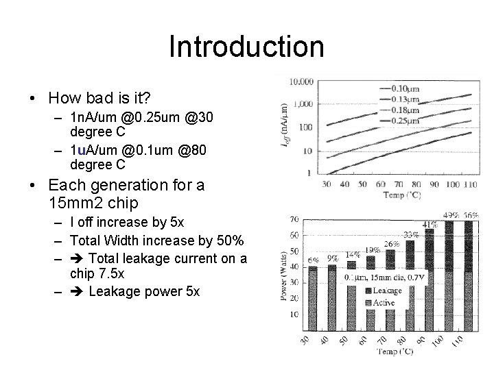
Introduction • How bad is it? – 1 n. A/um @0. 25 um @30 degree C – 1 u. A/um @0. 1 um @80 degree C • Each generation for a 15 mm 2 chip – I off increase by 5 x – Total Width increase by 50% – Total leakage current on a chip 7. 5 x – Leakage power 5 x

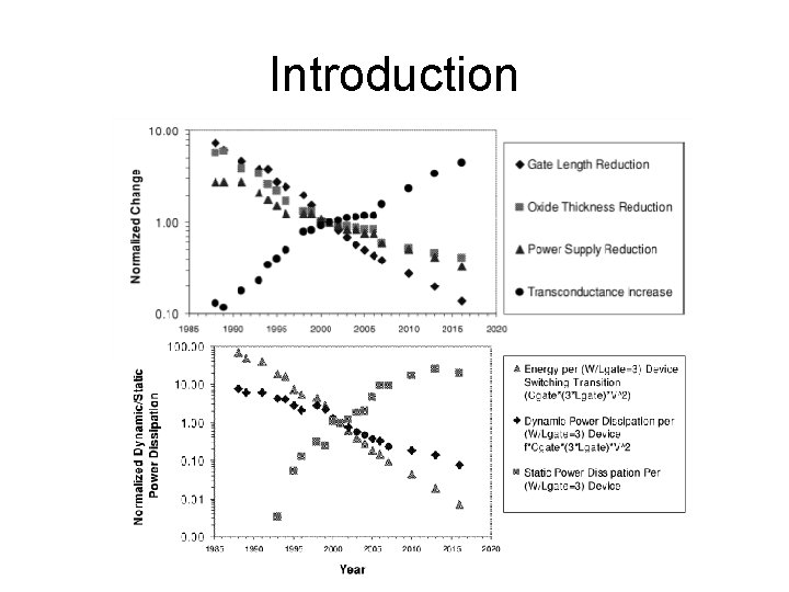
Introduction

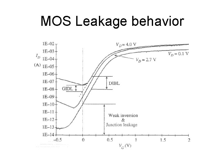
MOS Leakage behavior

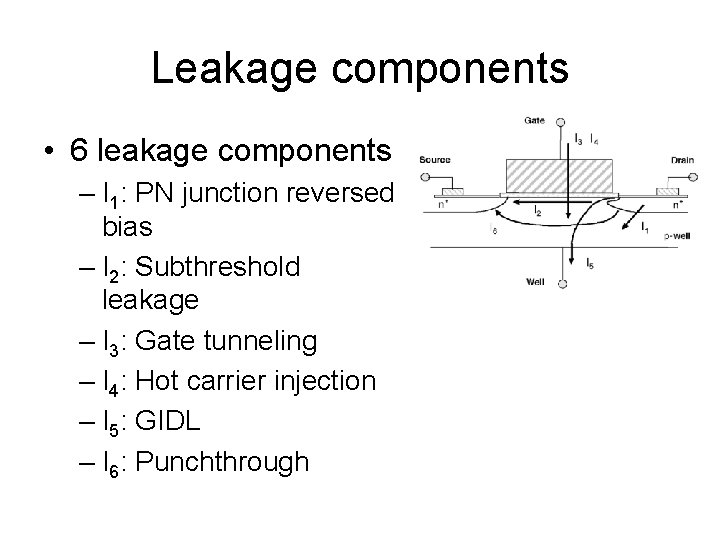
Leakage components • 6 leakage components – I 1: PN junction reversed bias – I 2: Subthreshold leakage – I 3: Gate tunneling – I 4: Hot carrier injection – I 5: GIDL – I 6: Punchthrough

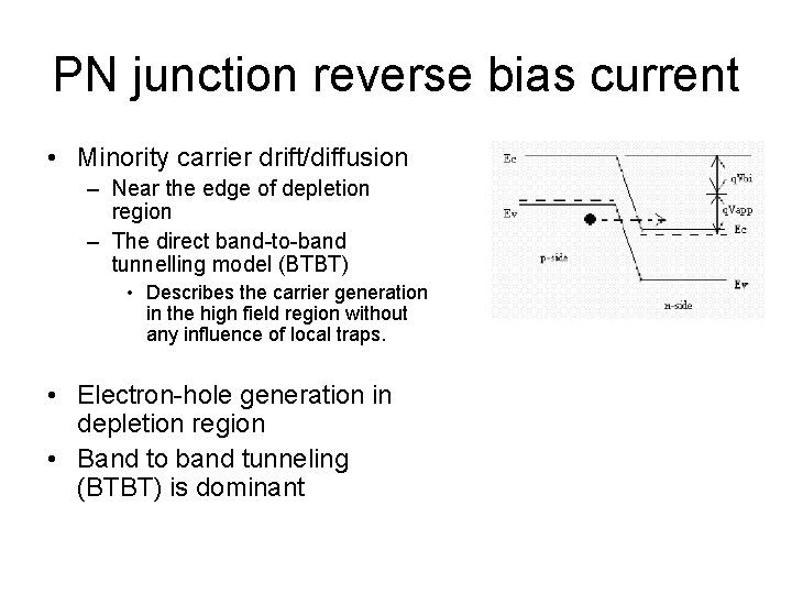
PN junction reverse bias current • Minority carrier drift/diffusion – Near the edge of depletion region – The direct band-to-band tunnelling model (BTBT) • Describes the carrier generation in the high field region without any influence of local traps. • Electron-hole generation in depletion region • Band to band tunneling (BTBT) is dominant

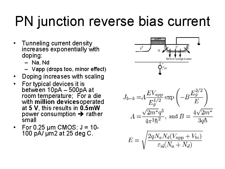
PN junction reverse bias current • Tunneling current density increases exponentially with doping: – Na, Nd – Vapp (drops too, minor effect) • Doping increases with scaling • For typical devices it is between 10 p. A – 500 p. A at room temperature; For a die with million devicesoperated at 5 V, this results in 0. 5 m. W power consumption rather small • For 0. 25 μm CMOS: J = 10100 p. A/ μm 2 at 25 deg C.

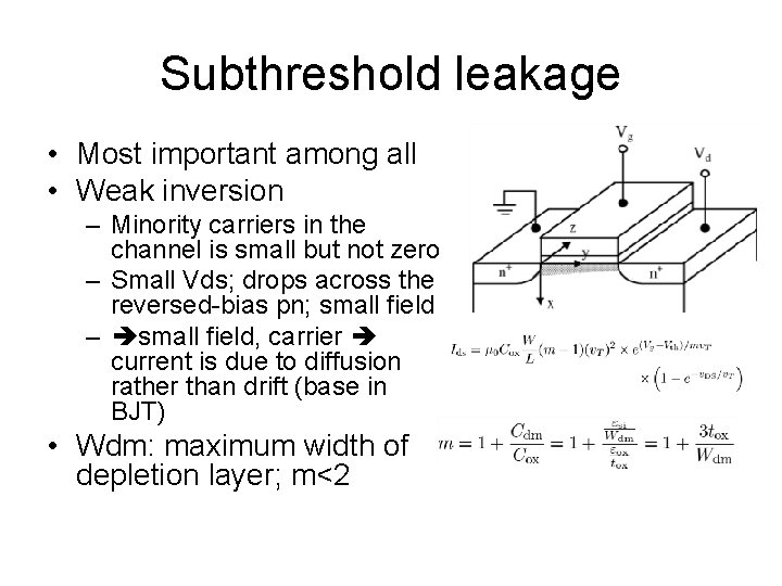
Subthreshold leakage • Most important among all • Weak inversion – Minority carriers in the channel is small but not zero – Small Vds; drops across the reversed-bias pn; small field – small field, carrier current is due to diffusion rather than drift (base in BJT) • Wdm: maximum width of depletion layer; m<2

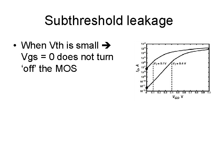
Subthreshold leakage • When Vth is small Vgs = 0 does not turn ‘off’ the MOS

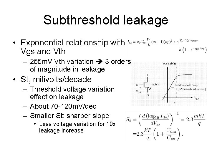
Subthreshold leakage • Exponential relationship with Vgs and Vth – 255 m. V Vth variation 3 orders of magnitude in leakage • St; milivolts/decade – Threshold voltage variation effect on leakage – About 70 -120 m. V/dec – Smaller St: sharper slope • Less voltage variation for 10 x leakage increase

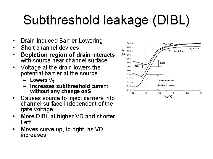
Subthreshold leakage (DIBL) • Drain Induced Barrier Lowering • Short channel devices • Depletion region of drain interacts with source near channel surface • Voltage at the drain lowers the potential barrier at the source – Lowers VTh – Increases subthreshold current without any change on. S • Causes source to inject carriers into channel surface independent of the gate voltage • More DIBL at higher VD and shorter Leff • Moves curve up, to right, as VD increases

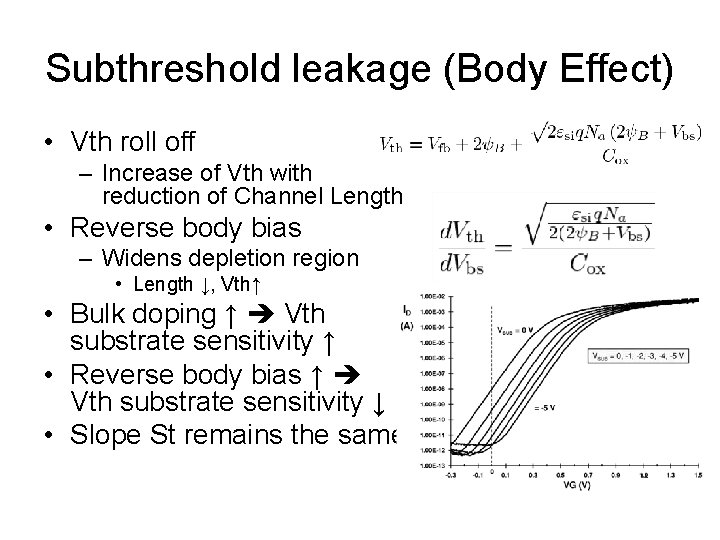
Subthreshold leakage (Body Effect) • Vth roll off – Increase of Vth with reduction of Channel Length • Reverse body bias – Widens depletion region • Length ↓, Vth↑ • Bulk doping ↑ Vth substrate sensitivity ↑ • Reverse body bias ↑ Vth substrate sensitivity ↓ • Slope St remains the same

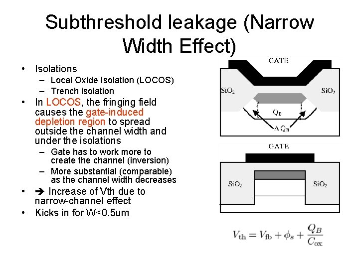
Subthreshold leakage (Narrow Width Effect) • Isolations – Local Oxide Isolation (LOCOS) – Trench isolation • In LOCOS, the fringing field causes the gate-induced depletion region to spread outside the channel width and under the isolations – Gate has to work more to create the channel (inversion) – More substantial (comparable) as the channel width decreases • Increase of Vth due to narrow-channel effect • Kicks in for W<0. 5 um

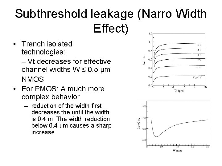
Subthreshold leakage (Narro Width Effect) • Trench isolated technologies: – Vt decreases for effective channel widths W ≤ 0. 5 μm NMOS • For PMOS: A much more complex behavior – reduction of the width first decreases the until the width is 0. 4 m. The width reduction below 0. 4 um causes a sharp increase

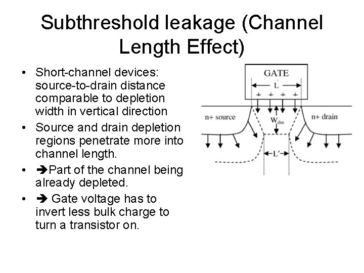
Subthreshold leakage (Channel Length Effect) • Short-channel devices: source-to-drain distance comparable to depletion width in vertical direction • Source and drain depletion regions penetrate more into channel length. • Part of the channel being already depleted. • Gate voltage has to invert less bulk charge to turn a transistor on.

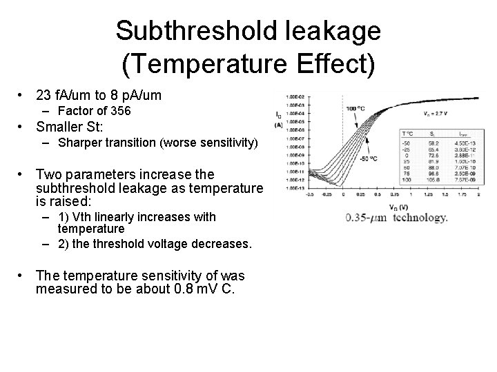
Subthreshold leakage (Temperature Effect) • 23 f. A/um to 8 p. A/um – Factor of 356 • Smaller St: – Sharper transition (worse sensitivity) • Two parameters increase the subthreshold leakage as temperature is raised: – 1) Vth linearly increases with temperature – 2) the threshold voltage decreases. • The temperature sensitivity of was measured to be about 0. 8 m. V C.

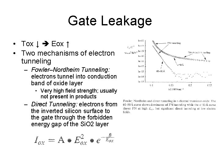
Gate Leakage • Tox ↓ Eox ↑ • Two mechanisms of electron tunneling – Fowler–Nordheim Tunneling: electrons tunnel into conduction band of oxide layer • Very high field strength; usually not present in products – Direct Tunneling: electrons from the inverted silicon surface to the gate through the forbidden energy gap of the Si. O 2 layer

Hot Carrier Injection • In a short-channel transistor, due to high electric field near the Si–Si. O 2 interface, electrons or holes can gain sufficient energy from the electric field to cross the interface potential barrier and enter into the oxide layer – Reliability risk! (Electrons can trap into or destroy oxide) • Increases as L drops (unless VDD drops accordingly)

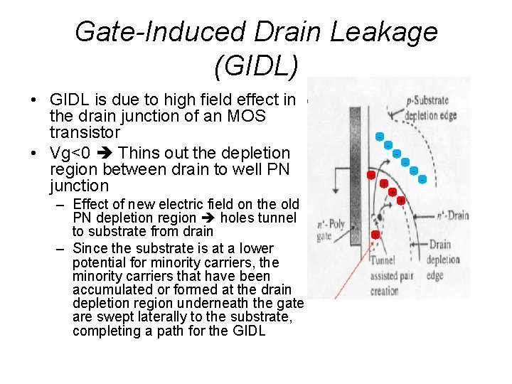
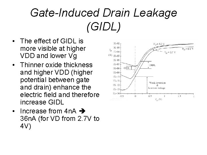
Gate-Induced Drain Leakage (GIDL) • GIDL is due to high field effect in the drain junction of an MOS transistor • Vg<0 Thins out the depletion region between drain to well PN junction – Effect of new electric field on the old PN depletion region holes tunnel to substrate from drain – Since the substrate is at a lower potential for minority carriers, the minority carriers that have been accumulated or formed at the drain depletion region underneath the gate are swept laterally to the substrate, completing a path for the GIDL - + + - + - -

Gate-Induced Drain Leakage (GIDL) • The effect of GIDL is more visible at higher VDD and lower Vg • Thinner oxide thickness and higher VDD (higher potential between gate and drain) enhance the electric field and therefore increase GIDL • Increase from 4 n. A 36 n. A (for VD from 2. 7 V to 4 V)

Gate-Induced Drain Leakage (GIDL) • • Increasing current for negative VG values • Localized along channel width between gate and drain • Major problem in Ioff current: • Contributes to standby power, so must control this by increasing oxide thickness, increasing drain doping, or eliminating traps. • For high performance device (low Vth), is not a major issue.

Punchthrough • When Source and Drain depletion region “touch” each other deep in the channel. • Less gate influence on the current – Channel is created deeper in substrate – Higher St • Varies quadratically with VD and with VS

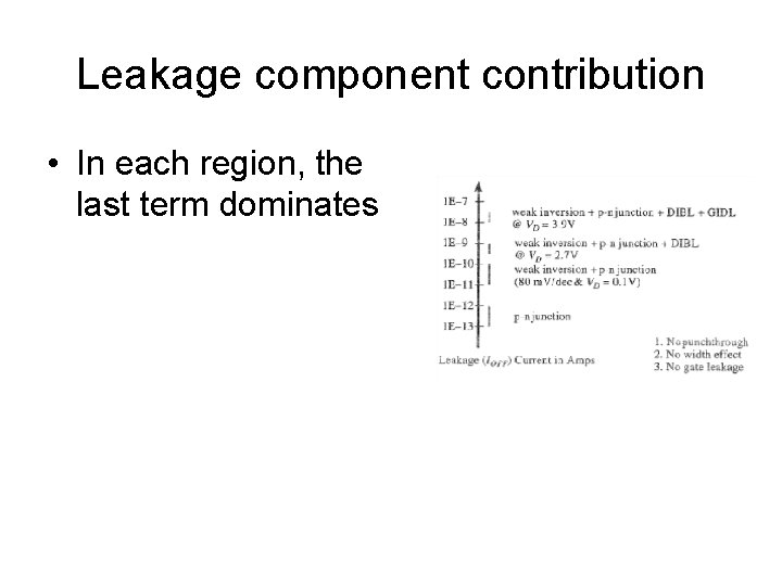
Leakage component contribution • In each region, the last term dominates