INTRODUCTION TO HIGHDENSITY INTERCONNECTION TECHNOLOGIES ON SILICON WAFERS




- Slides: 46

INTRODUCTION TO HIGH-DENSITY INTERCONNECTION TECHNOLOGIES ON SILICON WAFERS ESE SEMINAR 12 -JANUARY-2010 SAMI VAEHAENEN – CERN PH-ESE 1

Brief Introduction to author’s Work at CERN • White paper study on low-cost bump bonding solutions. • Present day bump bonding services for pixel detectors are very expensive on assembly level. • To cover larger areas with pixel detectors in LHC upgrade, reliable bump bonding services must cheaper. • Identifying and testing of methods providing cost-savings in fine-pitch bump bonding. • Finding optimal process windows to optimize cost structure. • Studying 3 D integration and benchmarking of industrial manufacturing techniques (this presentation). • Participating in TSV process development with collaborating institute. 2

Outline • Introduction • Flip chip bonding • Advanced wafer-level packaging techniques • SLID soldering • Chip-to-wafer-bonding • Wafer-to-wafer bonding • Through silicon vias (TSV) • 3 D integration roadmaps • 3 D integrated device example • Summary 3

Introduction • Presentation aims at giving a brief overall view of the present day and near-future packaging technologies for silicon substrates. • Pixel detectors are used as reference with various technologies. • Technologies will be likely be applied to SLHC upgrade. • Packaging industry is under revolution because of the transistor scaling era is ending and 3 D integration era with through silicon vias (TSV) is beginning. • TSV processes have a major impact on development of: • Ultra-high density interconnection methods • Process equipments • Bump sizes and pitches in the commercial electronics. • Thinning and handling of wafers 4

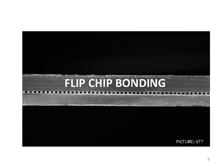
FLIP CHIP BONDING PICTURE: VTT 5

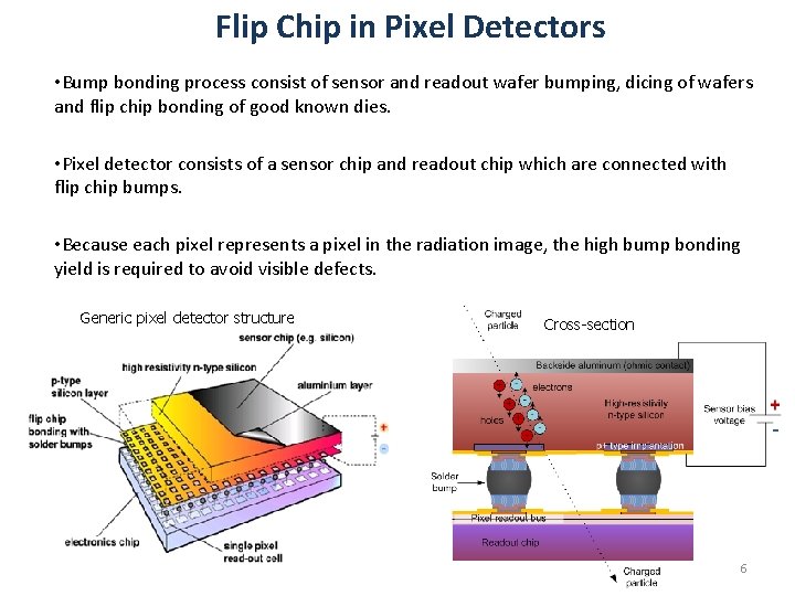
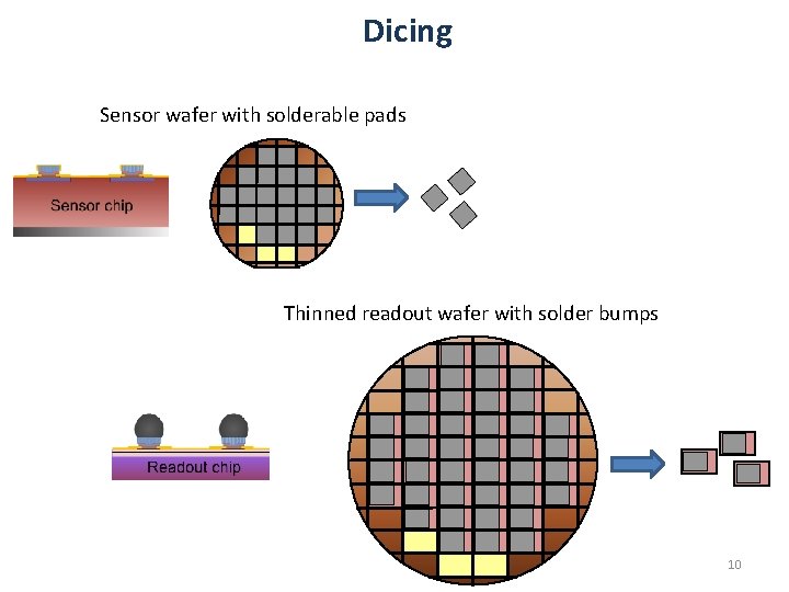
Flip Chip in Pixel Detectors • Bump bonding process consist of sensor and readout wafer bumping, dicing of wafers and flip chip bonding of good known dies. • Pixel detector consists of a sensor chip and readout chip which are connected with flip chip bumps. • Because each pixel represents a pixel in the radiation image, the high bump bonding yield is required to avoid visible defects. Generic pixel detector structure Cross-section 6

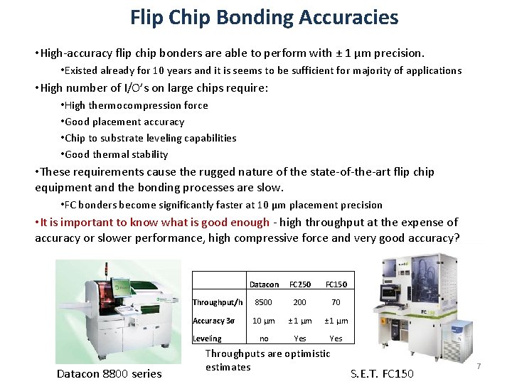
Flip Chip Bonding Accuracies • High-accuracy flip chip bonders are able to perform with ± 1 µm precision. • Existed already for 10 years and it is seems to be sufficient for majority of applications • High number of I/O’s on large chips require: • High thermocompression force • Good placement accuracy • Chip to substrate leveling capabilities • Good thermal stability • These requirements cause the rugged nature of the state-of-the-art flip chip equipment and the bonding processes are slow. • FC bonders become significantly faster at 10 µm placement precision • It is important to know what is good enough - high throughput at the expense of accuracy or slower performance, high compressive force and very good accuracy? Datacon FC 250 FC 150 Throughput/h 8500 200 70 Accuracy 3σ 10 µm ± 1 µm no Yes Leveling Datacon 8800 series Throughputs are optimistic estimates S. E. T. FC 150 7

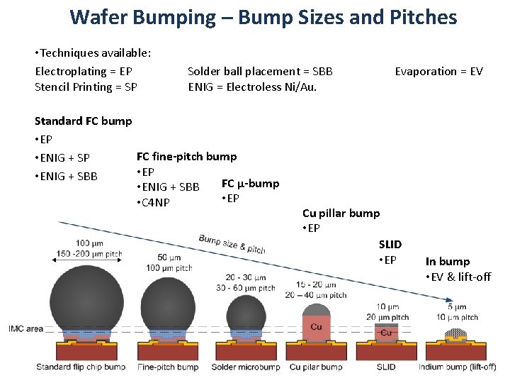
Wafer Bumping – Bump Sizes and Pitches • Techniques available: Electroplating = EP Stencil Printing = SP Solder ball placement = SBB ENIG = Electroless Ni/Au. Standard FC bump • EP FC fine-pitch bump • ENIG + SP • ENIG + SBB FC µ-bump • ENIG + SBB • EP • C 4 NP Evaporation = EV Cu pillar bump • EP SLID • EP In bump • EV & lift-off

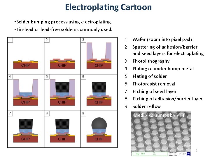
Electroplating Cartoon • Solder bumping process using electroplating. • Tin-lead or lead-free solders commonly used. 1. Wafer (zoom into pixel pad) 2. Sputtering of adhesion/barrier and seed layers for electroplating 3. Photolithography 4. Plating of under bump metal 5. Plating of solder 6. Photoresist removal 7. Etching of seed layer 8. Etching of adhesion/barrier layer 9. Solder reflow Medipix 2 bumps by VTT 9

Dicing Sensor wafer with solderable pads Thinned readout wafer with solder bumps 10

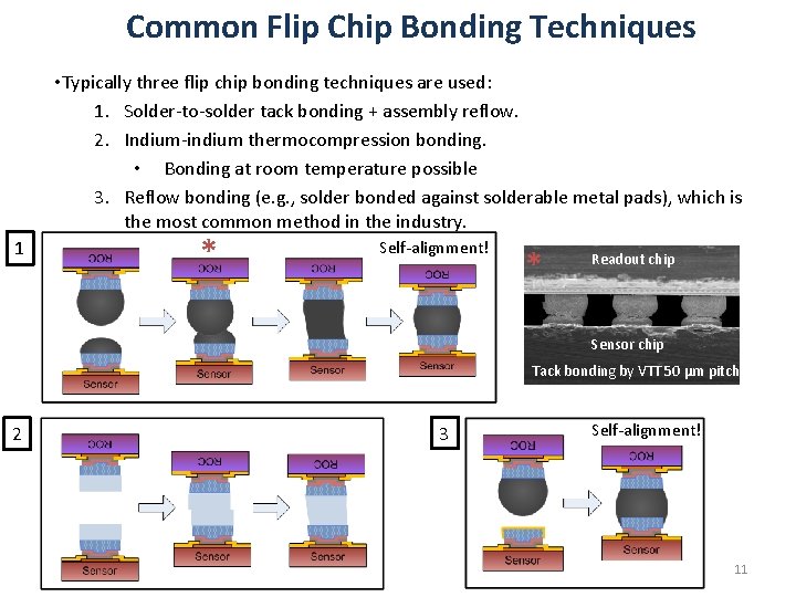
Common Flip Chip Bonding Techniques • Typically three flip chip bonding techniques are used: 1. Solder-to-solder tack bonding + assembly reflow. 2. Indium-indium thermocompression bonding. • Bonding at room temperature possible 3. Reflow bonding (e. g. , solder bonded against solderable metal pads), which is the most common method in the industry. 1 * Self-alignment! * Readout chip Sensor chip Tack bonding by VTT 50 µm pitch 2 3 Self-alignment! 11

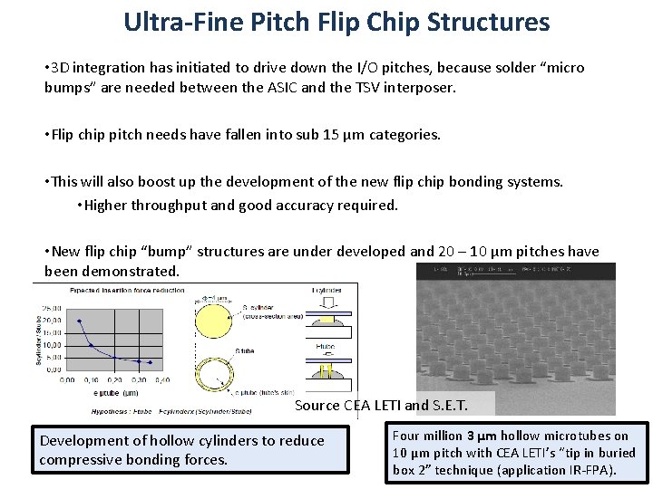
Ultra-Fine Pitch Flip Chip Structures • 3 D integration has initiated to drive down the I/O pitches, because solder “micro bumps” are needed between the ASIC and the TSV interposer. • Flip chip pitch needs have fallen into sub 15 µm categories. • This will also boost up the development of the new flip chip bonding systems. • Higher throughput and good accuracy required. • New flip chip “bump” structures are under developed and 20 – 10 µm pitches have been demonstrated. Source CEA LETI and S. E. T. Development of hollow cylinders to reduce compressive bonding forces. Four million 3 µm hollow microtubes on 10 µm pitch with CEA LETI’s “tip in buried box 2” technique (application IR-FPA).

ADVANCED WAFER-LEVEL PACKAGING TECHNIQUES 13

Advanced High-Density Interconnection Methods • Chip-to-chip (C 2 C) bonding is mostly used in assembly of pixel detectors at the moment, but focus is being moved to wafer-scale processes. • Emerging bonding solutions are: • Solid-Liquid-Inter-Diffusion (SLID) soldering • Chip-to-wafer bonding (C 2 W) – chips are bonded on a wafer in sequence • Wafer-to-wafer bonding (W 2 W) • Through silicon vias will revolutionize the I/O densities in packages. • Carbon nanotubes are left outside this presentation. • C 2 W bonding will increase throughput in flip chip assembly by reducing process steps. • Individual good known dies (KGD) are flip chip bonded on KGD’s on the wafer in sequence. • Increased throughput compared to C 2 C bonding and easier handling of assemblies. • W 2 W bonding, the ultimate assembly method • High throughput and very good bonding accuracy • Many restrictions 14

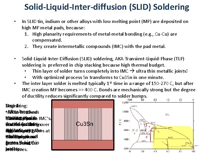
Solid-Liquid-Inter-diffusion (SLID) Soldering • In SLID tin, indium or other alloys with low melting point (MP) are deposited on high MP metal pads, because: 1. High planarity requirements of metal-metal bonding (e. g. , Cu-Cu) are compensated. 2. They create intermetallic compounds (IMC) with the pad metal. • Solid-Liquid-Inter-Diffusion (SLID) soldering, AKA Transient-Liquid-Phase (TLP) soldering is preferred in chip stacking because high thermal budget. • Thin layer of solder turns completely into IMC ultra thin metallic joints! • With optimized process Sn transforms to Cu 3 Sn in one minute. The inter layer solder is melted typically 1 st time in a range of 150 -270 C, but after IMC creation MP becomes >> 400 C. Bonds are mechanically strong but the degree of ductility reduces significantly compared to solder bumps. • Step 4: Step 1 Beginning: Step 2: Step 3: • After long Cross-hatched All Sn has been heating, the • Thick Cu pads Sn reacts with Cu 6 Sn 5 phase transformed to IMC’s. ductile Cu 3 Sn Cu and creates and < 5 µm of Sn. • consumes the Sn Cu 3 Sn is taking over expands over the • IMC’s. aggressively. Cu 6 Sn 5 and grows at Bonding at 270 – whole area and Cu 6 Sn 5 phase • 300 the expense of Cu 3 Sn phase C. forms the a thin grows in big grows on at Cu Cu 6 Sn 5 and Cu. joint. scallops. interfaces. 15

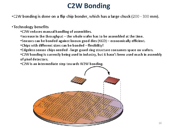
C 2 W Bonding • C 2 W bonding is done on a flip chip bonder, which has a large chuck (200 - 300 mm). • Technology benefits • C 2 W reduces manual handling of assemblies. • Increase in the throughput – the whole wafer has to be assembled at the time. • Sensors can be bonded against known good dies (KGD) – economically efficient. • Chips with different sizes can be bonded – flexibility! • Edgeless sensor chips needed - large guard ring structure consumes space on wafers. • C 2 W bonding is currently being used in industry, but it hasn’t been used much in assembly of pixel detectors. • C 2 W is an intermediate step towards W 2 W bonding. 16

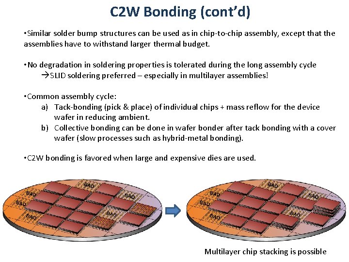
C 2 W Bonding (cont’d) • Similar solder bump structures can be used as in chip-to-chip assembly, except that the assemblies have to withstand larger thermal budget. • No degradation in soldering properties is tolerated during the long assembly cycle SLID soldering preferred – especially in multilayer assemblies! • Common assembly cycle: a) Tack-bonding (pick & place) of individual chips + mass reflow for the device wafer in reducing ambient. b) Collective bonding can be done in wafer bonder after tack bonding with a cover wafer (slow processes such as hybrid-metal bonding). • C 2 W bonding is favored when large and expensive dies are used. Multilayer chip stacking is possible

W 2 W Bonding - Introduction • Wafer bonders are basically modified mask aligners and have an excellent accuracy (sub 1 µm). • Wafer bonder which is equipped with 2 -side heating, force loading and vacuum & reactive gas or ion milling chamber is capable for various assembly processes. • Direct bonding of wafers is generally based on bringing well polished wafers together • Surface roughness in Angstrom (0. 1 nm) scale required. • W 2 W techniques for bonding 3 D integrated already wafers exist, but they still need some optimization. • There is a big variety of bonding materials for making ultra thin interconnections. • Cu-Cu, solder-solder, Au-Au, metal-polymer hybrid bonding, oxide-oxide, DBI bonding (Ziptronix), SLID etc. 18

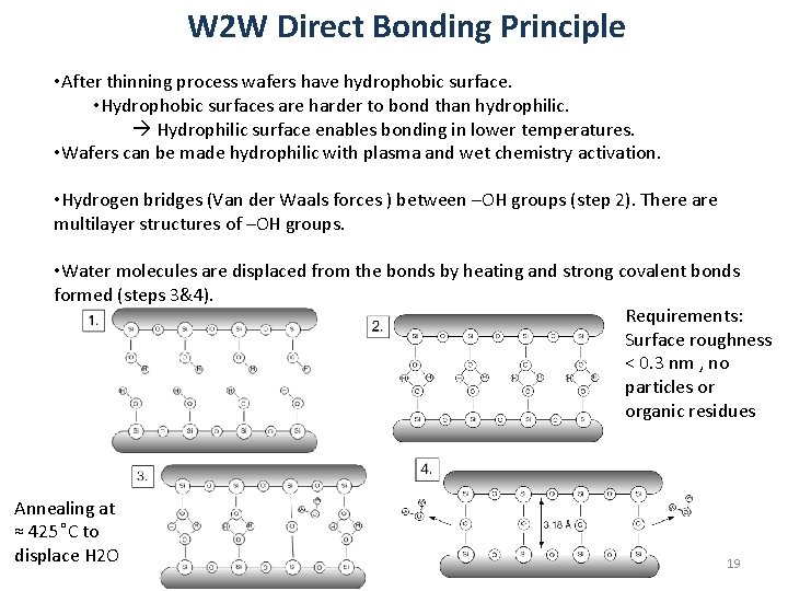
W 2 W Direct Bonding Principle • After thinning process wafers have hydrophobic surface. • Hydrophobic surfaces are harder to bond than hydrophilic. Hydrophilic surface enables bonding in lower temperatures. • Wafers can be made hydrophilic with plasma and wet chemistry activation. • Hydrogen bridges (Van der Waals forces ) between –OH groups (step 2). There are multilayer structures of –OH groups. • Water molecules are displaced from the bonds by heating and strong covalent bonds formed (steps 3&4). Requirements: Surface roughness < 0. 3 nm , no particles or organic residues Annealing at ≈ 425 C to displace H 2 O 19

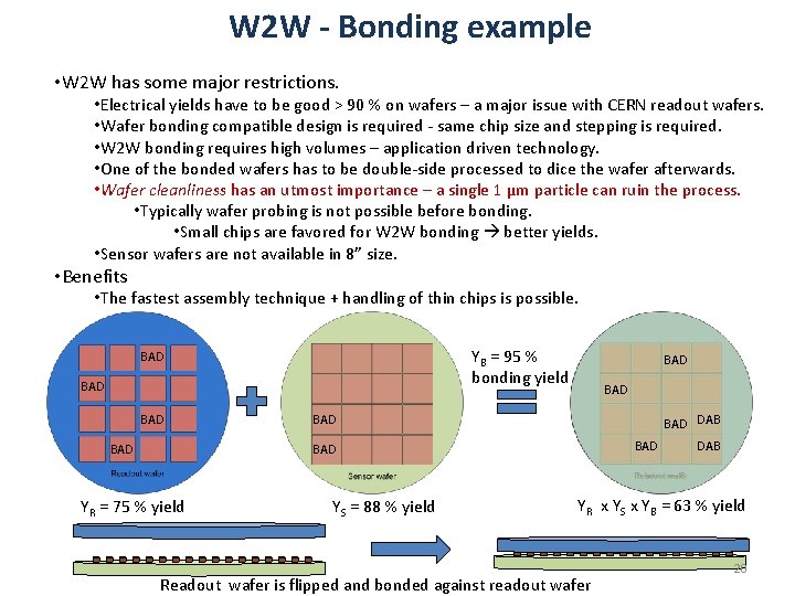
W 2 W - Bonding example • W 2 W has some major restrictions. • Electrical yields have to be good > 90 % on wafers – a major issue with CERN readout wafers. • Wafer bonding compatible design is required - same chip size and stepping is required. • W 2 W bonding requires high volumes – application driven technology. • One of the bonded wafers has to be double-side processed to dice the wafer afterwards. • Wafer cleanliness has an utmost importance – a single 1 µm particle can ruin the process. • Typically wafer probing is not possible before bonding. • Small chips are favored for W 2 W bonding better yields. • Sensor wafers are not available in 8” size. • Benefits • The fastest assembly technique + handling of thin chips is possible. YB = 95 % bonding yield BAD BAD DAB BAD YR = 75 % yield YS = 88 % yield DAB YR x YS x YB = 63 % yield Readout wafer is flipped and bonded against readout wafer 20

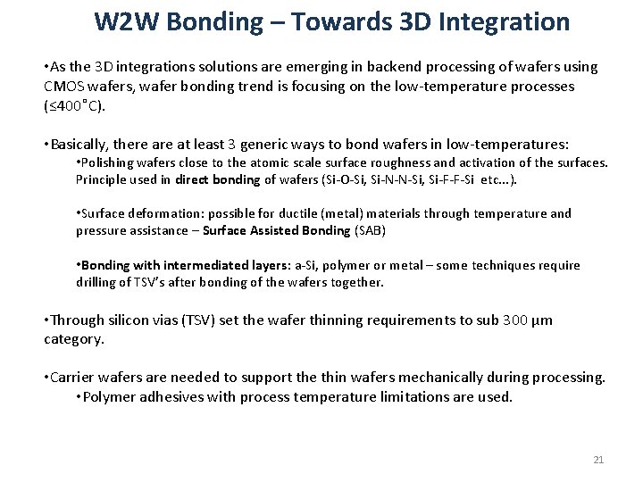
W 2 W Bonding – Towards 3 D Integration • As the 3 D integrations solutions are emerging in backend processing of wafers using CMOS wafers, wafer bonding trend is focusing on the low-temperature processes (≤ 400 C). • Basically, there at least 3 generic ways to bond wafers in low-temperatures: • Polishing wafers close to the atomic scale surface roughness and activation of the surfaces. Principle used in direct bonding of wafers (Si-O-Si, Si-N-N-Si, Si-F-F-Si etc. . . ). • Surface deformation: possible for ductile (metal) materials through temperature and pressure assistance – Surface Assisted Bonding (SAB) • Bonding with intermediated layers: a-Si, polymer or metal – some techniques require drilling of TSV’s after bonding of the wafers together. • Through silicon vias (TSV) set the wafer thinning requirements to sub 300 µm category. • Carrier wafers are needed to support the thin wafers mechanically during processing. • Polymer adhesives with process temperature limitations are used. 21

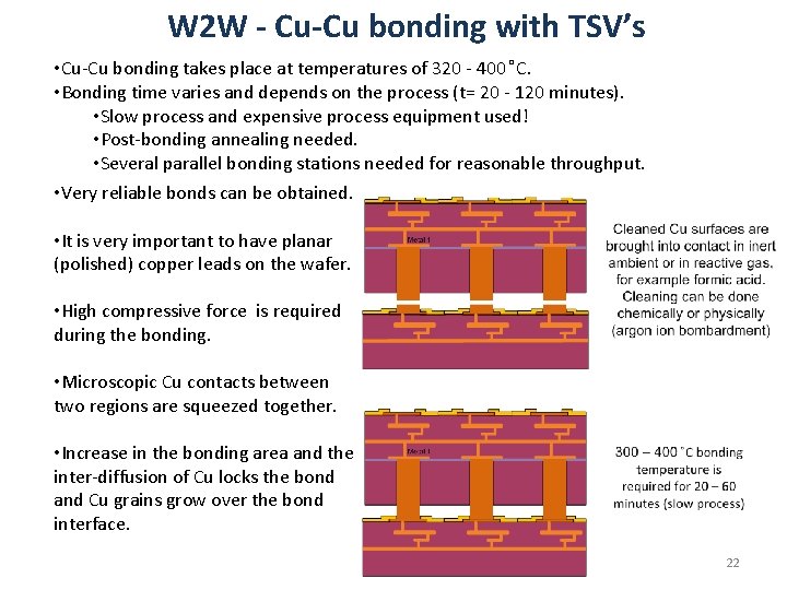
W 2 W - Cu-Cu bonding with TSV’s • Cu-Cu bonding takes place at temperatures of 320 - 400 C. • Bonding time varies and depends on the process (t= 20 - 120 minutes). • Slow process and expensive process equipment used! • Post-bonding annealing needed. • Several parallel bonding stations needed for reasonable throughput. • Very reliable bonds can be obtained. • It is very important to have planar (polished) copper leads on the wafer. • High compressive force is required during the bonding. • Microscopic Cu contacts between two regions are squeezed together. • Increase in the bonding area and the inter-diffusion of Cu locks the bond and Cu grains grow over the bond interface. 22

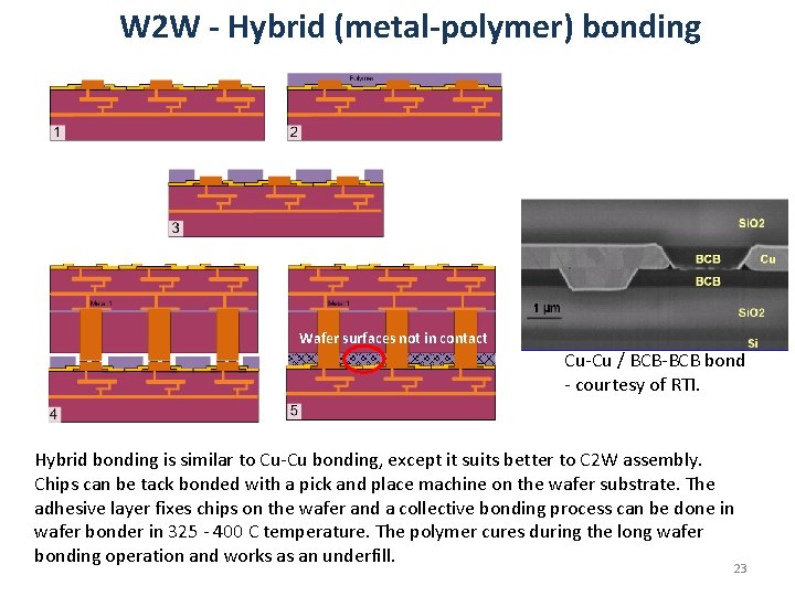
W 2 W - Hybrid (metal-polymer) bonding Wafer surfaces not in contact Cu-Cu / BCB-BCB bond - courtesy of RTI. Hybrid bonding is similar to Cu-Cu bonding, except it suits better to C 2 W assembly. Chips can be tack bonded with a pick and place machine on the wafer substrate. The adhesive layer fixes chips on the wafer and a collective bonding process can be done in wafer bonder in 325 - 400 C temperature. The polymer cures during the long wafer bonding operation and works as an underfill. 23

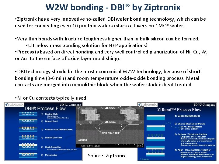
W 2 W bonding - DBI® by Ziptronix • Ziptronix has a very innovative so-called DBI wafer bonding technology, which can be used for connecting even 10 µm thin wafers (stack of layers on CMOS wafer). • Very thin bonds with fracture toughness higher than in bulk silicon can be formed. • Ultra-low mass bonding solution for HEP applications! • Process is based on direct bonding and very well controlled planarization of Ni, Cu, W, or Au to the surface of oxide layer (no dishing). • DBI technology should be the most economical W 2 W technology, because of short bonding time (3 -6 min) and room temperature oxide-oxide bonding process. Metal contacts are merged into monolithic block when the wafer stack is heat treated. • Ni or Cu contacts typically used. Source: Ziptronix

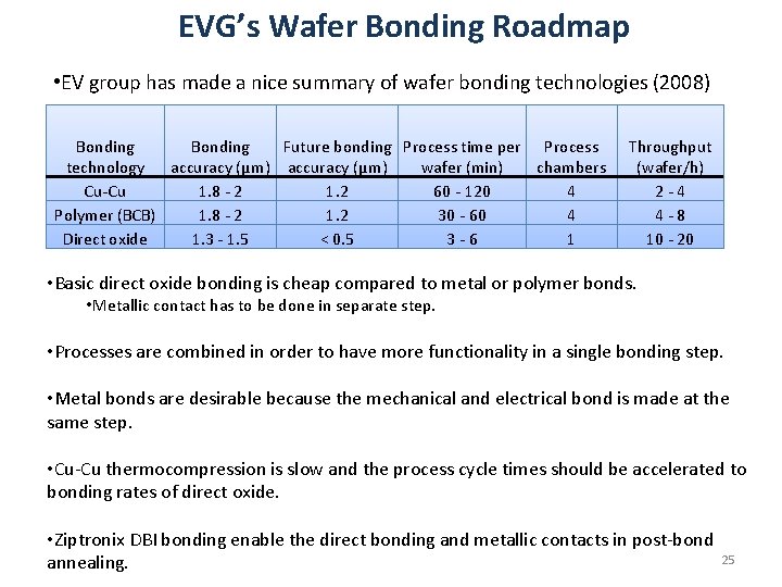
EVG’s Wafer Bonding Roadmap • EV group has made a nice summary of wafer bonding technologies (2008) Bonding Future bonding Process time per Process technology accuracy (µm) wafer (min) chambers Cu-Cu 1. 8 - 2 1. 2 60 - 120 4 Polymer (BCB) 1. 8 - 2 1. 2 30 - 60 4 Direct oxide 1. 3 - 1. 5 < 0. 5 3 - 6 1 Throughput (wafer/h) 2 - 4 4 - 8 10 - 20 • Basic direct oxide bonding is cheap compared to metal or polymer bonds. • Metallic contact has to be done in separate step. • Processes are combined in order to have more functionality in a single bonding step. • Metal bonds are desirable because the mechanical and electrical bond is made at the same step. • Cu-Cu thermocompression is slow and the process cycle times should be accelerated to bonding rates of direct oxide. • Ziptronix DBI bonding enable the direct bonding and metallic contacts in post-bond 25 annealing.

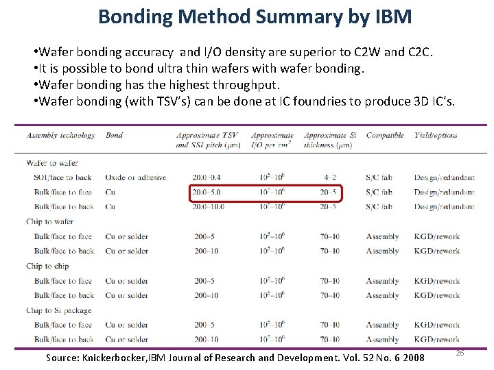
Bonding Method Summary by IBM • Wafer bonding accuracy and I/O density are superior to C 2 W and C 2 C. • It is possible to bond ultra thin wafers with wafer bonding. • Wafer bonding has the highest throughput. • Wafer bonding (with TSV’s) can be done at IC foundries to produce 3 D IC’s. Source: Knickerbocker, IBM Journal of Research and Development. Vol. 52 No. 6 2008 26

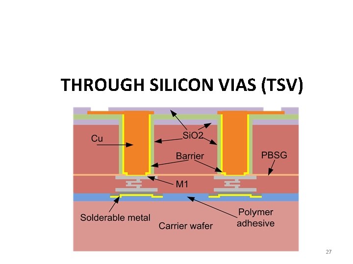
THROUGH SILICON VIAS (TSV) 27

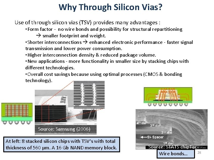
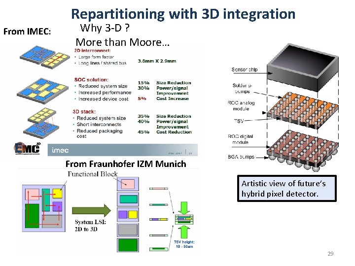
Why Through Silicon Vias? Use of through silicon vias (TSV) provides many advantages : • Form factor - no wire bonds and possibility for structural repartitioning smaller footprint and weight. • Shorter interconnections enhanced electronic performance - faster signal transmission and lower power consumption. • Higher interconnection density & reduced package volume. • New applications - more functionality in smaller size by stacking chips with different technologies. • Overall cost savings because using optimal processes (CMOS & bonding technology). Source: Samsung (2006) At left: 8 stacked silicon chips with TSV’s with total thickness of 560 µm. A 16 Gb NAND memory block. Source: STATS chip. Pac 28 Wire bonds…

Repartitioning with 3 D integration From IMEC: Why 3 -D ? More than Moore… From Fraunhofer IZM Munich Artistic view of future’s hybrid pixel detector. 29

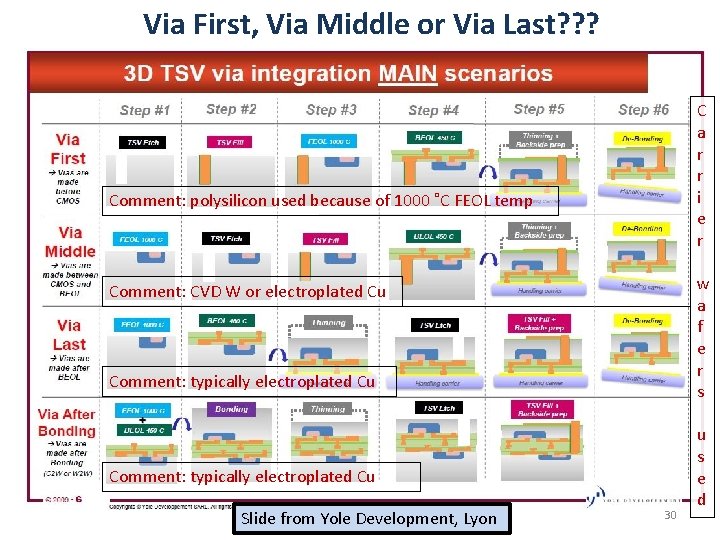
Via First, Via Middle or Via Last? ? ? C a r r i e r w a f e r s Comment: polysilicon used because of 1000 ˚C FEOL temp Comment: CVD W or electroplated Cu Comment: typically electroplated Cu Slide from Yole Development, Lyon 30 u s e d

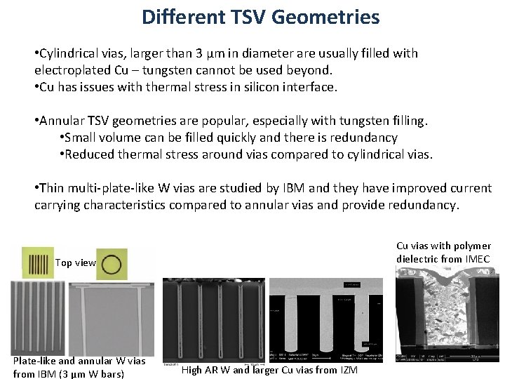
Different TSV Geometries • Cylindrical vias, larger than 3 µm in diameter are usually filled with electroplated Cu – tungsten cannot be used beyond. • Cu has issues with thermal stress in silicon interface. • Annular TSV geometries are popular, especially with tungsten filling. • Small volume can be filled quickly and there is redundancy • Reduced thermal stress around vias compared to cylindrical vias. • Thin multi-plate-like W vias are studied by IBM and they have improved current carrying characteristics compared to annular vias and provide redundancy. Cu vias with polymer dielectric from IMEC Top view Plate-like and annular W vias from IBM (3 µm W bars) High AR W and larger Cu vias from IZM

High-Energy Physics and TSV’s • TSV development work is done parallel with via middle and via last methods within CERN experiments. • Via last processes can be demonstrated with existing wafers if the designs are compatible with it. • Work done in European research companies IMEC and IZM are strong in via last TSV technology and they are close to produce the first TSV’s for CERN CMOS wafers. VTT is working on Medipix 3 wafers. • Via first/middle technologies would lead to ultimate goal (3 D IC), but is the technology available for small volume products? • 3 D IC consortium (many institutes in HEP field) using Chartered 0. 13 µm wafers and Tezzaron metallization and bonding processes. • Process run scheduled January-February time window. • After via middle TSV’s will be commercially available, the readout chip designs will go through a major change (signals taken out over the whole area – not only via chip perimeter) be prepared for this! 32

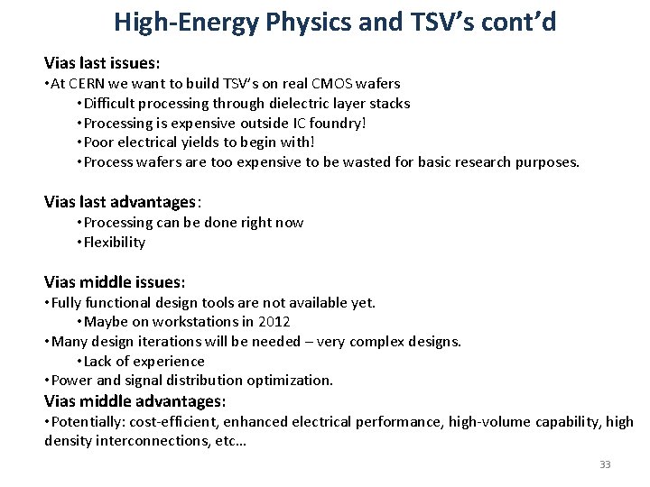
High-Energy Physics and TSV’s cont’d Vias last issues: • At CERN we want to build TSV’s on real CMOS wafers • Difficult processing through dielectric layer stacks • Processing is expensive outside IC foundry! • Poor electrical yields to begin with! • Process wafers are too expensive to be wasted for basic research purposes. Vias last advantages: • Processing can be done right now • Flexibility Vias middle issues: • Fully functional design tools are not available yet. • Maybe on workstations in 2012 • Many design iterations will be needed – very complex designs. • Lack of experience • Power and signal distribution optimization. Vias middle advantages: • Potentially: cost-efficient, enhanced electrical performance, high-volume capability, high density interconnections, etc… 33

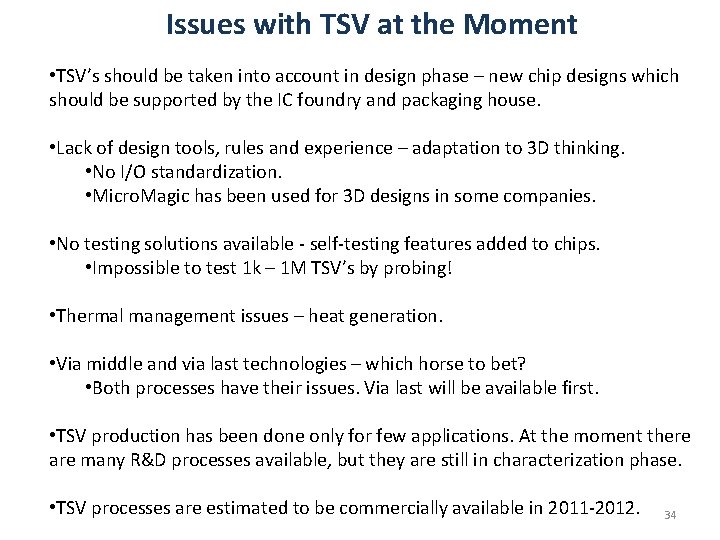
Issues with TSV at the Moment • TSV’s should be taken into account in design phase – new chip designs which should be supported by the IC foundry and packaging house. • Lack of design tools, rules and experience – adaptation to 3 D thinking. • No I/O standardization. • Micro. Magic has been used for 3 D designs in some companies. • No testing solutions available - self-testing features added to chips. • Impossible to test 1 k – 1 M TSV’s by probing! • Thermal management issues – heat generation. • Via middle and via last technologies – which horse to bet? • Both processes have their issues. Via last will be available first. • TSV production has been done only for few applications. At the moment there are many R&D processes available, but they are still in characterization phase. • TSV processes are estimated to be commercially available in 2011 -2012. 34

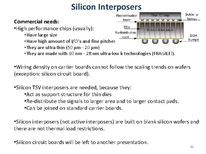
Silicon Interposers Commercial needs: • High performance chips (usually): • Have large size • Have high amount of I/O’s and fine pitches. • They are ultra thin (50 µm - 20 µm) • They are made with 90 nm - 28 nm ultra-low k technologies (FRAGILE!). • Wiring density on carrier boards cannot follow the scaling trends on wafers (exception: silicon circuit board). • Silicon TSV interposers are needed, because they: • Act as support structure for thin dies • Re-distribute the signals to larger area and to larger contact pads. • Can be joined on standard carrier boards. • Silicon interposers (not active interposers) are built on blank silicon wafers and there are not thermal load restrictions. • Silicon circuit boards will be left to another presentation. 35

3 D INTEGRATION ROADMAPS The Long road to TSV’s 36

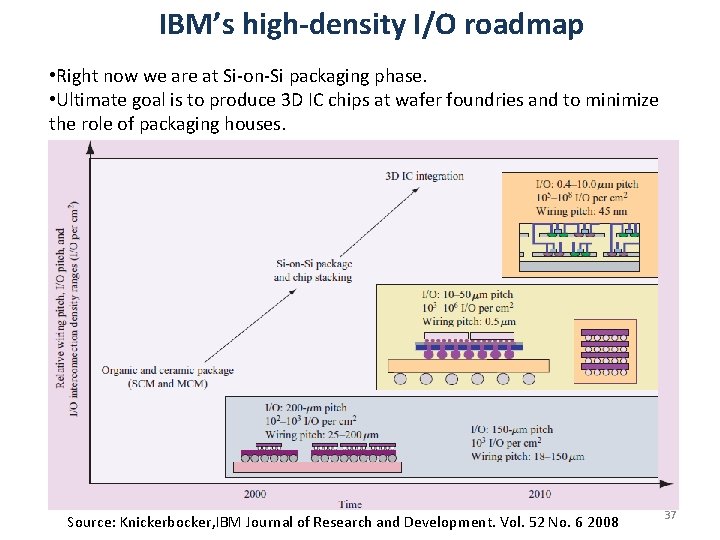
IBM’s high-density I/O roadmap • Right now we are at Si-on-Si packaging phase. • Ultimate goal is to produce 3 D IC chips at wafer foundries and to minimize the role of packaging houses. Source: Knickerbocker, IBM Journal of Research and Development. Vol. 52 No. 6 2008 37

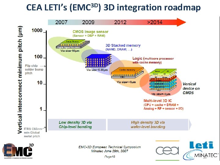
CEA LETI’s (EMC 3 D) 3 D integration roadmap 38

3 D INTEGRATED DEVICE EXAMPLE 39

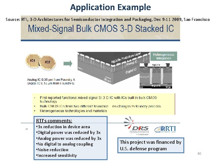
Application Example Source: RTI, 3 -D Architectures for Semiconductor Integration and Packaging, Dec 9 -11 2009, San Francisco RTI’s comments: • 3 x reduction in device area • Digital power was reduced by 3 x • Analog power was reduced by 3 x • No digital to analog coupling • Noise reduction • Increased sensitivity This project was financed by U. S. defense program 40

SUMMARY Via last process might be tried for my chips. However, via middle would have future prospects. HMMM…. 41

Summary • Development of TSV’s has boosted up the development of all the processes used for high-density interconnections. • TSV pilot line processes exist, but commercial processes are only available for few products. • More functionality can be added to packages by heterogeneous integration different technologies - “More than Moore” concept. • 3 D IC’s done at IC foundries, seems to be the most likely way to produce 3 D integrated assemblies. • Economical manufacturing and high-end process aspects. • It will take about two years before commercial processes will be available. • Via middle and via last development are done parallel in HEP community. • Via first, via middle and via last TSV processes are all needed. Each of the is the most suitable from perspective of different applications. • WARNING: Significant technical and economical challenges remain. 42

THANK YOU FOR YOUR ATTENTION 43

BACKUP 44

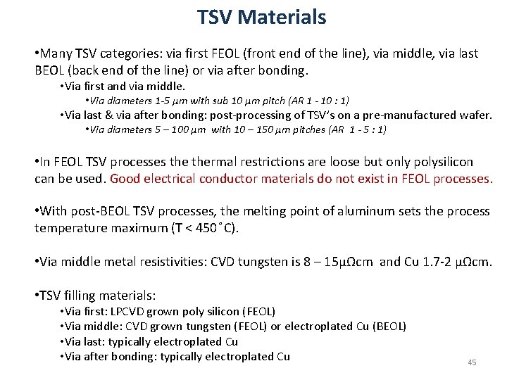
TSV Materials • Many TSV categories: via first FEOL (front end of the line), via middle, via last BEOL (back end of the line) or via after bonding. • Via first and via middle. • Via diameters 1 -5 µm with sub 10 µm pitch (AR 1 - 10 : 1) • Via last & via after bonding: post-processing of TSV’s on a pre-manufactured wafer. • Via diameters 5 – 100 µm with 10 – 150 µm pitches (AR 1 - 5 : 1) • In FEOL TSV processes thermal restrictions are loose but only polysilicon can be used. Good electrical conductor materials do not exist in FEOL processes. • With post-BEOL TSV processes, the melting point of aluminum sets the process temperature maximum (T < 450 C). • Via middle metal resistivities: CVD tungsten is 8 – 15µΩcm and Cu 1. 7 -2 µΩcm. • TSV filling materials: • Via first: LPCVD grown poly silicon (FEOL) • Via middle: CVD grown tungsten (FEOL) or electroplated Cu (BEOL) • Via last: typically electroplated Cu • Via after bonding: typically electroplated Cu 45

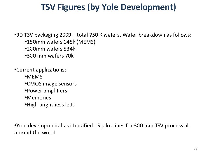
TSV Figures (by Yole Development) • 3 D TSV packaging 2009 – total 750 K wafers. Wafer breakdown as follows: • 150 mm wafers 145 k (MEMS) • 200 mm wafers 534 k • 300 mm wafers 70 k • Current applications: • MEMS • CMOS image sensors • Power amplifiers • Memories • High brightness leds • Yole development has identified 15 pilot lines for 300 mm TSV process all around the world 46