Silicon Crystal Structure and Growth Plummer Chapter 3

- Slides: 60

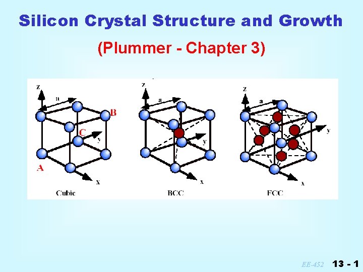
Silicon Crystal Structure and Growth (Plummer - Chapter 3) EE-452 13 - 1

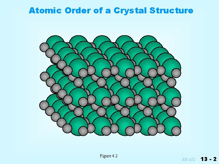
Atomic Order of a Crystal Structure Figure 4. 2 EE-452 13 - 2

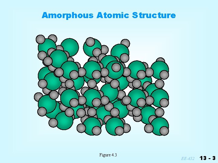
Amorphous Atomic Structure Figure 4. 3 EE-452 13 - 3

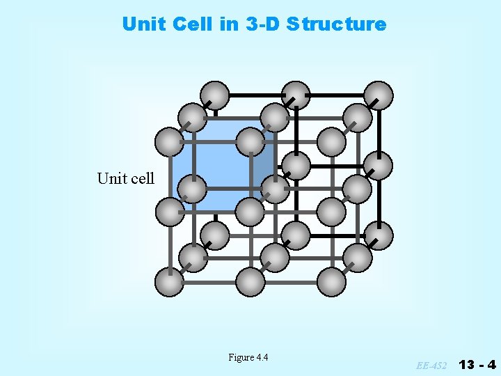
Unit Cell in 3 -D Structure Unit cell Figure 4. 4 EE-452 13 - 4

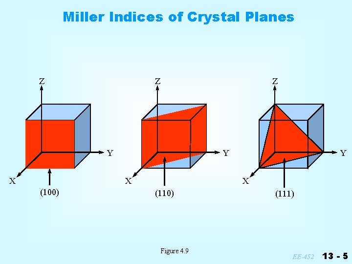
Miller Indices of Crystal Planes Z Z Z Y X (100) Y X (110) Figure 4. 9 (111) EE-452 13 - 5

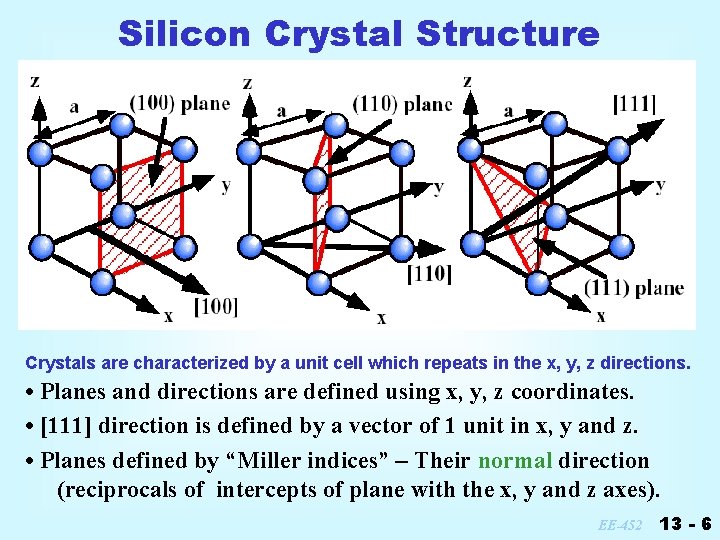
Silicon Crystal Structure Crystals are characterized by a unit cell which repeats in the x, y, z directions. • Planes and directions are defined using x, y, z coordinates. • [111] direction is defined by a vector of 1 unit in x, y and z. • Planes defined by “Miller indices” – Their normal direction (reciprocals of intercepts of plane with the x, y and z axes). EE-452 13 - 6

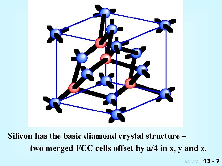
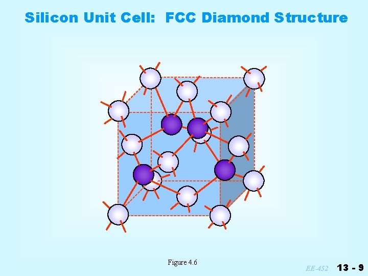
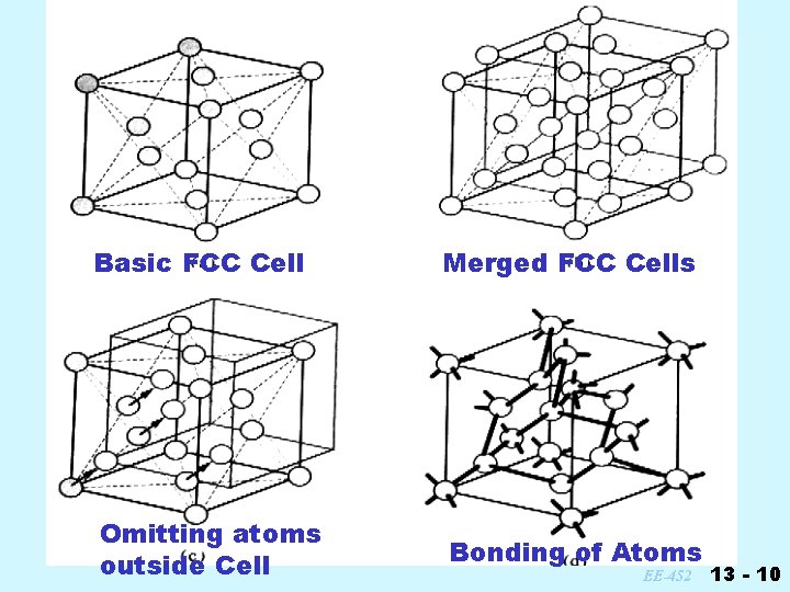
Silicon has the basic diamond crystal structure – two merged FCC cells offset by a/4 in x, y and z. EE-452 13 - 7

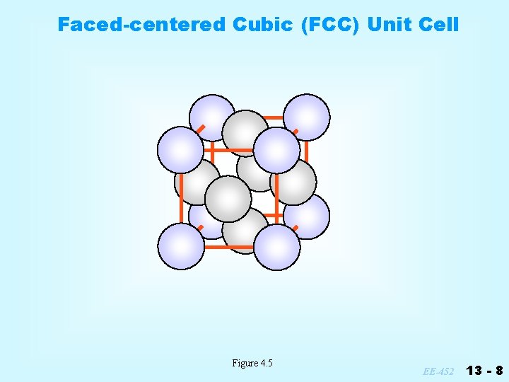
Faced-centered Cubic (FCC) Unit Cell Figure 4. 5 EE-452 13 - 8

Silicon Unit Cell: FCC Diamond Structure Figure 4. 6 EE-452 13 - 9

Basic FCC Cell Merged FCC Cells Omitting atoms outside Cell Bonding of Atoms EE-452 13 - 10

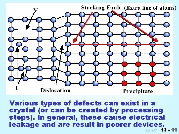
(Extra line of atoms) Various types of defects can exist in a crystal (or can be created by processing steps). In general, these cause electrical leakage and are result in poorer devices. EE-452 13 - 11

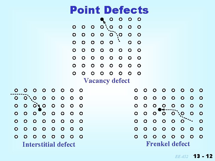
Point Defects Vacancy defect Interstitial defect Frenkel defect EE-452 13 - 12

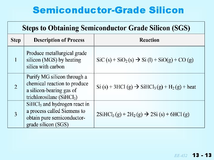
Semiconductor-Grade Silicon EE-452 13 - 13

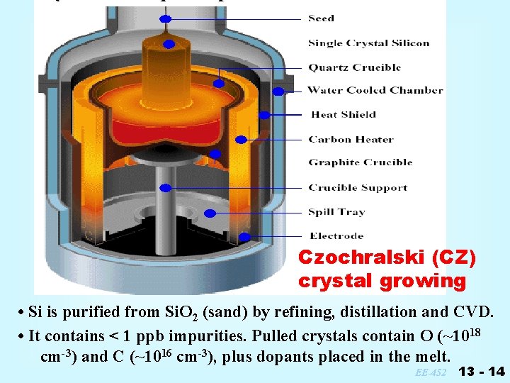
Czochralski (CZ) crystal growing • Si is purified from Si. O 2 (sand) by refining, distillation and CVD. • It contains < 1 ppb impurities. Pulled crystals contain O (~1018 cm-3) and C (~1016 cm-3), plus dopants placed in the melt. EE-452 13 - 14

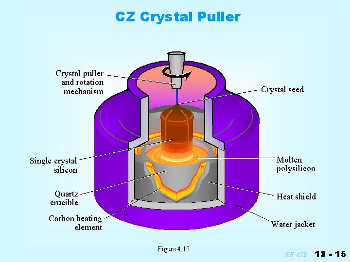
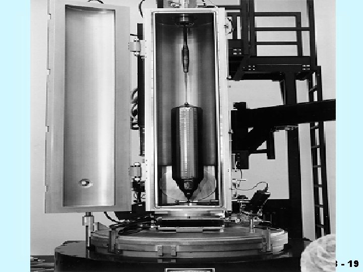
CZ Crystal Puller Crystal puller and rotation mechanism Crystal seed Single crystal silicon Molten polysilicon Quartz crucible Heat shield Carbon heating element Water jacket Figure 4. 10 EE-452 13 - 15

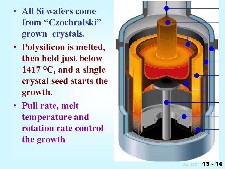
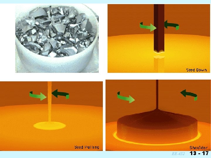
• All Si wafers come from “Czochralski” grown crystals. • Polysilicon is melted, then held just below 1417 °C, and a single crystal seed starts the growth. • Pull rate, melt temperature and rotation rate control the growth EE-452 13 - 16

EE-452 13 - 17

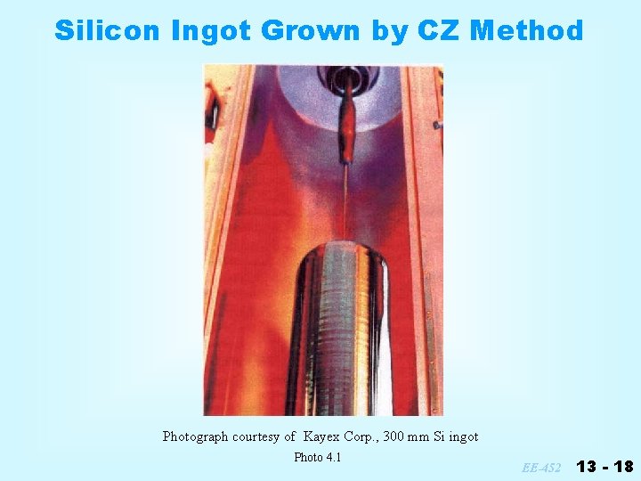
Silicon Ingot Grown by CZ Method Photograph courtesy of Kayex Corp. , 300 mm Si ingot Photo 4. 1 EE-452 13 - 18

EE-452 13 - 19

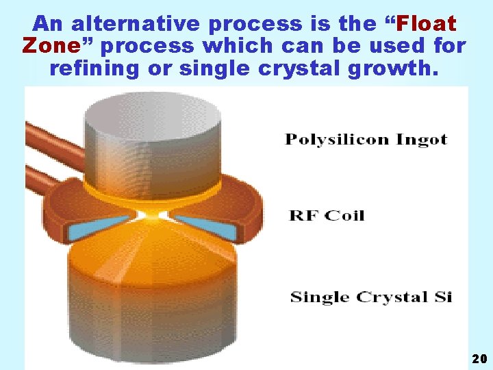
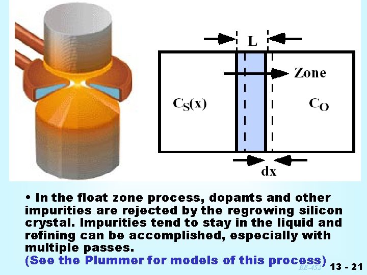
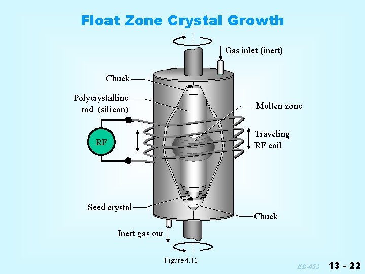
An alternative process is the “Float Zone” process which can be used for refining or single crystal growth. EE-452 13 - 20

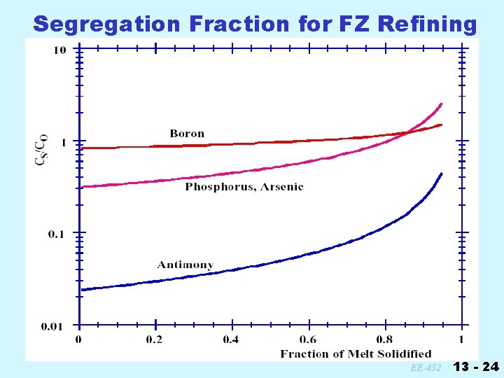
• In the float zone process, dopants and other impurities are rejected by the regrowing silicon crystal. Impurities tend to stay in the liquid and refining can be accomplished, especially with multiple passes. (See the Plummer for models of this process) EE-452 13 - 21

Float Zone Crystal Growth Gas inlet (inert) Chuck Polycrystalline rod (silicon) Molten zone Traveling RF coil RF Seed crystal Chuck Inert gas out Figure 4. 11 EE-452 13 - 22

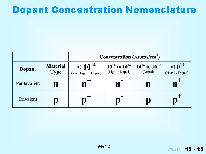
Dopant Concentration Nomenclature Table 4. 2 EE-452 13 - 23

Segregation Fraction for FZ Refining EE-452 13 - 24

Basic Process Steps for Wafer Preparation Crystal Growth Wafer Lapping and Edge Grind Cleaning Shaping Etching Inspection Wafer Slicing Polishing Packaging Figure 4. 19 EE-452 13 - 25

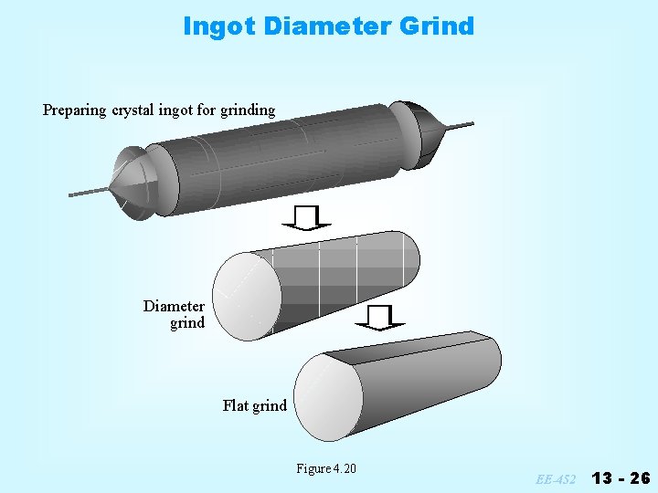
Ingot Diameter Grind Preparing crystal ingot for grinding Diameter grind Flat grind Figure 4. 20 EE-452 13 - 26

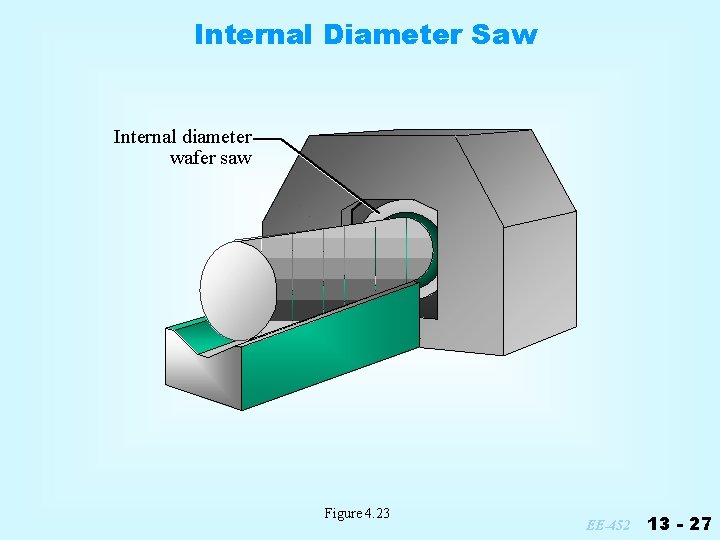
Internal Diameter Saw Internal diameter wafer saw Figure 4. 23 EE-452 13 - 27

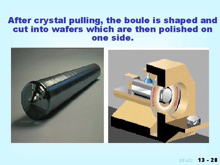
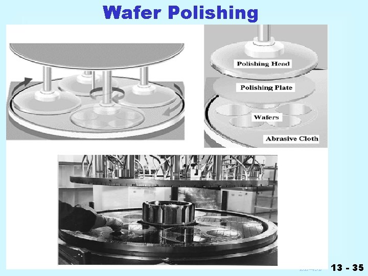
After crystal pulling, the boule is shaped and cut into wafers which are then polished on one side. EE-452 13 - 28

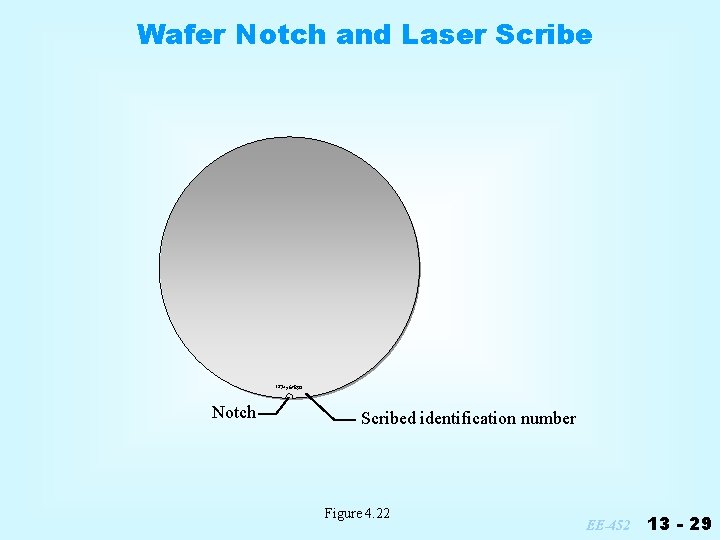
Wafer Notch and Laser Scribe 1234567890 Notch Scribed identification number Figure 4. 22 EE-452 13 - 29

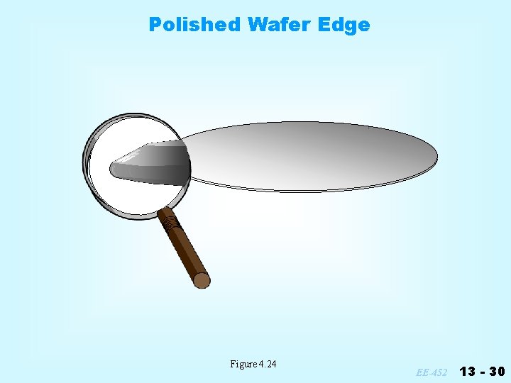
Polished Wafer Edge Figure 4. 24 EE-452 13 - 30

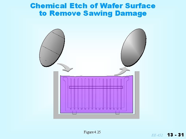
Chemical Etch of Wafer Surface to Remove Sawing Damage Figure 4. 25 EE-452 13 - 31

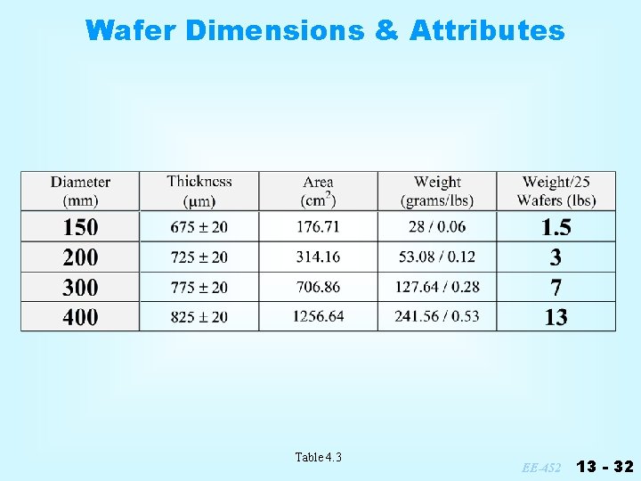
Wafer Dimensions & Attributes Table 4. 3 EE-452 13 - 32

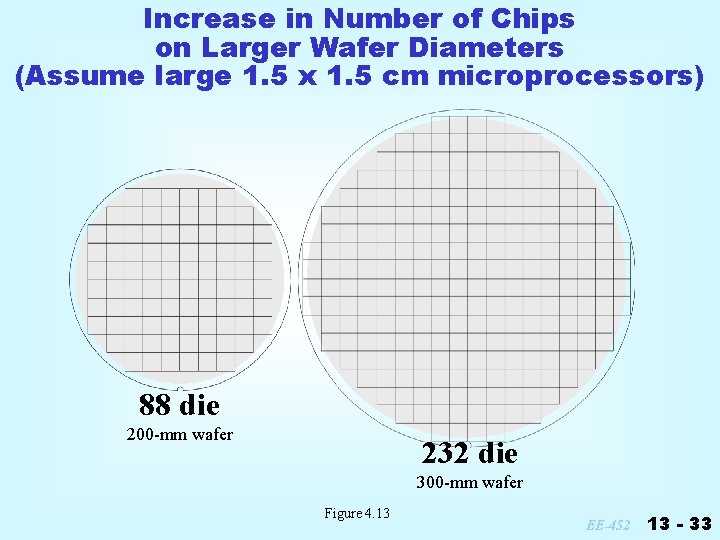
Increase in Number of Chips on Larger Wafer Diameters (Assume large 1. 5 x 1. 5 cm microprocessors) 88 die 200 -mm wafer 232 die 300 -mm wafer Figure 4. 13 EE-452 13 - 33

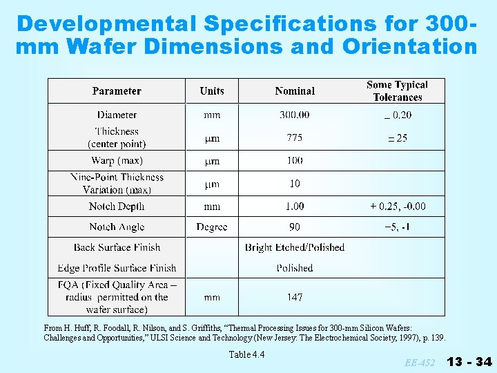
Developmental Specifications for 300 mm Wafer Dimensions and Orientation From H. Huff, R. Foodall, R. Nilson, and S. Griffiths, “Thermal Processing Issues for 300 -mm Silicon Wafers: Challenges and Opportunities, ” ULSI Science and Technology (New Jersey: The Electrochemical Society, 1997), p. 139. Table 4. 4 EE-452 13 - 34

Wafer Polishing EE-452 13 - 35

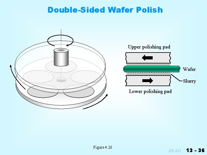
Double-Sided Wafer Polish Upper polishing pad Wafer Slurry Lower polishing pad Figure 4. 26 EE-452 13 - 36

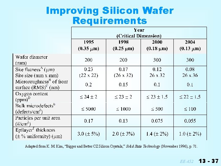
Improving Silicon Wafer Requirements Adapted from K. M. Kim, “Bigger and Better CZ Silicon Crystals, ” Solid State Technology (November 1996), p. 71. EE-452 13 - 37

Quality Measures • • Physical dimensions Flatness Microroughness Oxygen content Crystal defects Particles Bulk resistivity EE-452 13 - 38

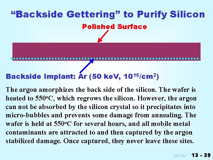
“Backside Gettering” to Purify Silicon Polished Surface Backside Implant: Ar (50 ke. V, 1015/cm 2) The argon amorphizes the back side of the silicon. The wafer is heated to 550 o. C, which regrows the silicon. However, the argon can not be absorbed by the silicon crystal so it precipitates into micro-bubbles and prevents some damage from annealing. The wafer is held at 550 o. C for several hours, and all mobile metal contaminants are attracted to and then captured by the argon stabilized damage. Once captured, they never leave these sites. EE-452 13 - 39

Chapter Review (Wafer Fabrication) • Raw materials (Si. O 2) are refined to produce electronic grade silicon with a purity unmatched by any other available material on earth. • CZ crystal growth produces structurally perfect Si single crystals which are cut into wafers and polished. • Starting wafers contain only dopants, and trace amounts of contaminants O and C in measurable quantities. • Dopants can be incorporated during crystal growth • Point, line, and volume (1 D, 2 D, and 3 D) defects can be present in crystals, particularly after high temperature processing. • Point defects are "fundamental" and their concentration depends on temperature (exponentially), on doping level and on other processes like ion implantation which can create non-equilibrium transient concentrations of these defects. EE-452 13 - 40

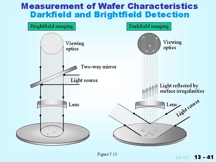
Measurement of Wafer Characteristics Darkfield and Brightfield Detection Darkfield imaging Brightfield imaging Viewing optics Two-way mirror Light source Lens Light reflected by surface irregularities e Lens t igh rc u o s L Figure 7. 15 EE-452 13 - 41

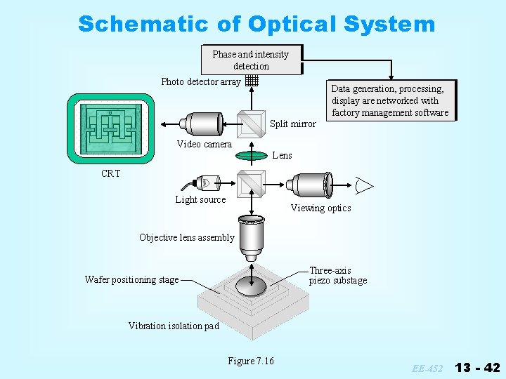
Schematic of Optical System Phase and intensity detection Photo detector array Data generation, processing, display are networked with factory management software Split mirror Video camera Lens CRT Light source Viewing optics Objective lens assembly Three-axis piezo substage Wafer positioning stage Vibration isolation pad Figure 7. 16 EE-452 13 - 42

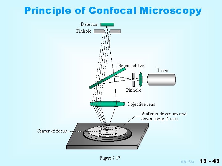
Principle of Confocal Microscopy Detector Pinhole Beam splitter Laser Pinhole Objective lens Wafer is driven up and down along Z-axis Center of focus +Z 0 -Z Figure 7. 17 EE-452 13 - 43

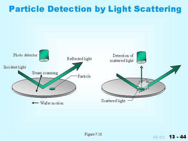
Particle Detection by Light Scattering Photo detector Detection of scattered light Reflected light Incident light Beam scanning Wafer motion Particle Scattered light Figure 7. 18 EE-452 13 - 44

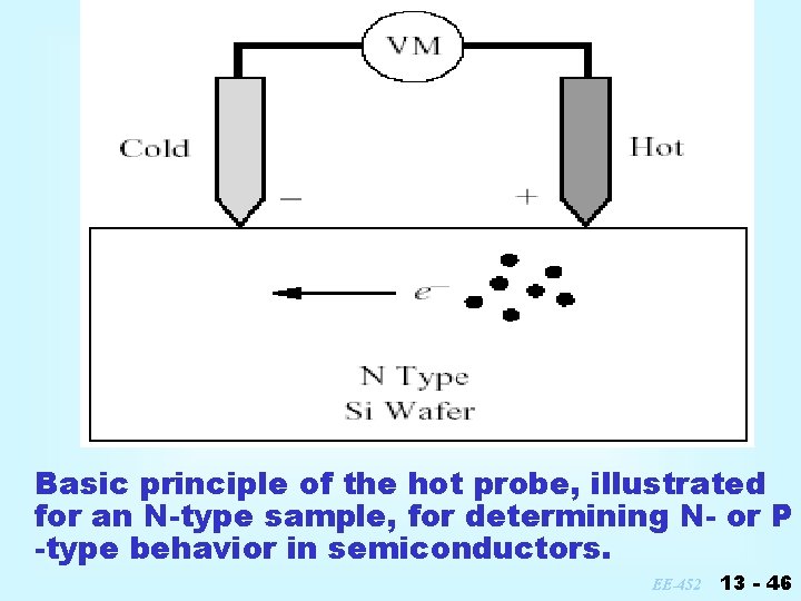
Measurement of Wafer Characteristics Hot Point Probe The hot point probe is a simple and reliable means to determine whether a wafer is N or P type is the Hot Point Probe. The basic operation of this probe is illustrated in the next slide. Two probes make ohmic contact with the wafer surface. One is heated 25 -100°C hotter than the other. A voltmeter placed across the probes will measure a potential difference whose polarity indicates whether the material is N or P type. EE-452 13 - 45

Basic principle of the hot probe, illustrated for an N-type sample, for determining N- or P -type behavior in semiconductors. EE-452 13 - 46

Hot Point Probe Consider an N-type sample. The majority carriers are electrons. At the hot probe, thermal energy of the electrons is higher than at the cold probe so the electrons will tend to diffuse away from the hot probe, driven by the temperature gradient. If a wire were connected between the hot and cold probes, this would result in a measurable current, whose direction would correspond to the electrons moving right to left. (The current by definition would be in the opposite direction. ) If we place a high-impedance voltmeter between the probes, no current flows, but a potential difference is measured, as illustrated. As the electrons diffuse away from the hot probe, they leave behind the positively charged, immobile donor atoms that provided the electrons. The negatively charged mobile electrons tend to build up near the cold probe. This results in the hot probe becoming positive with respect to the cold probe. By a similar set of arguments, if the material were P type, positively charged holes would be the majority carriers and the polarity of the induced voltage would be reversed. The direction of the current between the two probes would also be reversed in P-type material, if they were shorted with a wire. Thus a measurement of either the short-circuit current or the open circuit voltage tells us the type of the material. EE-452 13 - 47

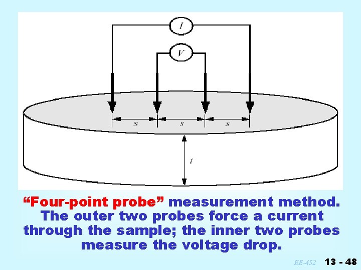
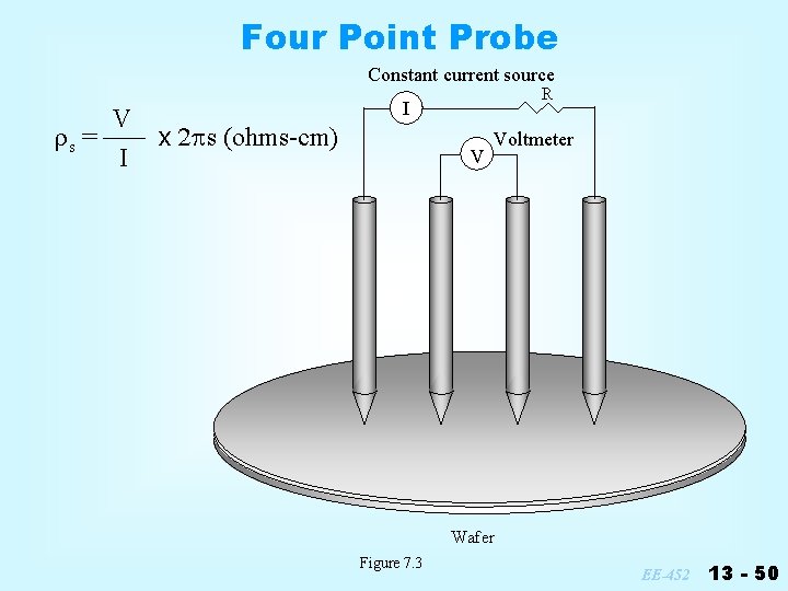
“Four-point probe” measurement method. The outer two probes force a current through the sample; the inner two probes measure the voltage drop. EE-452 13 - 48

Measurement of Sheet Resistance • The most common method of measuring the wafer resistivity is with the four-point probe. We measure the sample resistance by measuring the current that flows for a given applied voltage. This could be done with just two probes. However, in that case, contact resistances associated with the probes and current spreading problems around the probes are important and are not easily accounted for in the analysis. Using four probes allows us to force the current through the two outer probes, where there will still be contact resistance and current spreading problems, but we measure the voltage drop with the two inner probes using a high-impedance voltmeter. Problems with probe contacts are thus eliminated in the voltage measurement since no current flows through these contacts. EE-452 13 - 49

Four Point Probe Constant current source rs = V I x 2 ps (ohms-cm) R I V Voltmeter Wafer Figure 7. 3 EE-452 13 - 50

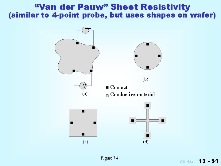
“Van der Pauw” Sheet Resistivity (similar to 4 -point probe, but uses shapes on wafer) I (b) V (a) Contact Conductive material (c) (d) Figure 7. 4 EE-452 13 - 51

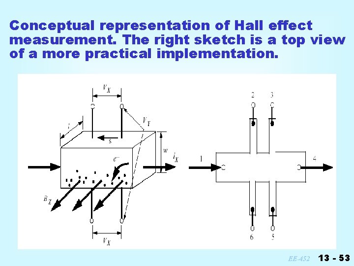
Hall Effect Measurements The Hall effect was discovered more than 100 years ago when Hall observed a transverse voltage across a conductor subjected to a magnetic field. The technique is more powerful than the sheet resistance method described above because it can determine the material type, carrier concentration and carrier mobility separately. The basic method is illustrated in the next slide. The left part of the figure defines the reference directions and the various currents, fields and voltages; the right part of the figure illustrates a top view of a practical geometry that is often used in semiconductor applications. EE-452 13 - 52

Conceptual representation of Hall effect measurement. The right sketch is a top view of a more practical implementation. EE-452 13 - 53

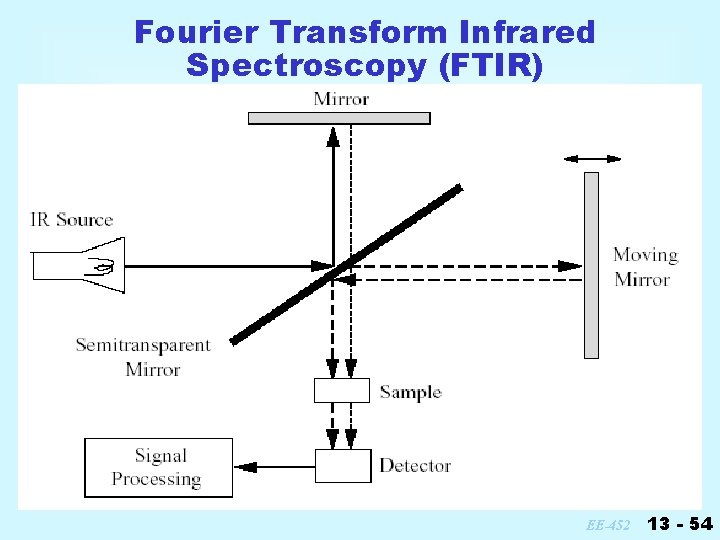
Fourier Transform Infrared Spectroscopy (FTIR) EE-452 13 - 54

FTIR (Oxygen and Carbon Detection) The CZ crystal growth process introduces oxygen and carbon into the silicon. These elements are not inert in the crystal. It is important is to be able to measure them and to control them. The method is Fourier Transform Infrared Spectroscopy. FTIR measures the absorption of infrared energy by the molecules in a sample. Many molecules have vibrational modes that absorb specific wavelengths when they are excited. By sweeping the wavelength of the incident energy and detecting which wavelengths are absorbed, a characteristic signature of the molecules present is obtained. Oxygen in CZ crystals is located in interstitial sites in the silicon lattice, bonded to two silicon atoms. Low concentrations of carbon are substitutional in silicon since carbon is located in the same column of the periodic table as silicon and easily replaces a silicon atom. Oxygen exhibits a vibrational mode that absorbs energy at 1106 cm-1 (wavenumber), that is at a wavelength of about 9 microns; carbon absorbs energy at 607 cm-1. There are other wavelengths of IR light that are absorbed by the silicon atoms themselves. By measuring the absorption of a particular wafer at 1106 or 607 cm -1, and comparing this absorption with an oxygen or carbon free reference, the FTIR technique can be made quantitative. An IR beam is split by a partially reflecting mirror and then follows two separate paths to the sample and the detector. For pure silicon, if the movable mirror is translated back and forth at constant speed, the detected signal will be sinusoidal as the two beams go in and out of phase. The Fourier transform of this signal will simply be a delta function proportional to the incident intensity. If the frequency of the source is swept, the Fourier transform of the resulting signal will produce an intensity spectrum. If we now insert the sample, the resulting intensity spectrum will change because of absorption of specific wavelengths by the sample. The benefit of using the Fourier transform method as opposed to simply directly measuring the intensity spectrum is simply that the signal to noise ratio is improved and as a result, the detection limit is reduced. With modern instruments, the detection limit for interstitial oxygen in silicon is about 2 x 10¹⁵/cm 3. Carbon can be detected down to about 5 x 10¹⁵/cm 3. Oxygen precipitated into small Si. O 2 clusters can be detected by FTIR because in the Si. O 2 form, the oxygen does not absorb at 1106 cm-1. As the precipitation occurs, the IR absorption at this EE-452 13 - 55 wavenumber decreases.

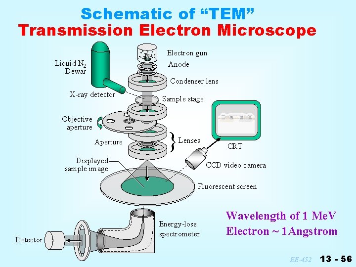
Schematic of “TEM” Transmission Electron Microscope Electron gun Anode Liquid N 2 Dewar Condenser lens X-ray detector Objective aperture Aperture Sample stage } Lenses Displayed sample image CRT CCD video camera Fluorescent screen Detector Energy-loss spectrometer Wavelength of 1 Me. V Electron ~ 1 Angstrom EE-452 13 - 56

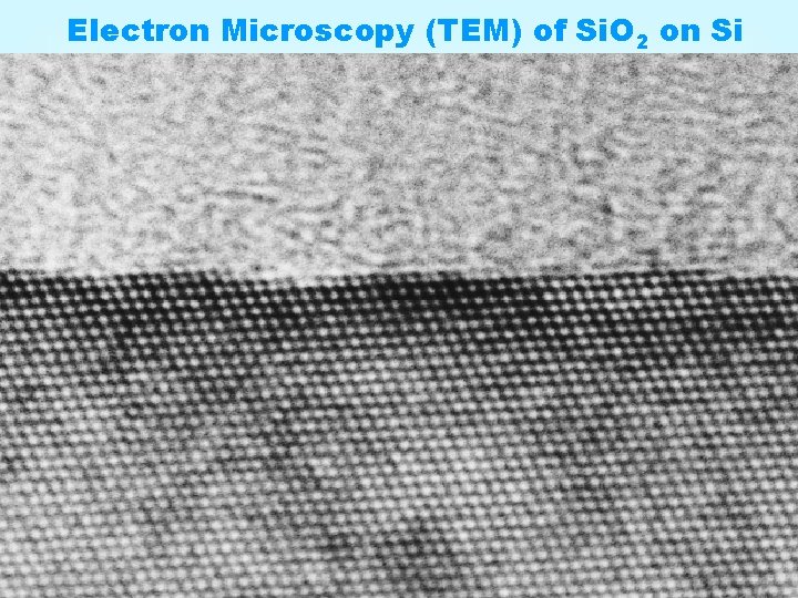
Electron Microscopy (TEM) of Si. O 2 on Si EE-452 13 - 57

Oxygen Contamination in Silicon Oxygen is the most important impurity found in silicon. It is incorporated in silicon during the CZ growth process as a result of dissolution of the quartz crucible in which the molten silicon is contained. The oxygen is typically at a level of about 1018 /cm 3. It has recently become possible to use a magnetic field during CZ growth to control thermal convection currents in the melt. This slows down the transport of oxygen from the crucible walls to the growing silicon interface and reduces the oxygen concentration in the resulting crystal. Oxygen in silicon is always present at concentrations of ~10 -20 ppm (5 x 10¹⁷ - 1018/cm 3) in CZ silicon. The oxygen can affect processes used in wafer fabrication such as impurity diffusion. Oxygen has three principal effects in the silicon crystal. (1) In an as-grown crystal, the oxygen is believed to be incorporated primarily as dispersed single atoms designated OI occupying interstitial positions in the silicon lattice, but covalently bonded to two silicon atoms. The oxygen atoms thus replace one of the normal Si-Si covalent bonds with a Si-O-Si structure. The oxygen atom is neutral in this configuration and can be detected with the FTIR method. Such interstitial oxygen atoms improve the yield strength of silicon by as much as 25%, making silicon wafers more robust in a manufacturing facility. (2) The formation of oxygen donors. A small amount of the oxygen in the crystal forms Si. O 4 complexes which act as donors. They can be detected by changes in the silicon resistivity corresponding to the free electrons donated by the oxygen complexes. As many as 1016/cm 3 donors can be formed, which is sufficient to significantly increase the resistivity of lightly doped P-type wafers. During the CZ growth process, the crystal cools slowly through ~500 o. C temperature and oxygen donors form. The Si. O 4 complexes are unstable at temperatures above 500°C and so usually wafer manufacturers anneal the grown crystal or the wafers themselves after sawing and polishing, to remove the oxygen complexes. These donors can reform, however, during normal IC manufacturing, if a thermal step around 400 -500°C is used. Such steps are not uncommon, particularly at the end of a process flow. (3) The tendency of the oxygen to precipitate under normal device processing conditions, forming Si. O 2 regions inside the wafer. The precipitation arises because the oxygen was incorporated at the melt temperature and is therefore supersaturated in the silicon at process temperatures. EE-452 13 - 58

Carbon Contamination in Silicon Carbon is normally present in CZ grown silicon crystals at concentrations on the order of 1016/cm 3. The carbon comes from the graphite components in the crystal pulling machine. The melt contains silicon and modest concentrations of oxygen. This results in the formation of Si. O that evaporates from the melt surface. Generally, the ambient in the crystal puller is Ar flowing at reduced pressure, and the Si. O can be transported in the gas phase to the graphite crucible and other support fixtures. Si. O reacts with graphite (carbon) to produce CO that again transports through the gas phase back to the melt. From the melt, the carbon is incorporated into the growing crystal. Four Effects of Carbon on Silicon (1) Carbon is mostly substitutional in the silicon lattice. Since it is a column IV element, it does not act as a donor or acceptor in silicon. Carbon is known to affect the precipitation kinetics of oxygen in silicon. This is likely because there is a volume expansion when oxygen precipitates and a volume contraction when carbon precipitates because of the relative sizes of O and C. There is thus a tendency for precipitates that are complexes of C and O to form at minimum stresses in the crystal. Since precipitated Si. O 2 is crucial in intrinsic gettering, this can have an effect on gettering efficiency. (2) Carbon is also known to interact with point defects in silicon. Silicon interstitials tend to displace carbon atoms from lattice sites, presumably because this can help to compensate the volume contraction present when there is carbon in the crystal. (3) Thermal donors (Oxygen Effects) normally form around 450°C. There is also evidence that if C is present at ~1 ppm, these donors may also form at higher temperatures (650 -1000°C). (4) Higher concentrations of C to Si (levels of a few percent) can change the bandgap of the silicon and may allow the fabrication of new types of semiconductor devices in the future. EE-452 13 - 59

Chapter Review (Wafer Metrology) • • Microscopic examination for particulates. Hot Point Probe (wafer doping) Four Point Probe (wafer resistivity) Hall Effect (carrier mobility) FBIR (oxygen and carbon detection) TEM (atomic resolution of defects / surface) Effects of Oxygen on IC fabrication Effects of Carbon on IC fabrication EE-452 13 - 60