450 mm Wafers Size Conversion 20201030 ITRS Factory
![Important Roadmap Points for 450 mm ¬ Wafer size conversion will be economically [productivity] Important Roadmap Points for 450 mm ¬ Wafer size conversion will be economically [productivity]](https://slidetodoc.com/presentation_image/2bc2d5d435f6c1f9fea4bae94ce61df9/image-3.jpg)
- Slides: 4

450 mm Wafers Size Conversion 2020/10/30 ITRS Factory Integration TWG 1

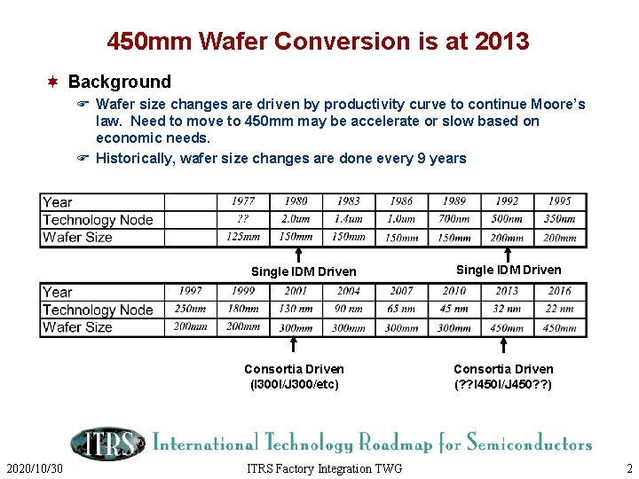
450 mm Wafer Conversion is at 2013 ¬ Background F Wafer size changes are driven by productivity curve to continue Moore’s law. Need to move to 450 mm may be accelerate or slow based on economic needs. F Historically, wafer size changes are done every 9 years Single IDM Driven Consortia Driven (I 300 I/J 300/etc) 2020/10/30 ITRS Factory Integration TWG Single IDM Driven Consortia Driven (? ? I 450 I/J 450? ? ) 2
![Important Roadmap Points for 450 mm Wafer size conversion will be economically productivity Important Roadmap Points for 450 mm ¬ Wafer size conversion will be economically [productivity]](https://slidetodoc.com/presentation_image/2bc2d5d435f6c1f9fea4bae94ce61df9/image-3.jpg)
Important Roadmap Points for 450 mm ¬ Wafer size conversion will be economically [productivity] driven ¬ Based on 300 mm key learning, 5 -6 years are required to develop methods (eg 25 wafer FOUP), standards, equipment, and to start pilot production prior to high volume manufacturing F Consortia’s (ex. J 300/I 300 I/ISMT/SELETE) will drive timing, methods, and standards ¬ Basic research should start 2 -3 years before this applied development ¬ For a 2013 intercept, this means that development should start 2007 and research should start 2005 (2 major roadmap changes from now) ¬ Industry will likely undergo major change from bulk CMOS technology to other device structures in 2010. F As a result, a wafer size change may not occur at the same timeframe 2001 2002 2003 2004 2005 2006 2007 2008 2009 2010 2011 2012 2013 2014 2015 Basic 450 mm Research Development of Methods, Standards, equipment, solutions Pilot Line -> HVM Factory 2001 2020/10/30 2002 2003 2004 2005 2006 2007 2008 2009 2010 2011 ITRS Factory Integration TWG 2012 2013 3

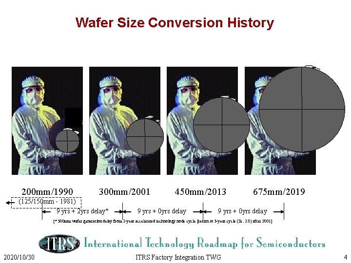
Wafer Size Conversion History 200 mm/1990 300 mm/2001 (125/150 mm - 1981) 9 yrs + 2 yrs delay* 450 mm/2013 9 yrs + 0 yrs delay 675 mm/2019 9 yrs + 0 yrs delay [* 300 mm wafer generation delay from 2 -year accelerated technology node cycle [return to 3 -year cycle (Sc. 2. 0) after 2001] 2020/10/30 ITRS Factory Integration TWG 4