Room Temperature Mechanical Loss of Silicon Nitride Silica
- Slides: 12
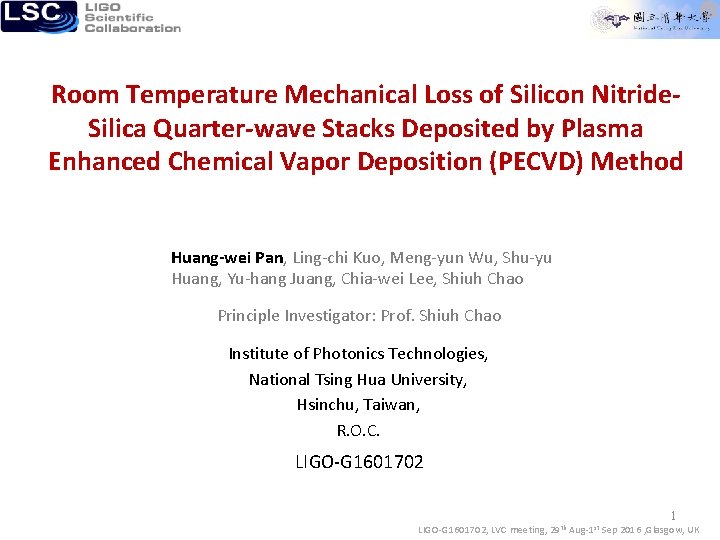
Room Temperature Mechanical Loss of Silicon Nitride. Silica Quarter-wave Stacks Deposited by Plasma Enhanced Chemical Vapor Deposition (PECVD) Method Huang-wei Pan, Ling-chi Kuo, Meng-yun Wu, Shu-yu Huang, Yu-hang Juang, Chia-wei Lee, Shiuh Chao Principle Investigator: Prof. Shiuh Chao Institute of Photonics Technologies, National Tsing Hua University, Hsinchu, Taiwan, R. O. C. LIGO-G 1601702 1 LIGO-G 1601702, LVC meeting, 29 th Aug-1 st Sep 2016 , Glasgow, UK
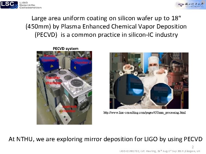
Large area uniform coating on silicon wafer up to 18“ (450 mm) by Plasma Enhanced Chemical Vapor Deposition (PECVD) is a common practice in silicon-IC industry http: //www. linx-consulting. com/pages/450 mm_processing. html At NTHU, we are exploring mirror deposition for LIGO by using PECVD 2 LIGO-G 1601702, LVC meeting, 29 th Aug-1 st Sep 2016 , Glasgow, UK
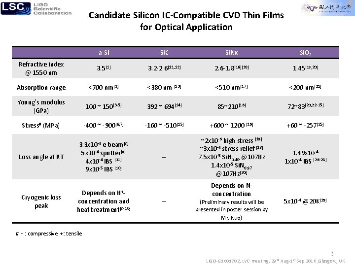
Candidate Silicon IC-Compatible CVD Thin Films for Optical Application a-Si Si. C Si. Nx Si. O 2 Refractive index @ 1550 nm 3. 5[1] 3. 2 -2. 6[11, 12] 2. 6 -1. 8[16][30] 1. 45[19, 20] Absorption range <700 nm[2] <380 nm [13] <510 nm[17] <200 nm[21] Young’s modulus (GPa) 100 ~ 150[3 -5] 392 ~ 694[14] 85~210[16] 72~83[20, 22 -25] Stress# (MPa) -400 ~ -900[6, 7] -160 ~ -510[15] +600 ~ 1200 [16] +60 ~ -257[25] Loss angle at RT 3. 3 x 10 -4 e beam[8] 5 x 10 -4 sputter[8] 4 x 10 -4 IBS [31] 9 x 10 -5 IBS [10] -- ~2 x 10 -6 high stress [18] ~3 x 10 -4 stress relief [18] 7. 5 x 10 -5 Si. N 0. 40 @107 Hz 1. 4 x 10 -5 Si. N 0. 87 @107 Hz[30] 1. 49 x 10 -4 1 x 10 -4 IBS [26 -28] Cryogenic loss peak H +- Depends on concentration and heat treatment[8 -10] -- Depends on Nconcentration 5 x 10 -4 @20 K[29] (Preliminary results will be presented in poster session by Mr. Kuo) # - : compressive +: tensile 3 LIGO-G 1601702, LVC meeting, 29 th Aug-1 st Sep 2016 , Glasgow, UK
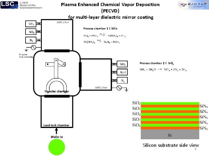
Plasma Enhanced Chemical Vapor Deposition (PECVD) for multi-layer dielectric mirror coating Process chamber 1:Si. Nx Process chamber 2: Si. O 2 Silicon substrate side view 4 LIGO-G 1601702, LVC meeting, 29 th Aug-1 st Sep 2016 , Glasgow, UK
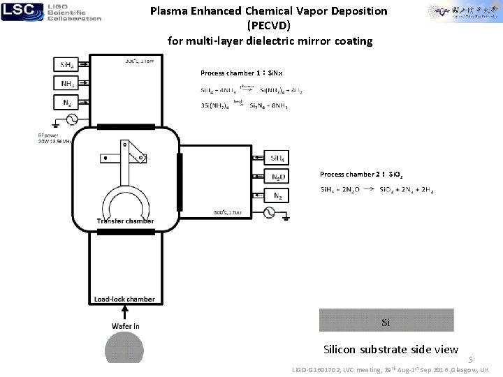
Plasma Enhanced Chemical Vapor Deposition (PECVD) for multi-layer dielectric mirror coating Process chamber 1:Si. Nx Process chamber 2: Si. O 2 Silicon substrate side view LIGO-G 1601702, LVC meeting, 29 th Aug-1 st 5 Sep 2016 , Glasgow, UK
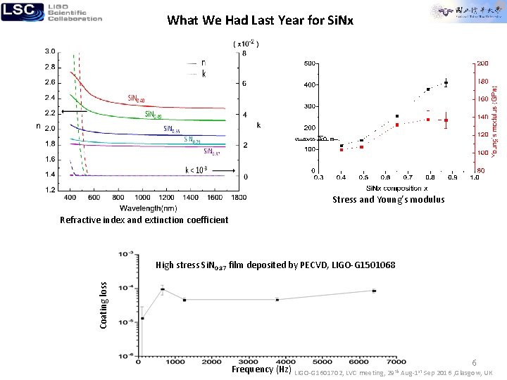
What We Had Last Year for Si. Nx Stress and Young’s modulus Refractive index and extinction coefficient Coating loss High stress Si. N 0. 87 film deposited by PECVD, LIGO-G 1501068 6 Frequency (Hz) LIGO-G 1601702, LVC meeting, 29 th Aug-1 st Sep 2016 , Glasgow, UK
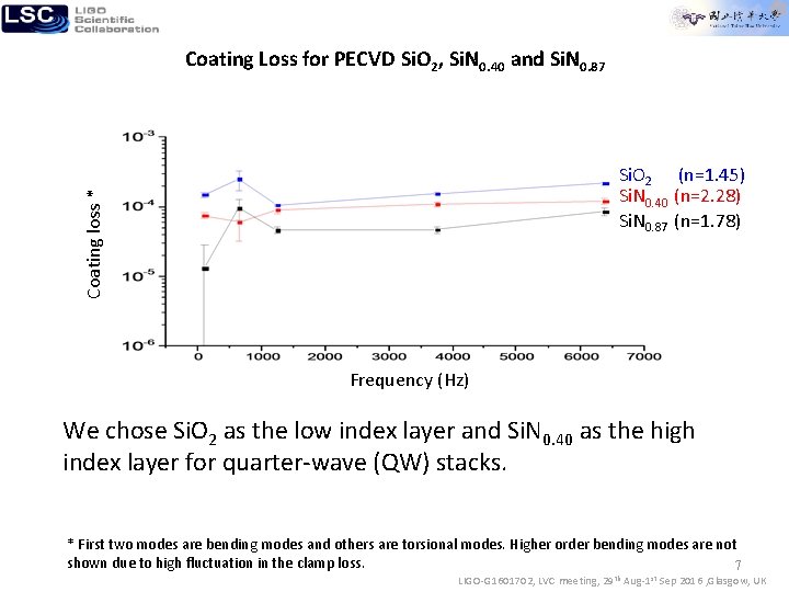
Coating Loss for PECVD Si. O 2, Si. N 0. 40 and Si. N 0. 87 Coating loss * Si. O 2 (n=1. 45) Si. N 0. 40 (n=2. 28) Si. N 0. 87 (n=1. 78) Frequency (Hz) We chose Si. O 2 as the low index layer and Si. N 0. 40 as the high index layer for quarter-wave (QW) stacks. * First two modes are bending modes and others are torsional modes. Higher order bending modes are not shown due to high fluctuation in the clamp loss. 7 LIGO-G 1601702, LVC meeting, 29 th Aug-1 st Sep 2016 , Glasgow, UK
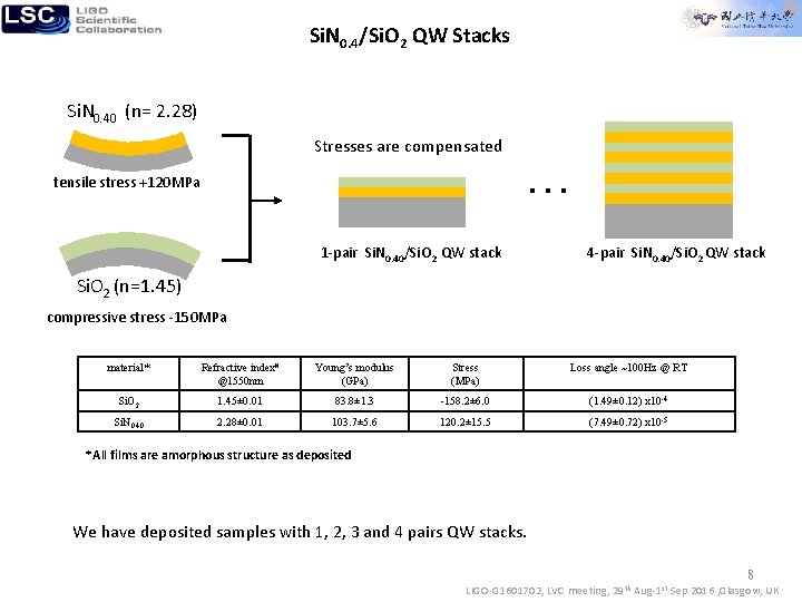
Si. N 0. 4/Si. O 2 QW Stacks Si. N 0. 40 (n= 2. 28) Stresses are compensated tensile stress +120 MPa ‧‧‧ 1 -pair Si. N 0. 40/Si. O 2 QW stack 4 -pair Si. N 0. 40/Si. O 2 QW stack Si. O 2 (n=1. 45) compressive stress -150 MPa material* Refractive index# @1550 nm Young’s modulus (GPa) Stress (MPa) Loss angle ~100 Hz @ RT Si. O 2 1. 45± 0. 01 83. 8± 1. 3 -158. 2± 6. 0 (1. 49± 0. 12) x 10 -4 Si. N 0. 40 2. 28± 0. 01 103. 7± 5. 6 120. 2± 15. 5 (7. 49± 0. 72) x 10 -5 *All films are amorphous structure as deposited We have deposited samples with 1, 2, 3 and 4 pairs QW stacks. 8 LIGO-G 1601702, LVC meeting, 29 th Aug-1 st Sep 2016 , Glasgow, UK
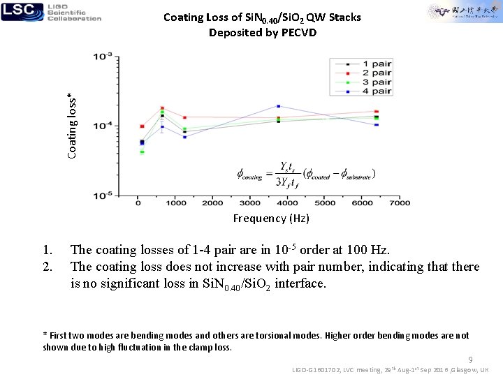
Coating loss* Coating Loss of Si. N 0. 40/Si. O 2 QW Stacks Deposited by PECVD Frequency (Hz) 1. 2. The coating losses of 1 -4 pair are in 10 -5 order at 100 Hz. The coating loss does not increase with pair number, indicating that there is no significant loss in Si. N 0. 40/Si. O 2 interface. * First two modes are bending modes and others are torsional modes. Higher order bending modes are not shown due to high fluctuation in the clamp loss. 9 LIGO-G 1601702, LVC meeting, 29 th Aug-1 st Sep 2016 , Glasgow, UK
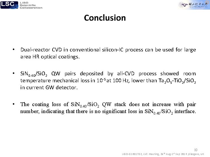
Conclusion • Dual-reactor CVD in conventional silicon-IC process can be used for large area HR optical coatings. • Si. N 0. 40/Si. O 2 QW pairs deposited by all-CVD process showed room temperature mechanical loss in 10 -5 at 100 Hz, lower than Ta 2 O 5 -Ti. O 2/Si. O 2 in current GW detector. • The coating loss of Si. N 0. 40/Si. O 2 QW stack does not increase with pair number, indicating that there is no significant loss in Si. N 0. 40/Si. O 2 interface. 10 LIGO-G 1601702, LVC meeting, 29 th Aug-1 st Sep 2016 , Glasgow, UK
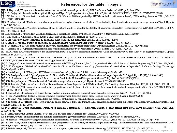
References for the table in page 3 [1]B. J. Frey, et al, “Temperature-dependent refractive index of silicon and germanium”, SPIE Conference Series, vol. 6273, p. 2, June 2006. [2] G. D. Cody, et al, “Disorder and the optical-Absorption Edge of Hydrogenated Amorphous Silicon” , Vol. 47 No. 20 PHYS REV. LETT. 16 NOVEMBER (1981) [3] H. W. Pan, et al, “Stress effect on mechanical loss of Si. NX and α-Si film deposited by PECVD method on silicon cantilever”, LVC meeting, Pasadena USA, , Mar. 17 th , 2015, LIGO- G 1500195, [4] R. Kuschnereit, et al, “Mechanical and elastic properties of amorphous hydrogenated silicon films studied by broadband surface acoustic wave spectroscopy” Appl. Phys. A 61, 269 -276 (1995) [5] R. B. Wehrspohn et al, “Relative importance of the Si–Si bond and Si–H bond for the stability of amorphous silicon thin film transistors”, J. APPLIED PHYSICS VOL 87, No 11, JANUARY (2000) [6] C. K. Chung, et al “Fabrication and characterization of amorphous Si films by PECVD for MEMS”, J. Micromech. Microeng. 15 (2005). [7] P Danesh, et al, “Mechanical stress in thin a-Si: H films”, Semicond. Sci. Technol. 15 (2000) 971– 974. [8] X. Liu et al, “low energy excitations in amorphous films of silicon and germanium”, Phys. Rev. B 58, 9067 (1998). [9] X. Liu, et al, “Internal friction of amorphous and nanocrystalline silicon at low temperatures”, Mater. Sci. Eng. 442, 307 (2006). [10]P. G. Murray, et al, “Ion-beam sputtered amorphous silicon films for cryogenic precision measurement systems”, Phys. Rev. D 92, 062001 (2015) [11] J Cardenas, et al, “Optical nonlinearities in high-confinement silicon carbide waveguides”, Optics Letters Vol. 40, No. 17, 2015. [12] M. A. Nigro et al. “Measurement of the IR absorption induced by visible radiation in amorphous silicon and silicon carbide thin films by an in-guide technique”, Optical Materials 30 (2008) 1240– 1243 [13] J. B. CASADY, “STATUS OF SILICON CARBIDE (SIC) AS A Wl. DE-BANDGAP SEMICONDUCTOR FOR HIGH-TEMPERATURE APPLICATIONS: A REVIEW”, Solid-State Electronics Vol. 39, No. I 0, pp. 1409 -1422, 1996 [14] L. Jiang, et al “A review of silicon carbide development in MEMS applications”, Int. J. Computational Materials Science and Surface Engineering, Vol. 2, Nos. 3/4, 2009. [15] C. K. Chung et al, “Global and local residual stress in silicon carbide films produced by plasma-enhanced chemical vapor deposition”, Surface & Coatings Technology 200 (2006) 4825 – 4834 [16] A Stoffel, et al, “LPCVD against PECVD for micromechanical applications”, J. Micromech. Microeng. 6 (1996) 1– 13. [17] S. V. Deshpande, et al, “ Optical properties of silicon nltride films deposited by hot filament chemical vapor deposition”, J, Appl. Phys. 77 (12), 15 June (1995) [18] D. R. Southworth , et al. “Stress and Silicon Nitride A Crack in the Universal Dissipation of Glasses”, Phys. Rev. Lett. 102. 225503(2009) [19] V. B. Braginsky, et al, “Thermodynamical fluctuations in optical mirror coatings”, Physics Letters A 312 (2003) 244– 255 [20]H. W. Pan, et al, “Mechanical loss of silica film on silicon cantilever deposited by PECVD method”, LVC meeting, Pasadena, USA, Mar. 17 th , 2015, LIGO-G 1500194 [21] Y. N. Xu, et al, “Electronic structure and optical properties of a and P phases of silicon nitride, silicon oxynitride, and with comparison to silicon dioxide”, PHYS. REV. B VOL 51, No. 24 15 JUNE (1995). [22] J. Thum, et al, “Stress hysteresis during thermal cycling of plasma-enhanced chemical vapor deposited silicon oxide films”, J. Appli. Phys. 91, 2002, [23] Z. Cao , “Microbridge testing of plasma-enhanced chemical-vapor deposited silicon oxide films on silicon wafers”, J. Appli. Phys. 97, 2005 [24] Y. G. Jung , “Evaluation of elastic modulus and hardness of thin films by nanoindentation”, J. Mater. Res. 19, 2004, [25] J. K. Choia , et al, “Effects of process parameters on the growth of thick Si. O 2 using plasma enhanced chemical vapor deposition with hexamethyldisilazane”, Surface and Coatings Technology 131 2000. [26]D. R. Crooks, et al, “Experimental measurements of mechanical dissipation associated with dielectric coatings formed using Si. O 2, Ta 2 O 5 and Al 2 O 3”Class. Quan. Grav. 23 (2006)4953 -4965 [27]S. Penn, “Exploring Coating Thermal Noise via Loss in Fused Silica Coatings”Proc. Amaldi 2009, LIGO -G 0900600 [28]I. Martin, “Studies of materials for use in future interferometric gravitational wave detectors”, Ph. D thesis, University of Glasgow, (2009) [29] M. Principe, “Reflective coating optimization for interferometric detectors of gravitational waves”, Vol. 23, No. 9 OPTICS EXPRESS, 4 May 2015 p. 10938 [30] S. Chao, et al, “Room temperature mechanical loss of high stress silicon nitride film measured by cantilever ring‐down method on double‐side coated cantilever” LVC meeting, Budapest, Hungary, Sep. 1 st , 2015, LIGO‐G 1501068 11 [31] J. Steinlechner, et al, “Thermal noise reduction and absorption optimization via multimaterial coatings”, PHYSICAL REVIEW D 91, 042001 (2015) LIGO-G 1601702, LVC meeting, 29 th Aug-1 st Sep 2016 , Glasgow, UK
Thank You For Your Attention 12 LIGO-G 1601702, LVC meeting, 29 th Aug-1 st Sep 2016 , Glasgow, UK