Computer Organization and Architecture Themes and Variations 1

- Slides: 126

Computer Organization and Architecture: Themes and Variations, 1 st Edition CHAPTER 10 Computer Organization and Architecture 1 © 2014 Cengage Learning Engineering. All Rights Reserved. Clements

Computer Organization and Architecture: Themes and Variations, 1 st Edition Clements Main Memory 2 © 2014 Cengage Learning Engineering. All Rights Reserved.

In this chapter we look at the operating principles of immediate access memory, the difference between static and dynamic classes of memory, and the difference between volatile and non-volatile memory. We also introduce some of the new technologies that are beginning to play a significant role in memory systems. As well as the characteristics of memory devices we also look at some of the considerations that the memory systems designer has to take into account. 3 © 2014 Cengage Learning Engineering. All Rights Reserved.

Dynamic – the misnomer The main store of most computers uses dynamic memory, DRAM. The term dynamic is rather misleading. The normal English usage of dynamic implies a positive, even aggressive, level of performance. However, its use in DRAM means the reverse. Data is stored as an electric charge that leaks away over a few milliseconds. In other words, DRAM loses its data in a few milliseconds. Data can be retained in the DRAM only by continually reading it before it disappears and writing it back. The term dynamic indicates this property. (Perhaps the ‘D’ in DRAM should stand for drippy). 4 © 2014 Cengage Learning Engineering. All Rights Reserved.

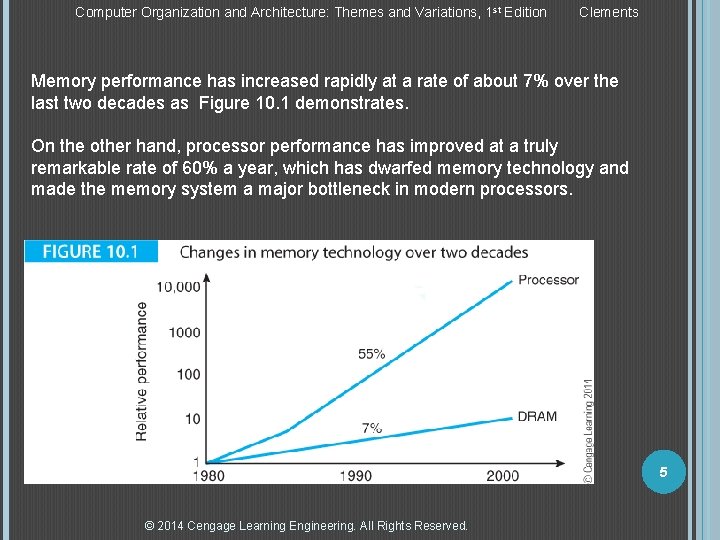
Computer Organization and Architecture: Themes and Variations, 1 st Edition Clements Memory performance has increased rapidly at a rate of about 7% over the last two decades as Figure 10. 1 demonstrates. On the other hand, processor performance has improved at a truly remarkable rate of 60% a year, which has dwarfed memory technology and made the memory system a major bottleneck in modern processors. 5 © 2014 Cengage Learning Engineering. All Rights Reserved.

Computer Organization and Architecture: Themes and Variations, 1 st Edition Clements Principles and Parameters of Memory Systems The range of physical properties that have been exploited to store data is quite remarkable. In the late 1940 s columns of mercury in tubes were used to store data as sound in motion. At one end of the tube data in the form of a sequence of ultrasonic pulses was transmitted down the tube traveling at the speed of sound in mercury (1, 450 m/s). When the sound reached the far end of the tube, it was picked up by transducers, amplified and fed back to the other end of the tube. 6 © 2014 Cengage Learning Engineering. All Rights Reserved.

Computer Organization and Architecture: Themes and Variations, 1 st Edition Clements Between the 1950 s and 1970 s data was stored as a magnetic field in a tiny bead (or toroid) of a magnetic material called a ferrite core (hence the term core memory that often crops up in computer literature). Today’s hard disk drives still use the same magnetic phenomenon to store data. Because of its importance, we look at magnetic recording in detail in the next chapter. From the mid-1970 s on, semiconductor memory provided the standard form of main store memory; either as semiconductor static RAM (SRAM) or as dynamic RAM (DRAM). Today only small embedded systems use static RAM and PCs employ about 2 to 48 GB of DRAM. 7 © 2014 Cengage Learning Engineering. All Rights Reserved.

Computer Organization and Architecture: Themes and Variations, 1 st Edition Clements If DRAM is theme of this chapter, the variations are provided by some of the newer form of semiconductor memory: • semiconductor ferroelectric memory that stores data as the position of an atom within a crystal • ovonic memory that stores data by switching a glass-like material called a chalcogenide between an amorphous state and a polycrystalline state. 8 © 2014 Cengage Learning Engineering. All Rights Reserved.

Computer Organization and Architecture: Themes and Variations, 1 st Edition Clements Random Access and Sequential Access Memory A fundamental distinction between the various memory technologies used in computers is the way in which data is accessed; directly or sequentially. Memory that is directly accessed is called random access memory, RAM, because you can access any data element at random and the time taken to perform the access is constant and effectively independent of the physical location of the data. Such memories are also called immediate access memories, IAS. Of course, these memories aren’t really immediate access – nothing is immediate; they are just so much faster than other types of memory. 9 © 2014 Cengage Learning Engineering. All Rights Reserved.

Computer Organization and Architecture: Themes and Variations, 1 st Edition Clements Sequential access memory requires you to access each memory element in turn until you locate the element you are seeking. An example of a sequential access memory is the magnetic tape store; you have to read the tape until you find the item you want. The acoustic mercury delay line memory that we mentioned earlier is also a sequential access memory. Random access memories are invariably faster than sequential access memories, but they are also much more expensive. Most semiconductor memory such as DRAM or flash memory is random access. The shift register is, or course, a serial access memory. We often speak of the speed of memory or say how fast or slow it is. These terms refer to how long it takes to access data. The key parameter of memory is tacc, its access time. 10 © 2014 Cengage Learning Engineering. All Rights Reserved.

Computer Organization and Architecture: Themes and Variations, 1 st Edition Clements Random and Serial Access You should be aware that serial access is sometimes used differently by hardware and software people. A memory is serial access if the device reading it has to step through several elements to find the desired data. In the software world, a file on a disk is considered random access if you can access an element without reading other elements in a data structure. However, the underlying storage device, the disk, is serial access because it is rotating and you have to wait for the required data to pass under the read head. 11 © 2014 Cengage Learning Engineering. All Rights Reserved.

Computer Organization and Architecture: Themes and Variations, 1 st Edition Clements Volatile and Non-volatile Memory If you store data in an ideal memory, it stays there until you explicitly modify it. Such a memory is called non-volatile; for example, when you write data to a hard disk, the data remains on the hard disk indefinitely. Some memory technologies retain stored data only as long as they receive electric power – pull the plug and the data is gone These memories are said to be volatile because data evaporates in the absence of power. The main stores of most PCs and workstations are composed of DRAM volatile memory. If the memory were non-volatile, you wouldn’t have to boot the computer (i. e. , transfer the operating system from non-volatile memory on disk to volatile memory within the computer) each time you switch the power on. 12 © 2014 Cengage Learning Engineering. All Rights Reserved.

Computer Organization and Architecture: Themes and Variations, 1 st Edition Clements Read/write and Read-only Memory A computer’s main store is, of course, composed of read/write memory. If the memory can easily be read but its contents can’t be modified, it is said to be read-only memory. Read-only memory is invariably non-volatile. Practical read-only memory is better described as read-mostly memory that can be modified a limited number of times. Moreover, it requires a more complex and slower write operation than a read operation. Examples of read-mostly memory are EPROM, EEPROM, and flash memory. 13 © 2014 Cengage Learning Engineering. All Rights Reserved.

Computer Organization and Architecture: Themes and Variations, 1 st Edition Clements Static and Dynamic Memory Random access, read-write, volatile memory can be divided into two subclasses; static and dynamic. These classes refer to the structure of semiconductor memory cells and their properties. Static memory uses cross-coupled transistors to create an RS flip-flop that stores the data in the state of the flip-flop. Dynamic memory, DRAM, employs a semiconductor technology that stores data as an electrostatic charge in a capacitor. Static memory is faster, more expensive, and less dense (bits per chip) than its dynamic counterpart. Dynamic memory is much cheaper than static memory but is more difficult to use in actual circuits. This statement is less true today. Today, DRAM control is built into CPUs, motherboard bridge chips, and the DRAMs themselves. In the 1980 s building a DRAM controller into your computer was a daunting task. 14 © 2014 Cengage Learning Engineering. All Rights Reserved.

Computer Organization and Architecture: Themes and Variations, 1 st Edition Clements The data in a dynamic memory cell is lost after a few milliseconds unless it is continually rewritten in an operation called refreshing. Dynamic memory has different read and write access times and typical DRAM is not truly random access because adjacent memory cells are faster to access than cells selected at random. Because DRAM forms the bulk of most PC and workstation memories, the performance and characteristics of DRAM strongly determine the overall performance of computers. 15 © 2014 Cengage Learning Engineering. All Rights Reserved.

Computer Organization and Architecture: Themes and Variations, 1 st Edition Clements Memory Parameters The smallest unit of memory is the memory cell that stores a single bit. Semiconductor memories are organized as an array of n rows by m columns; that is they contain n x m cells. The width of the memory, m, is the number of bits per word in the memory. When a read or write operation is executed, all m bits of a word take place in the operation simultaneously. The length of the memory, n, is defined as the number of addressable locations (i. e. , the memory employs n address lines to select 2 n locations). 16 © 2014 Cengage Learning Engineering. All Rights Reserved.

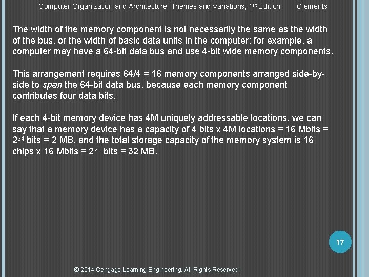
Computer Organization and Architecture: Themes and Variations, 1 st Edition Clements The width of the memory component is not necessarily the same as the width of the bus, or the width of basic data units in the computer; for example, a computer may have a 64 -bit data bus and use 4 -bit wide memory components. This arrangement requires 64/4 = 16 memory components arranged side-byside to span the 64 -bit data bus, because each memory component contributes four data bits. If each 4 -bit memory device has 4 M uniquely addressable locations, we can say that a memory device has a capacity of 4 bits x 4 M locations = 16 Mbits = 224 bits = 2 MB, and the total storage capacity of the memory system is 16 chips x 16 Mbits = 228 bits = 32 MB. 17 © 2014 Cengage Learning Engineering. All Rights Reserved.

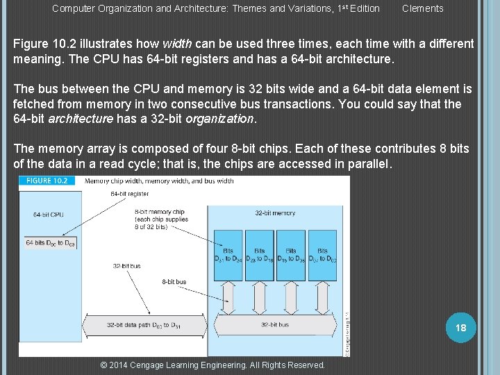
Computer Organization and Architecture: Themes and Variations, 1 st Edition Clements Figure 10. 2 illustrates how width can be used three times, each time with a different meaning. The CPU has 64 -bit registers and has a 64 -bit architecture. The bus between the CPU and memory is 32 bits wide and a 64 -bit data element is fetched from memory in two consecutive bus transactions. You could say that the 64 -bit architecture has a 32 -bit organization. The memory array is composed of four 8 -bit chips. Each of these contributes 8 bits of the data in a read cycle; that is, the chips are accessed in parallel. 18 © 2014 Cengage Learning Engineering. All Rights Reserved.

Computer Organization and Architecture: Themes and Variations, 1 st Edition Clements A memory’s principal timing parameters are its read access time, its write access time, and its cycle time. The read access time is the time taken to access a memory location and to retrieve its contents. The write access time is the time taken to write data into the device. The cycle time is the minimum period that must elapse between two consecutive memory accesses. Ideally, a memory’s read, write, and cycle times should all be the same – this is generally true for semiconductor static RAM. Some memory (e. g. , DRAM) has a longer cycle time than a read or write access because certain internal operations have to take place between consecutive accesses. We have already pointed out that read-mostly devices such as flash EPROMs have very much longer write access times than read access times. © 2014 Cengage Learning Engineering. All Rights Reserved. 19

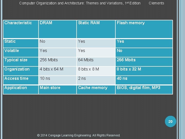
Computer Organization and Architecture: Themes and Variations, 1 st Edition Clements Characteristic DRAM Static RAM Flash memory Static No Yes Volatile Yes No Typical size 256 Mbits 64 Mbits 256 Mbits Organization 4 bits x 64 M 8 bits x 8 M 8 bits x 32 M Access time 10 ns 2 ns 40 ns Application Main store Cache memory BIOS, digital film, MP 3 20 © 2014 Cengage Learning Engineering. All Rights Reserved.

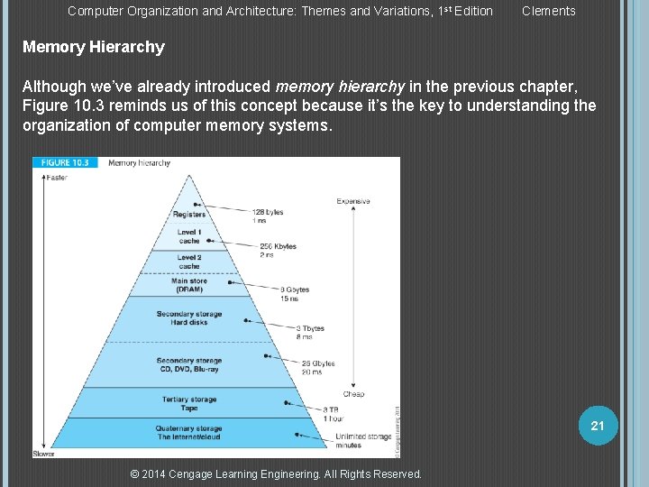
Computer Organization and Architecture: Themes and Variations, 1 st Edition Clements Memory Hierarchy Although we’ve already introduced memory hierarchy in the previous chapter, Figure 10. 3 reminds us of this concept because it’s the key to understanding the organization of computer memory systems. 21 © 2014 Cengage Learning Engineering. All Rights Reserved.

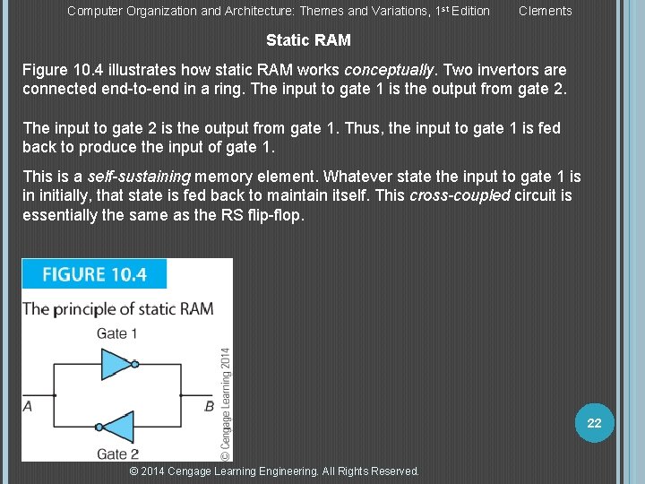
Computer Organization and Architecture: Themes and Variations, 1 st Edition Clements Static RAM Figure 10. 4 illustrates how static RAM works conceptually. Two invertors are connected end-to-end in a ring. The input to gate 1 is the output from gate 2. The input to gate 2 is the output from gate 1. Thus, the input to gate 1 is fed back to produce the input of gate 1. This is a self-sustaining memory element. Whatever state the input to gate 1 is in initially, that state is fed back to maintain itself. This cross-coupled circuit is essentially the same as the RS flip-flop. 22 © 2014 Cengage Learning Engineering. All Rights Reserved.

Computer Organization and Architecture: Themes and Variations, 1 st Edition Clements Static RAM is less important than it once was. Because of its simpler CPU interface than DRAM, it was once the memory of choice for many (particularly small) computer systems. Static RAM can retain data in a power-down mode using a small battery; a feature that was of great value before flash memory became so widely available. Today, static RAM is of less importance to the designer of large systems because of the economics of DRAM-based memories. However, because static memory can be very fast, it is still used to fabricate cache memories. As early as 1981, experimental static RAMs with access times as low as 0. 6 ns were being investigated (using gallium-arsenide rather than silicon). 23 © 2014 Cengage Learning Engineering. All Rights Reserved.

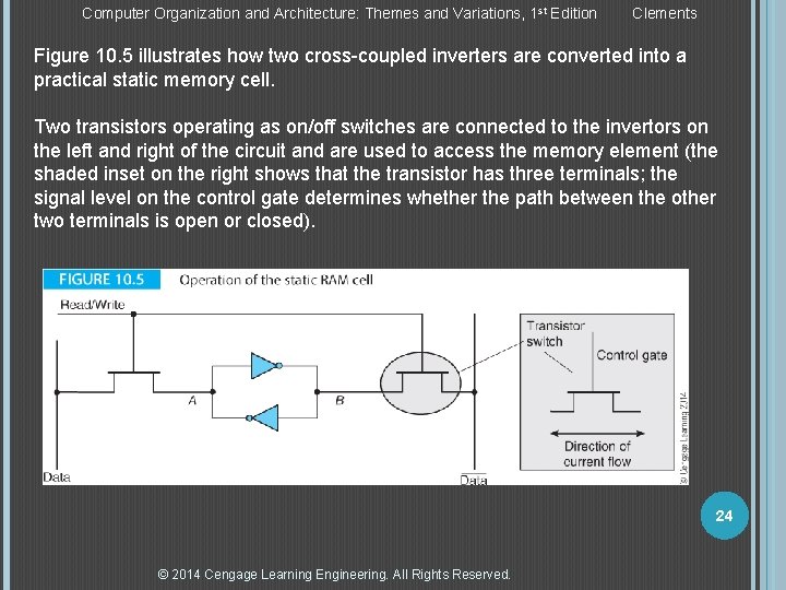
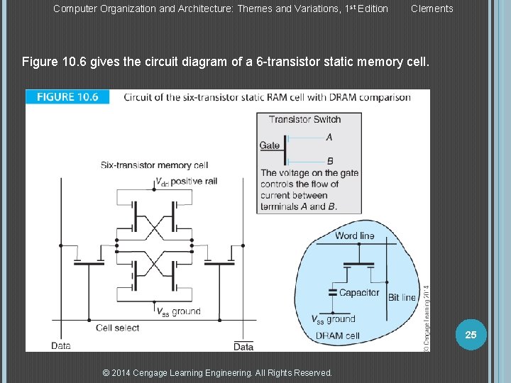
Computer Organization and Architecture: Themes and Variations, 1 st Edition Clements Figure 10. 5 illustrates how two cross-coupled inverters are converted into a practical static memory cell. Two transistors operating as on/off switches are connected to the invertors on the left and right of the circuit and are used to access the memory element (the shaded inset on the right shows that the transistor has three terminals; the signal level on the control gate determines whether the path between the other two terminals is open or closed). 24 © 2014 Cengage Learning Engineering. All Rights Reserved.

Computer Organization and Architecture: Themes and Variations, 1 st Edition Clements Figure 10. 6 gives the circuit diagram of a 6 -transistor static memory cell. 25 © 2014 Cengage Learning Engineering. All Rights Reserved.

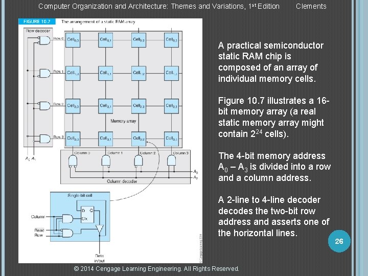
Computer Organization and Architecture: Themes and Variations, 1 st Edition Clements A practical semiconductor static RAM chip is composed of an array of individual memory cells. Figure 10. 7 illustrates a 16 bit memory array (a real static memory array might contain 224 cells). The 4 -bit memory address A 0 – A 3 is divided into a row and a column address. A 2 -line to 4 -line decoder decodes the two-bit row address and asserts one of the horizontal lines. © 2014 Cengage Learning Engineering. All Rights Reserved. 26

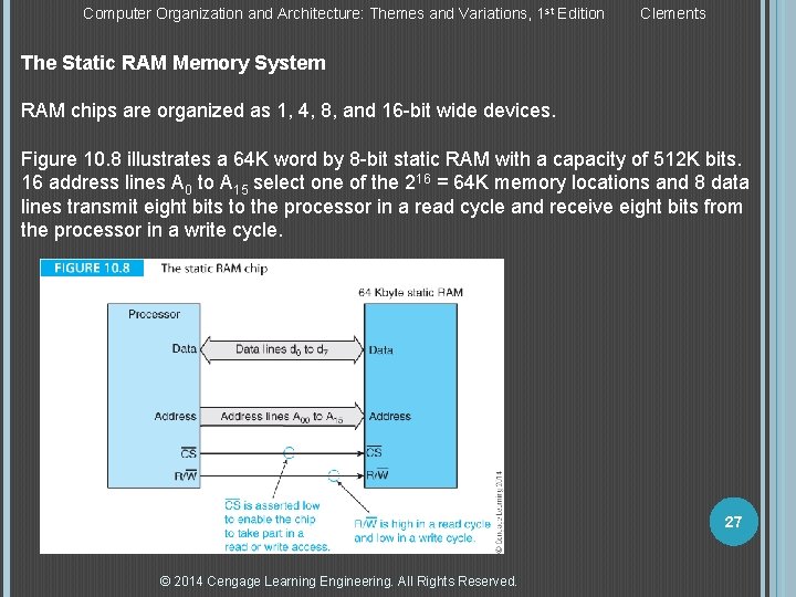
Computer Organization and Architecture: Themes and Variations, 1 st Edition Clements The Static RAM Memory System RAM chips are organized as 1, 4, 8, and 16 -bit wide devices. Figure 10. 8 illustrates a 64 K word by 8 -bit static RAM with a capacity of 512 K bits. 16 address lines A 0 to A 15 select one of the 216 = 64 K memory locations and 8 data lines transmit eight bits to the processor in a read cycle and receive eight bits from the processor in a write cycle. 27 © 2014 Cengage Learning Engineering. All Rights Reserved.

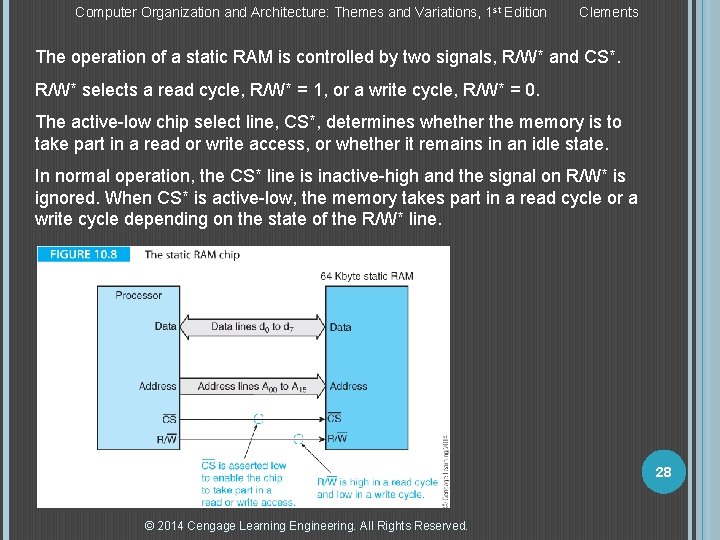
Computer Organization and Architecture: Themes and Variations, 1 st Edition Clements The operation of a static RAM is controlled by two signals, R/W* and CS*. R/W* selects a read cycle, R/W* = 1, or a write cycle, R/W* = 0. The active-low chip select line, CS*, determines whether the memory is to take part in a read or write access, or whether it remains in an idle state. In normal operation, the CS* line is inactive-high and the signal on R/W* is ignored. When CS* is active-low, the memory takes part in a read cycle or a write cycle depending on the state of the R/W* line. 28 © 2014 Cengage Learning Engineering. All Rights Reserved.

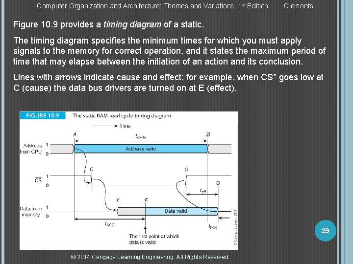
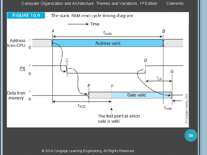
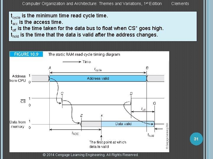
Computer Organization and Architecture: Themes and Variations, 1 st Edition Clements Figure 10. 9 provides a timing diagram of a static. The timing diagram specifies the minimum times for which you must apply signals to the memory for correct operation, and it states the maximum period of time that may elapse between the initiation of an action and its conclusion. Lines with arrows indicate cause and effect; for example, when CS* goes low at C (cause) the data bus drivers are turned on at E (effect). 29 © 2014 Cengage Learning Engineering. All Rights Reserved.

Computer Organization and Architecture: Themes and Variations, 1 st Edition Clements 30 © 2014 Cengage Learning Engineering. All Rights Reserved.

Computer Organization and Architecture: Themes and Variations, 1 st Edition Clements tcycle is the minimum time read cycle time. tacc is the access time. toff is the time taken for the data bus to float when CS* goes high. thold is the time that the data is valid after the address changes. 31 © 2014 Cengage Learning Engineering. All Rights Reserved.

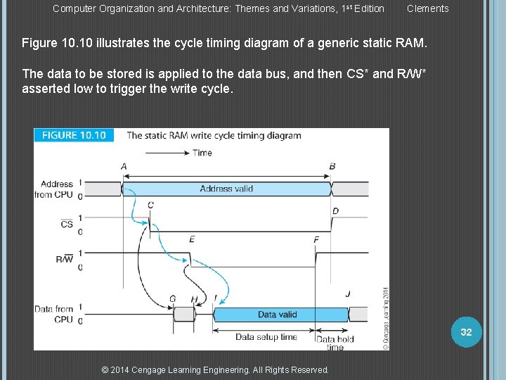
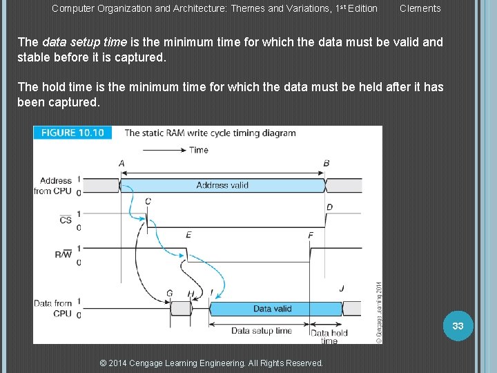
Computer Organization and Architecture: Themes and Variations, 1 st Edition Clements Figure 10. 10 illustrates the cycle timing diagram of a generic static RAM. The data to be stored is applied to the data bus, and then CS* and R/W* asserted low to trigger the write cycle. 32 © 2014 Cengage Learning Engineering. All Rights Reserved.

Computer Organization and Architecture: Themes and Variations, 1 st Edition Clements The data setup time is the minimum time for which the data must be valid and stable before it is captured. The hold time is the minimum time for which the data must be held after it has been captured. 33 © 2014 Cengage Learning Engineering. All Rights Reserved.

Computer Organization and Architecture: Themes and Variations, 1 st Edition Clements Byte/Word Control In the 1970 s microprocessors were byte-oriented and data buses were eight bits wide. Address buses were 16 bits wide and an address on A 15 to A 00 selected one of 216 = 64 K unique bytes. When 16 -bit processors were introduced, the situation became more complex because of the need to access both bytes and 16 -bit words (remember that memory is byte-addressed and you can access an individual byte even though the fundamental wordlength may be two, four, or more bytes). Because microprocessor designers wanted the best of both worlds, the ability to access individual bytes as well as 16 -bit words, they implemented byte-control mechanisms allowing access to the individual bytes of a selected word. A typical mechanism uses the address bus to select a 16 -bit word (or a 32 -bit or a 64 -bit) word and then uses byte control lines to select one or more of the bytes at that address. 34 © 2014 Cengage Learning Engineering. All Rights Reserved.

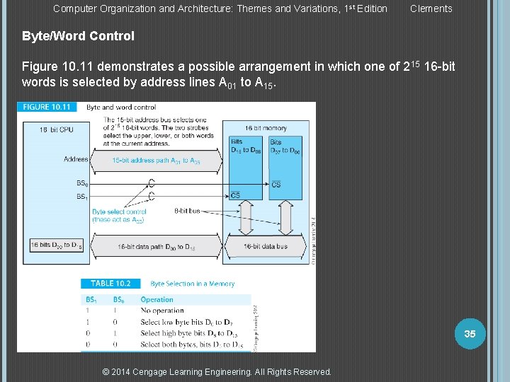
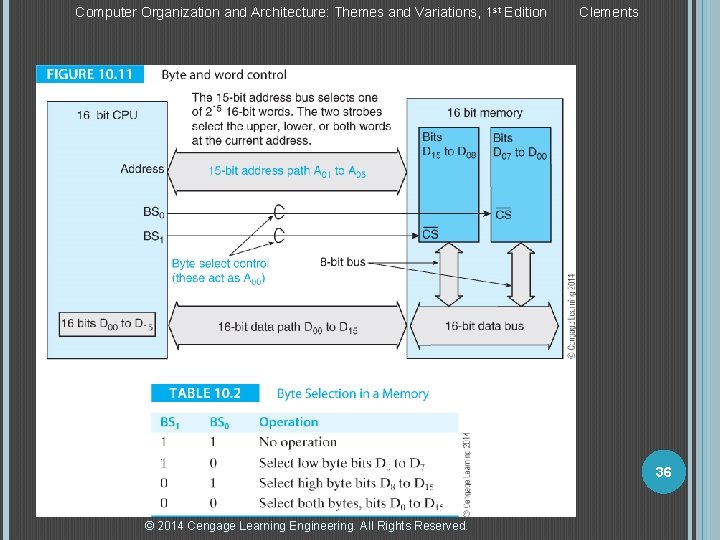
Computer Organization and Architecture: Themes and Variations, 1 st Edition Clements Byte/Word Control Figure 10. 11 demonstrates a possible arrangement in which one of 215 16 -bit words is selected by address lines A 01 to A 15. 35 © 2014 Cengage Learning Engineering. All Rights Reserved.

Computer Organization and Architecture: Themes and Variations, 1 st Edition Clements 36 © 2014 Cengage Learning Engineering. All Rights Reserved.

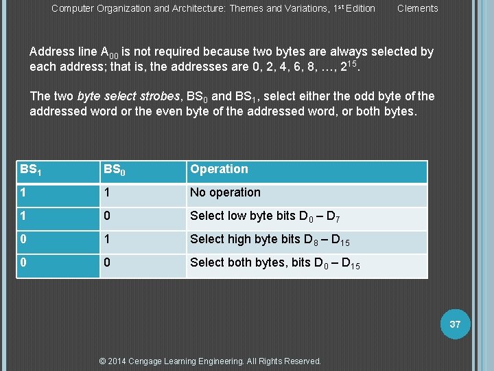
Computer Organization and Architecture: Themes and Variations, 1 st Edition Clements Address line A 00 is not required because two bytes are always selected by each address; that is, the addresses are 0, 2, 4, 6, 8, …, 215. The two byte select strobes, BS 0 and BS 1, select either the odd byte of the addressed word or the even byte of the addressed word, or both bytes. BS 1 BS 0 Operation 1 1 No operation 1 0 Select low byte bits D 0 – D 7 0 1 Select high byte bits D 8 – D 15 0 0 Select both bytes, bits D 0 – D 15 37 © 2014 Cengage Learning Engineering. All Rights Reserved.

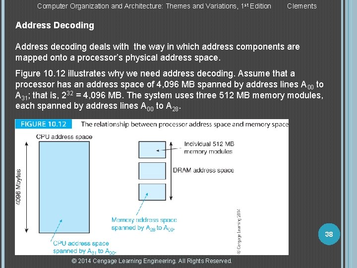
Computer Organization and Architecture: Themes and Variations, 1 st Edition Clements Address Decoding Address decoding deals with the way in which address components are mapped onto a processor’s physical address space. Figure 10. 12 illustrates why we need address decoding. Assume that a processor has an address space of 4, 096 MB spanned by address lines A 00 to A 31; that is, 232 = 4, 096 MB. The system uses three 512 MB memory modules, each spanned by address lines A 00 to A 28. 38 © 2014 Cengage Learning Engineering. All Rights Reserved.

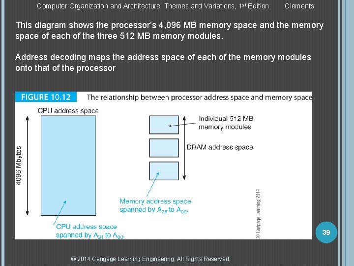
Computer Organization and Architecture: Themes and Variations, 1 st Edition Clements This diagram shows the processor’s 4, 096 MB memory space and the memory space of each of the three 512 MB memory modules. Address decoding maps the address space of each of the memory modules onto that of the processor 39 © 2014 Cengage Learning Engineering. All Rights Reserved.

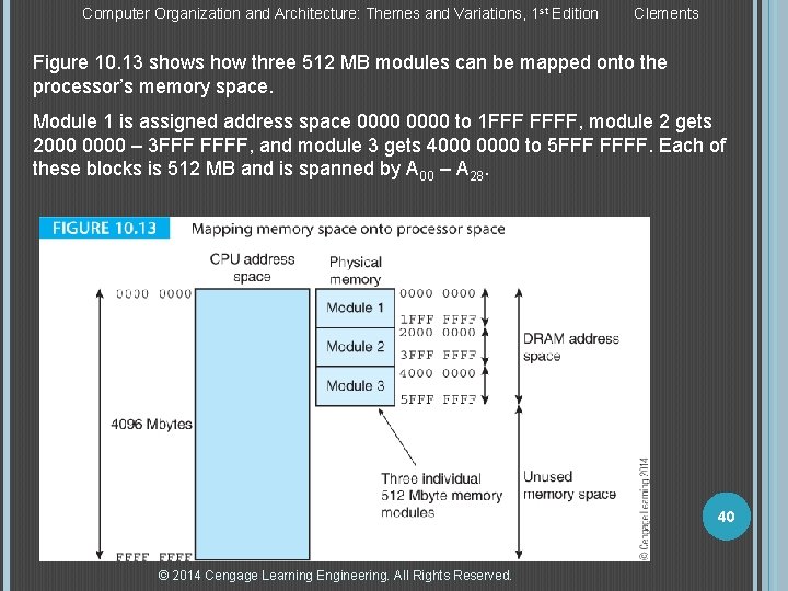
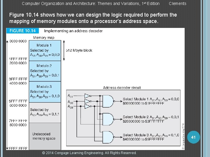
Computer Organization and Architecture: Themes and Variations, 1 st Edition Clements Figure 10. 13 shows how three 512 MB modules can be mapped onto the processor’s memory space. Module 1 is assigned address space 0000 to 1 FFF FFFF, module 2 gets 2000 0000 – 3 FFF FFFF, and module 3 gets 4000 0000 to 5 FFF FFFF. Each of these blocks is 512 MB and is spanned by A 00 – A 28. 40 © 2014 Cengage Learning Engineering. All Rights Reserved.

Computer Organization and Architecture: Themes and Variations, 1 st Edition Clements Figure 10. 14 shows how we can design the logic required to perform the mapping of memory modules onto a processor’s address space. 41 © 2014 Cengage Learning Engineering. All Rights Reserved.

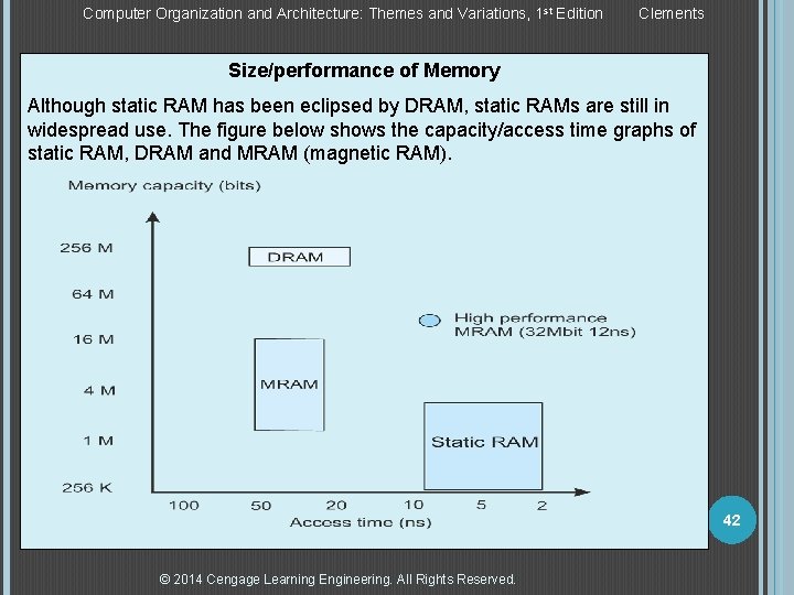
Computer Organization and Architecture: Themes and Variations, 1 st Edition Clements Size/performance of Memory Although static RAM has been eclipsed by DRAM, static RAMs are still in widespread use. The figure below shows the capacity/access time graphs of static RAM, DRAM and MRAM (magnetic RAM). 42 © 2014 Cengage Learning Engineering. All Rights Reserved.

Computer Organization and Architecture: Themes and Variations, 1 st Edition Clements Interleaved Memory If you have a memory system with an access time of tacc, there’s nothing you can do to reduce that access time. You can reduce the effective access time by interleaving. If a memory location is accessed at time T 0, the data becomes available tacc seconds later. Another location in the same memory can’t be accessed until at least tacc has elapsed. But, you can access a different module at any time; that is, you access multiple parallel memories in parallel. 43 © 2014 Cengage Learning Engineering. All Rights Reserved.

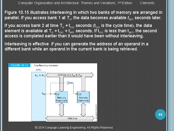
Computer Organization and Architecture: Themes and Variations, 1 st Edition Clements Figure 10. 15 illustrates interleaving in which two banks of memory are arranged in parallel. If you access bank 1 at To, the data becomes available tacc seconds later. If you access bank 2 at time To + tcyc seconds (tcyc is the cycle time), the data element is available at To + tcyc + tacc seconds. If tcyc is less than tacc, the second access is completed earlier than it would have been without interleaving. Interleaving is effective if you can generate the address of an operand in a different bank while an operand in the current bank is being retrieved. 44 © 2014 Cengage Learning Engineering. All Rights Reserved.

Computer Organization and Architecture: Themes and Variations, 1 st Edition Clements DRAM History DRAM is just a little older than the microprocessor itself. Indeed, the world’s first commercial DRAM chip was Intel’s 1103 1024 -bit memory. The concept of the one-bit dynamic memory cell using a single transistor dates back to R. H. Denning’s work at IBM in 1966. The first DRAM was fabricated with PMOS (positive channel metal oxide semiconductor) technology that is now obsolete. A few years later, 4 K-bit DRAMs were built with NMOS (negative channel metal oxide semiconductor) technology. The introduction of CMOS (complementary metal oxide semiconductor) technology was a breakthrough because of its much reduced power consumption. DRAMs still use CMOS technology. 45 © 2014 Cengage Learning Engineering. All Rights Reserved.

Computer Organization and Architecture: Themes and Variations, 1 st Edition Clements DRAM Most PCs and workstations implement their main memories with DRAM which has played a key role in the development of high-performance computers and its operating parameters are continually changing as new variants are developed. An understanding of DRAM is necessary to appreciate where computers are heading in the near future. We begin this section by describing the DRAM’s operating principles, look at its timing requirements, introduce the DRAM family, and then describe how they are used in PCs. 46 © 2014 Cengage Learning Engineering. All Rights Reserved.

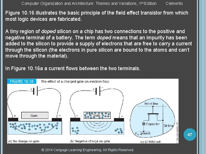
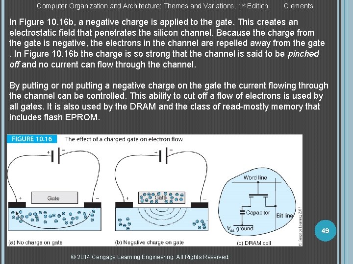
Computer Organization and Architecture: Themes and Variations, 1 st Edition Clements Figure 10. 16 illustrates the basic principle of the field effect transistor from which most logic devices are fabricated. A tiny region of doped silicon on a chip has two connections to the positive and negative terminal of a battery. The term doped means that an impurity has been added to the silicon to provide a supply of electrons that are free to carry a current through the silicon (the electrons in pure silicon are bound to the atoms and can’t move through the material). In Figure 10. 16 a a current flows between the two terminals. 47 © 2014 Cengage Learning Engineering. All Rights Reserved.

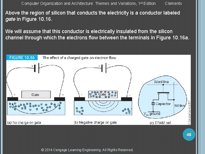
Computer Organization and Architecture: Themes and Variations, 1 st Edition Clements Above the region of silicon that conducts the electricity is a conductor labeled gate in Figure 10. 16. We will assume that this conductor is electrically insulated from the silicon channel through which the electrons flow between the terminals in Figure 10. 16 a. 48 © 2014 Cengage Learning Engineering. All Rights Reserved.

Computer Organization and Architecture: Themes and Variations, 1 st Edition Clements In Figure 10. 16 b, a negative charge is applied to the gate. This creates an electrostatic field that penetrates the silicon channel. Because the charge from the gate is negative, the electrons in the channel are repelled away from the gate. In Figure 10. 16 b the charge is so strong that the channel is said to be pinched off and no current can flow through the channel. By putting or not putting a negative charge on the gate the current flowing through the channel can be controlled. This ability to cut off a flow of electrons is used by all gates. It is also used by the DRAM and the class of read-mostly memory that includes flash EPROM. 49 © 2014 Cengage Learning Engineering. All Rights Reserved.

Computer Organization and Architecture: Themes and Variations, 1 st Edition Clements Suppose we apply a negative voltage to the gate of a transistor in order to place a charge on the gate and turn the transistor off. If the voltage is removed, the transistor does not begin to conduct again until the charge is dissipated. If the gate is insulated from the channel, the time taken to dissipate the charge may be several milliseconds. The effect of a stored charge on a capacitor forms the basis of the singletransistor DRAM cell. A charge is applied to a gate to place the transistor in one of two states. Figure 10. 6(c) illustrates the structure of a single-transistor DRAM cell. This stored charge eventually leaks away and any data stored in the cell is lost leaving all cells in the same state. In order to exploit the memory effect of a stored charge, a practical memory has to read the state of the transistor every few milliseconds and then rewrite the charge back into the transistor. This operation is called refreshing. 50 © 2014 Cengage Learning Engineering. All Rights Reserved.

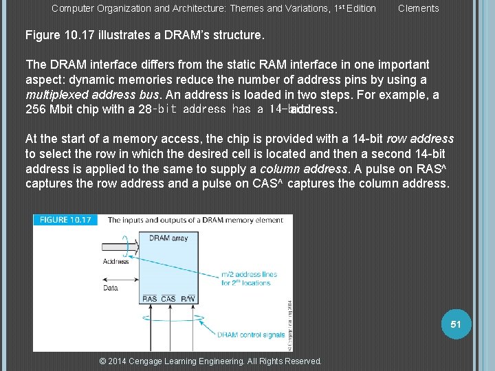
Computer Organization and Architecture: Themes and Variations, 1 st Edition Clements Figure 10. 17 illustrates a DRAM’s structure. The DRAM interface differs from the static RAM interface in one important aspect: dynamic memories reduce the number of address pins by using a multiplexed address bus. An address is loaded in two steps. For example, a 256 Mbit chip with a 28‑bit address has a 14 -bit address. At the start of a memory access, the chip is provided with a 14 -bit row address to select the row in which the desired cell is located and then a second 14 -bit address is applied to the same to supply a column address. A pulse on RAS^ captures the row address and a pulse on CAS^ captures the column address. 51 © 2014 Cengage Learning Engineering. All Rights Reserved.

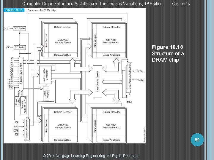
Computer Organization and Architecture: Themes and Variations, 1 st Edition Clements Figure 10. 18 Structure of a DRAM chip 52 © 2014 Cengage Learning Engineering. All Rights Reserved.

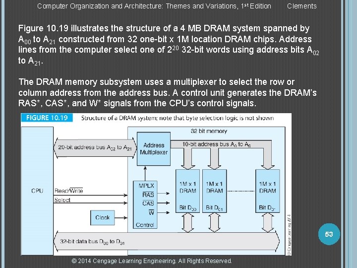
Computer Organization and Architecture: Themes and Variations, 1 st Edition Clements Figure 10. 19 illustrates the structure of a 4 MB DRAM system spanned by A 00 to A 21 constructed from 32 one-bit x 1 M location DRAM chips. Address lines from the computer select one of 220 32 -bit words using address bits A 02 to A 21. The DRAM memory subsystem uses a multiplexer to select the row or column address from the address bus. A control unit generates the DRAM’s RAS*, CAS*, and W* signals from the CPU’s control signals. 53 © 2014 Cengage Learning Engineering. All Rights Reserved.

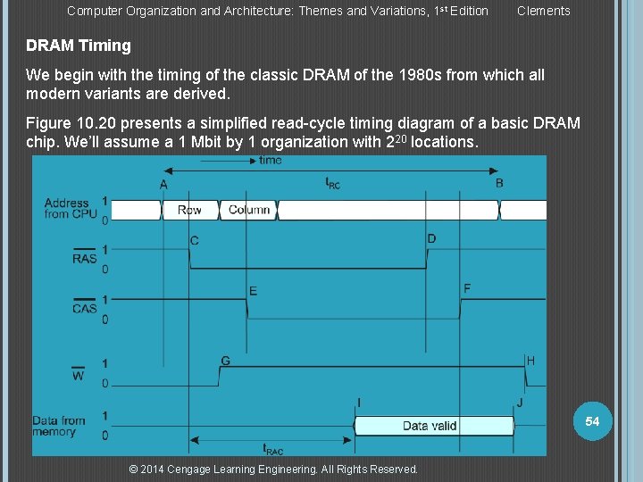
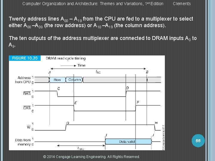
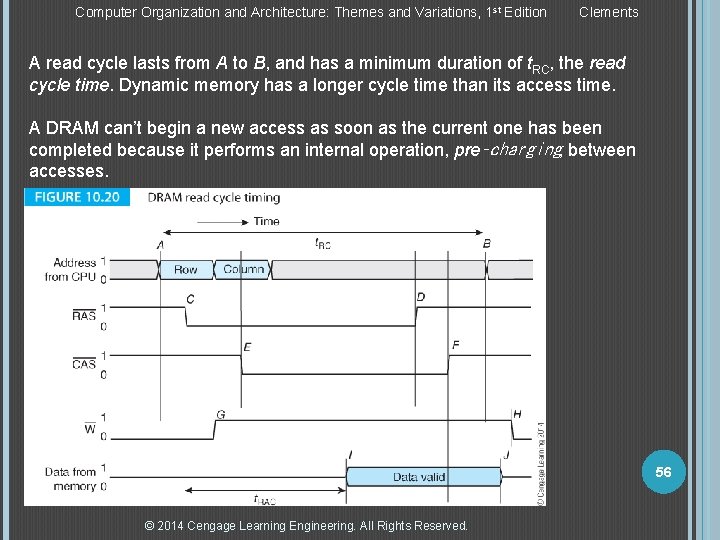
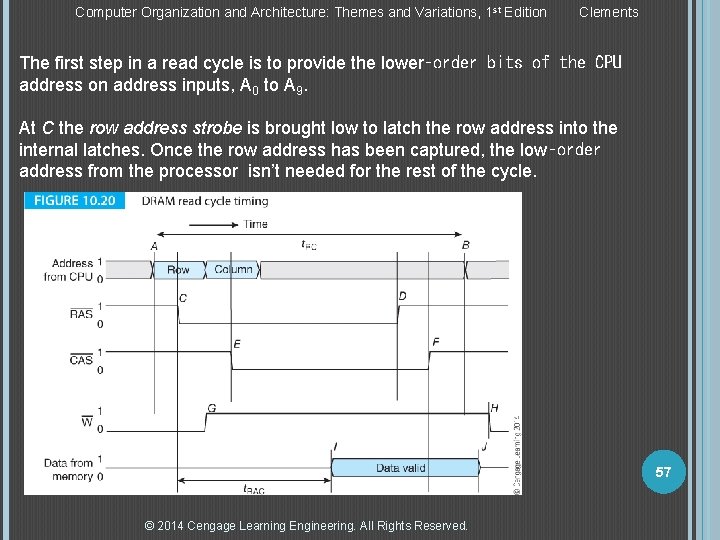
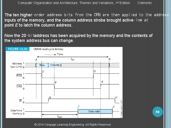
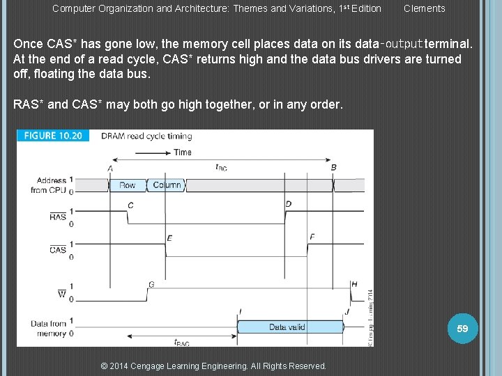
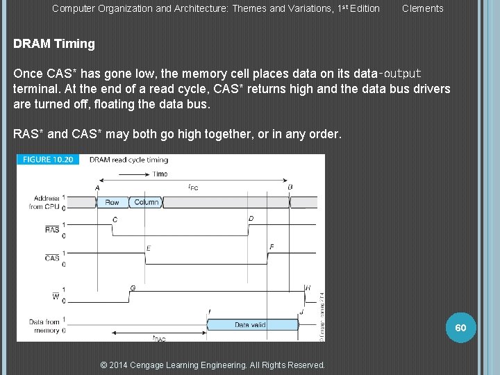
Computer Organization and Architecture: Themes and Variations, 1 st Edition Clements DRAM Timing We begin with the timing of the classic DRAM of the 1980 s from which all modern variants are derived. Figure 10. 20 presents a simplified read-cycle timing diagram of a basic DRAM chip. We’ll assume a 1 Mbit by 1 organization with 220 locations. 54 © 2014 Cengage Learning Engineering. All Rights Reserved.

Computer Organization and Architecture: Themes and Variations, 1 st Edition Clements Twenty address lines A 00 – A 19 from the CPU are fed to a multiplexer to select either A 00 –A 09 (the row address) or A 10 –A 19 (the column address). The ten outputs of the address multiplexer are connected to DRAM inputs A 0 to A 9. 55 © 2014 Cengage Learning Engineering. All Rights Reserved.

Computer Organization and Architecture: Themes and Variations, 1 st Edition Clements A read cycle lasts from A to B, and has a minimum duration of t. RC, the read cycle time. Dynamic memory has a longer cycle time than its access time. A DRAM can’t begin a new access as soon as the current one has been completed because it performs an internal operation, pre‑charging, between accesses. 56 © 2014 Cengage Learning Engineering. All Rights Reserved.

Computer Organization and Architecture: Themes and Variations, 1 st Edition Clements The first step in a read cycle is to provide the lower‑order bits of the CPU address on address inputs, A 0 to A 9. At C the row address strobe is brought low to latch the row address into the internal latches. Once the row address has been captured, the low‑order address from the processor isn’t needed for the rest of the cycle. 57 © 2014 Cengage Learning Engineering. All Rights Reserved.

Computer Organization and Architecture: Themes and Variations, 1 st Edition Clements The ten higher‑order address bits from the CPU are then applied to the address inputs of the memory, and the column address strobe brought active‑low at point E to latch the column address. Now the 20‑bitaddress has been acquired by the memory and the contents of the system address bus can change. 58 © 2014 Cengage Learning Engineering. All Rights Reserved.

Computer Organization and Architecture: Themes and Variations, 1 st Edition Clements Once CAS* has gone low, the memory cell places data on its data‑output terminal. At the end of a read cycle, CAS* returns high and the data bus drivers are turned off, floating the data bus. RAS* and CAS* may both go high together, or in any order. 59 © 2014 Cengage Learning Engineering. All Rights Reserved.

Computer Organization and Architecture: Themes and Variations, 1 st Edition Clements DRAM Timing Once CAS* has gone low, the memory cell places data on its data‑output terminal. At the end of a read cycle, CAS* returns high and the data bus drivers are turned off, floating the data bus. RAS* and CAS* may both go high together, or in any order. 60 © 2014 Cengage Learning Engineering. All Rights Reserved.

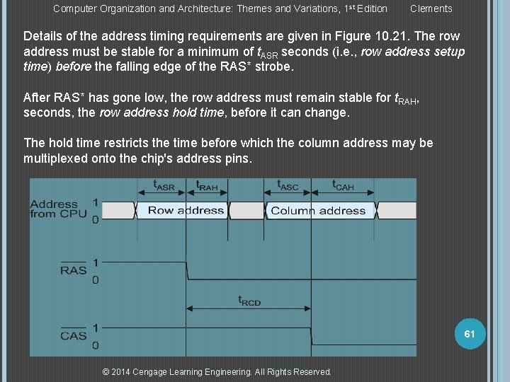
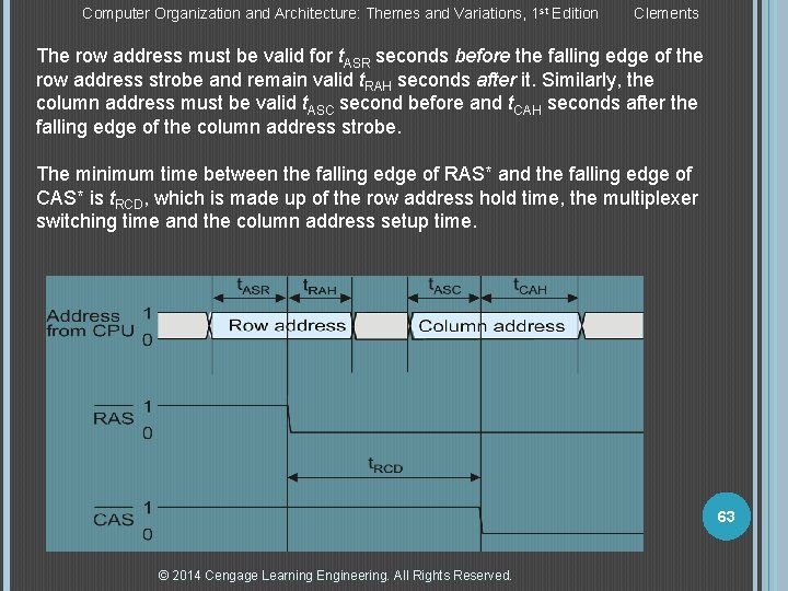
Computer Organization and Architecture: Themes and Variations, 1 st Edition Clements Details of the address timing requirements are given in Figure 10. 21. The row address must be stable for a minimum of t. ASR seconds (i. e. , row address setup time) before the falling edge of the RAS* strobe. After RAS* has gone low, the row address must remain stable for t. RAH, seconds, the row address hold time, before it can change. The hold time restricts the time before which the column address may be multiplexed onto the chip's address pins. 61 © 2014 Cengage Learning Engineering. All Rights Reserved.

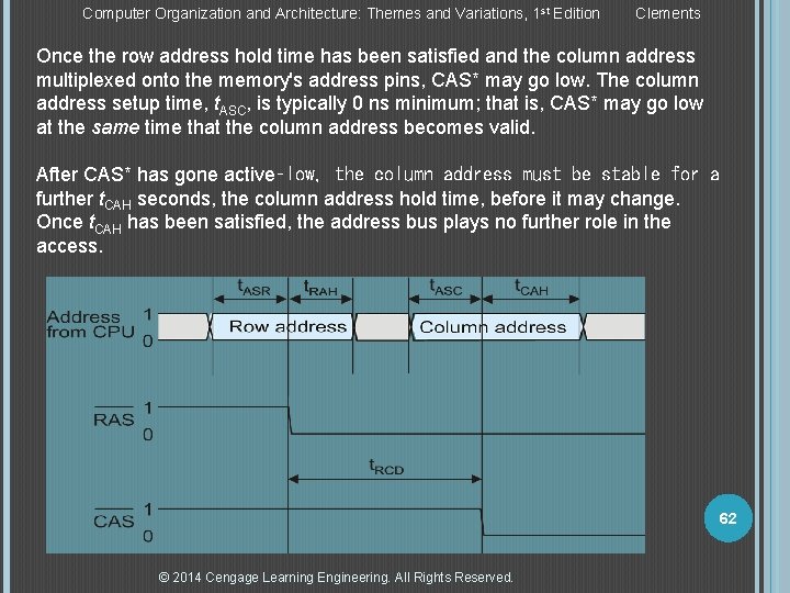
Computer Organization and Architecture: Themes and Variations, 1 st Edition Clements Once the row address hold time has been satisfied and the column address multiplexed onto the memory's address pins, CAS* may go low. The column address setup time, t. ASC, is typically 0 ns minimum; that is, CAS* may go low at the same time that the column address becomes valid. After CAS* has gone active‑low, the column address must be stable for a further t. CAH seconds, the column address hold time, before it may change. Once t. CAH has been satisfied, the address bus plays no further role in the access. 62 © 2014 Cengage Learning Engineering. All Rights Reserved.

Computer Organization and Architecture: Themes and Variations, 1 st Edition Clements The row address must be valid for t. ASR seconds before the falling edge of the row address strobe and remain valid t. RAH seconds after it. Similarly, the column address must be valid t. ASC second before and t. CAH seconds after the falling edge of the column address strobe. The minimum time between the falling edge of RAS* and the falling edge of CAS* is t. RCD, which is made up of the row address hold time, the multiplexer switching time and the column address setup time. 63 © 2014 Cengage Learning Engineering. All Rights Reserved.

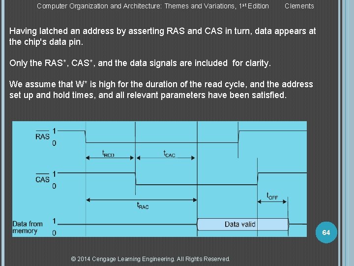
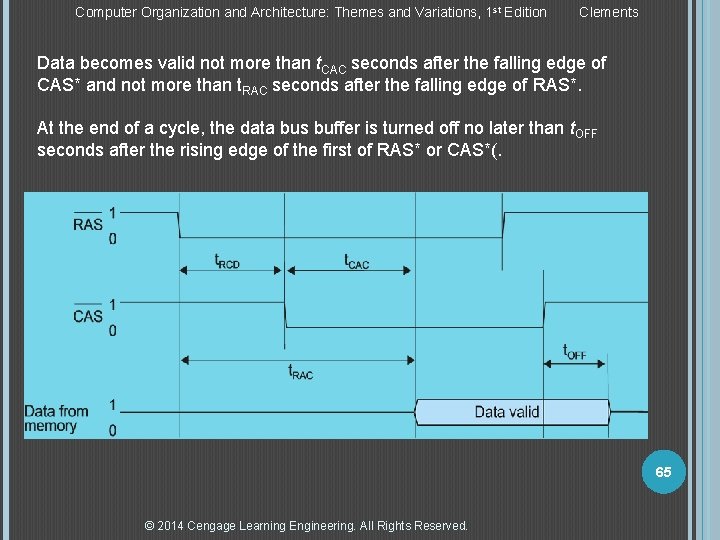
Computer Organization and Architecture: Themes and Variations, 1 st Edition Clements Having latched an address by asserting RAS and CAS in turn, data appears at the chip's data pin. Only the RAS*, CAS*, and the data signals are included for clarity. We assume that W* is high for the duration of the read cycle, and the address set up and hold times, and all relevant parameters have been satisfied. 64 © 2014 Cengage Learning Engineering. All Rights Reserved.

Computer Organization and Architecture: Themes and Variations, 1 st Edition Clements Data becomes valid not more than t. CAC seconds after the falling edge of CAS* and not more than t. RAC seconds after the falling edge of RAS*. At the end of a cycle, the data bus buffer is turned off no later than t. OFF seconds after the rising edge of the first of RAS* or CAS*(. 65 © 2014 Cengage Learning Engineering. All Rights Reserved.

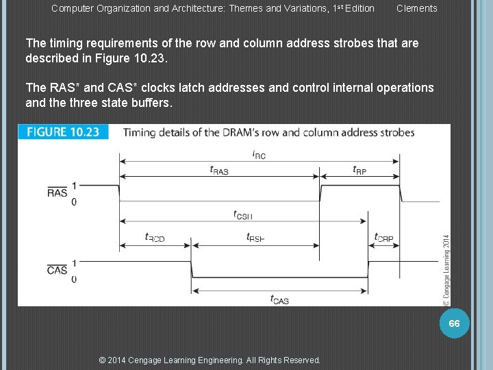
Computer Organization and Architecture: Themes and Variations, 1 st Edition Clements The timing requirements of the row and column address strobes that are described in Figure 10. 23. The RAS* and CAS* clocks latch addresses and control internal operations and the three state buffers. 66 © 2014 Cengage Learning Engineering. All Rights Reserved.

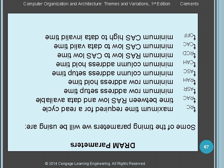
© 2014 Cengage Learning Engineering. All Rights Reserved. 67 DRAM Parameters Some of the timing parameters we will be using are: t. RC t. RAC t. ASR t. RAH t. ASC t. CAH t. RCD t. CAC t. OFF maximum time required for a read cycle time between RAS low and data available minimum row address setup time minimum row address hold time minimum column address setup time minimum column address hold time minimum RAS low to CAS low time minimum CAS low to data valid time minimum CAS high to data invalid time Computer Organization and Architecture: Themes and Variations, 1 st Edition Clements

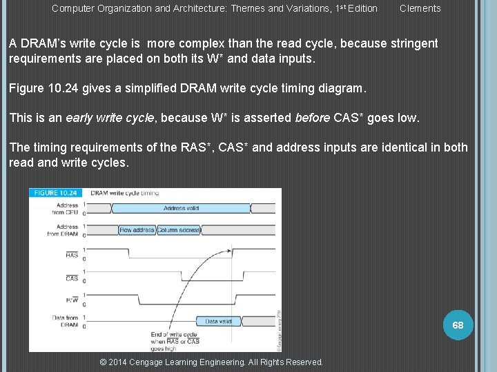
Computer Organization and Architecture: Themes and Variations, 1 st Edition Clements A DRAM’s write cycle is more complex than the read cycle, because stringent requirements are placed on both its W* and data inputs. Figure 10. 24 gives a simplified DRAM write cycle timing diagram. This is an early write cycle, because W* is asserted before CAS* goes low. The timing requirements of the RAS*, CAS* and address inputs are identical in both read and write cycles. 68 © 2014 Cengage Learning Engineering. All Rights Reserved.

Computer Organization and Architecture: Themes and Variations, 1 st Edition Clements Theme and Variations on DRAM We’ve now described the plain vanilla DRAM. Next we look at the successive generations of improved DRAMs starting with the page, nibble and static column modes. These variations exploit the way in which the address input is multiplexed between rows and columns and overcome some of the limitations caused by precharging between accesses. 69 © 2014 Cengage Learning Engineering. All Rights Reserved.

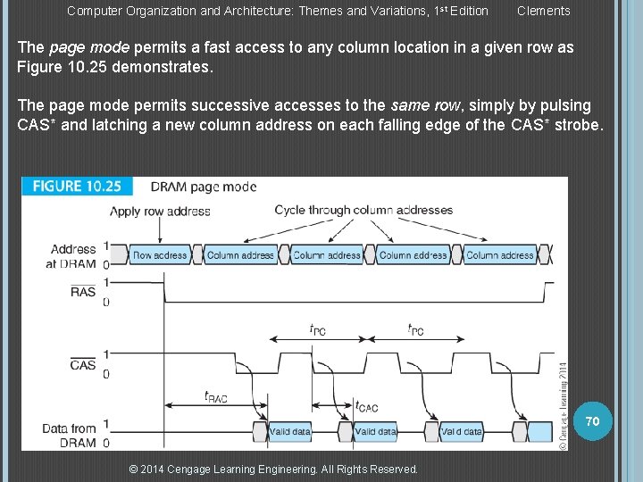
Computer Organization and Architecture: Themes and Variations, 1 st Edition Clements The page mode permits a fast access to any column location in a given row as Figure 10. 25 demonstrates. The page mode permits successive accesses to the same row, simply by pulsing CAS* and latching a new column address on each falling edge of the CAS* strobe. 70 © 2014 Cengage Learning Engineering. All Rights Reserved.

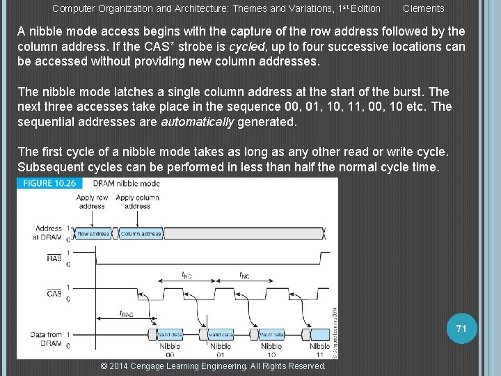
Computer Organization and Architecture: Themes and Variations, 1 st Edition Clements A nibble mode access begins with the capture of the row address followed by the column address. If the CAS* strobe is cycled, up to four successive locations can be accessed without providing new column addresses. The nibble mode latches a single column address at the start of the burst. The next three accesses take place in the sequence 00, 01, 10, 11, 00, 10 etc. The sequential addresses are automatically generated. The first cycle of a nibble mode takes as long as any other read or write cycle. Subsequent cycles can be performed in less than half the normal cycle time. 71 © 2014 Cengage Learning Engineering. All Rights Reserved.

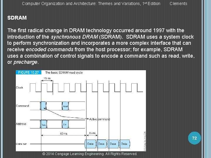
Computer Organization and Architecture: Themes and Variations, 1 st Edition Clements SDRAM The first radical change in DRAM technology occurred around 1997 with the introduction of the synchronous DRAM (SDRAM). SDRAM uses a system clock to perform synchronization and incorporates a more complex interface that can receive encoded commands from the host processor; for example, SDRAM uses a combination of control signals to encode a command such as read, write, or precharge. 72 © 2014 Cengage Learning Engineering. All Rights Reserved.

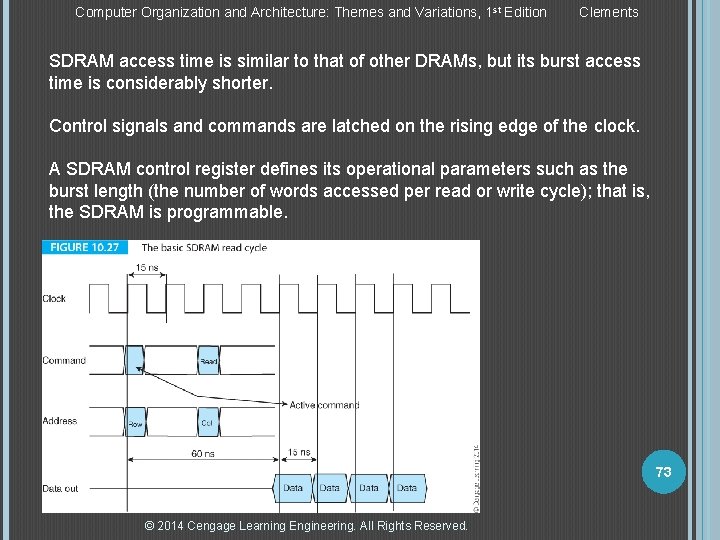
Computer Organization and Architecture: Themes and Variations, 1 st Edition Clements SDRAM access time is similar to that of other DRAMs, but its burst access time is considerably shorter. Control signals and commands are latched on the rising edge of the clock. A SDRAM control register defines its operational parameters such as the burst length (the number of words accessed per read or write cycle); that is, the SDRAM is programmable. 73 © 2014 Cengage Learning Engineering. All Rights Reserved.

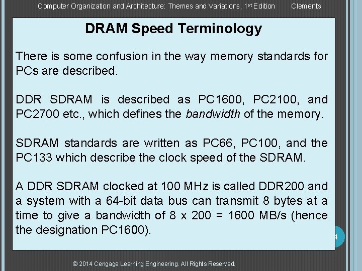
Computer Organization and Architecture: Themes and Variations, 1 st Edition Clements DRAM Speed Terminology There is some confusion in the way memory standards for PCs are described. DDR SDRAM is described as PC 1600, PC 2100, and PC 2700 etc. , which defines the bandwidth of the memory. SDRAM standards are written as PC 66, PC 100, and the PC 133 which describe the clock speed of the SDRAM. A DDR SDRAM clocked at 100 MHz is called DDR 200 and a system with a 64 -bit data bus can transmit 8 bytes at a time to give a bandwidth of 8 x 200 = 1600 MB/s (hence the designation PC 1600). 74 © 2014 Cengage Learning Engineering. All Rights Reserved.

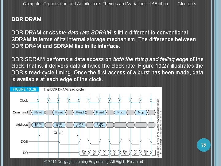
Computer Organization and Architecture: Themes and Variations, 1 st Edition Clements DDR DRAM or double-data rate SDRAM is little different to conventional SDRAM in terms of its internal storage mechanism. The difference between DDR DRAM and SDRAM lies in its interface. DDR SDRAM performs a data access on both the rising and falling edge of the clock; that is, it delivers data at twice the clock rate. Figure 10. 27 illustrates the DDR’s read-cycle timing. Once the first access of a burst has been made, data is available at each edge of the clock. 75 © 2014 Cengage Learning Engineering. All Rights Reserved.

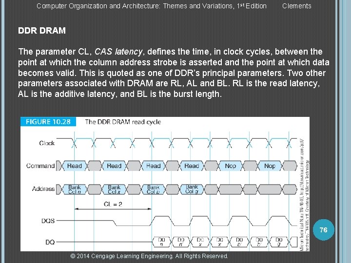
Computer Organization and Architecture: Themes and Variations, 1 st Edition Clements DDR DRAM The parameter CL, CAS latency, defines the time, in clock cycles, between the point at which the column address strobe is asserted and the point at which data becomes valid. This is quoted as one of DDR’s principal parameters. Two other parameters associated with DRAM are RL, AL and BL. RL is the read latency, AL is the additive latency, and BL is the burst length. 76 © 2014 Cengage Learning Engineering. All Rights Reserved.

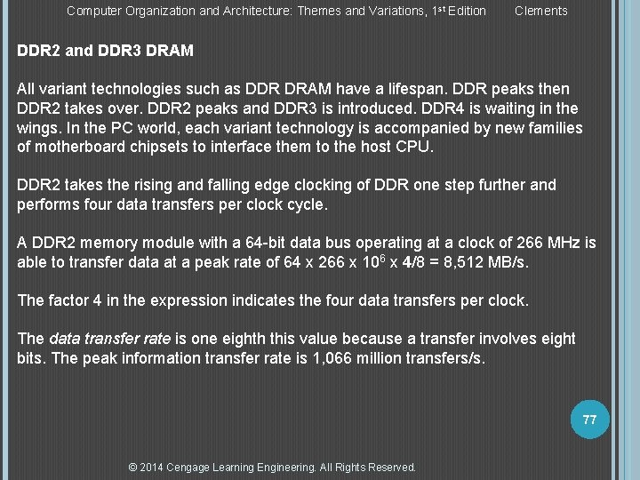
Computer Organization and Architecture: Themes and Variations, 1 st Edition Clements DDR 2 and DDR 3 DRAM All variant technologies such as DDR DRAM have a lifespan. DDR peaks then DDR 2 takes over. DDR 2 peaks and DDR 3 is introduced. DDR 4 is waiting in the wings. In the PC world, each variant technology is accompanied by new families of motherboard chipsets to interface them to the host CPU. DDR 2 takes the rising and falling edge clocking of DDR one step further and performs four data transfers per clock cycle. A DDR 2 memory module with a 64 -bit data bus operating at a clock of 266 MHz is able to transfer data at a peak rate of 64 x 266 x 106 x 4/8 = 8, 512 MB/s. The factor 4 in the expression indicates the four data transfers per clock. The data transfer rate is one eighth this value because a transfer involves eight bits. The peak information transfer rate is 1, 066 million transfers/s. 77 © 2014 Cengage Learning Engineering. All Rights Reserved.

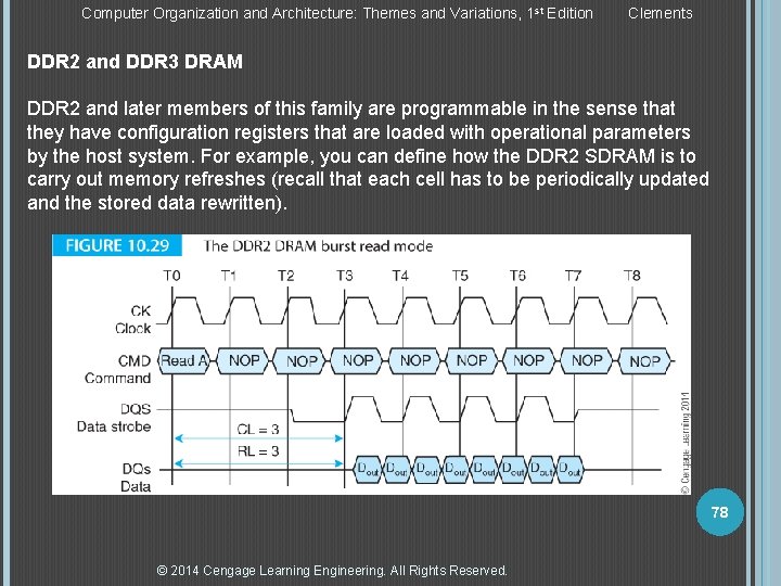
Computer Organization and Architecture: Themes and Variations, 1 st Edition Clements DDR 2 and DDR 3 DRAM DDR 2 and later members of this family are programmable in the sense that they have configuration registers that are loaded with operational parameters by the host system. For example, you can define how the DDR 2 SDRAM is to carry out memory refreshes (recall that each cell has to be periodically updated and the stored data rewritten). 78 © 2014 Cengage Learning Engineering. All Rights Reserved.

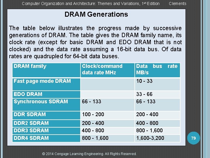
Computer Organization and Architecture: Themes and Variations, 1 st Edition Clements DRAM Generations The table below illustrates the progress made by successive generations of DRAM. The table gives the DRAM family name, its clock rate (except for basic DRAM and EDO DRAM that is not clocked) and the data rate assuming a 16 -bit data bus. Of data rates are quadrupled for 64 -bit data buses. DRAM family Clock/command data rate MHz Data bus MB/s Fast page mode DRAM 10 - 33 EDO DRAM Synchronous SDRAM 66 - 133 33 - 66 66 - 133 DDR SDRAM 100 - 200 - 400 DDR 2 SDRAM DDR 3 SDRAM DDR 4 SDRAM 200 - 400 - 800 - 1, 600 -3, 200 © 2014 Cengage Learning Engineering. All Rights Reserved. rate 79

Computer Organization and Architecture: Themes and Variations, 1 st Edition Clements The Read-Only Memory Family Read-only memory is a device whose contents can be accessed but not modified. We often use the term read-only memory in a wider sense to include readmostly memory that is written to occasionally and read frequently (such as a PC’s BIOS that is written to only when it is upgraded by a new firmware revision). We need read-only memory to hold information that must be in a computer before it is switched on; for example, the bootstrap program that loads the operating system, or other system parameters. Read-only memory is vital in diskless systems; for example, cell phones, MP 3 players, and digital cameras. ROM is needed to hold both programs and user data such as music, videos and images. 80 © 2014 Cengage Learning Engineering. All Rights Reserved.

Computer Organization and Architecture: Themes and Variations, 1 st Edition Clements The Read-Only Memory Family True read-only memory is either programmed during its fabrication, or before it is used. So-called mask programmed ROM is programmed during one of the final stages of its manufacture by using a mask (i. e. , stencil) that contains the data to be stored. A mask-programmed ROM has a typical capacity of 128 Mbits and is arranged as 16 Mwords of 8 bits or 8 Mwords of 16 bits. Its access time is 100 ns, which is relatively long in comparison to DRAM (50 ns) or static RAM (10 ns). Another technology is the fusible link ROM that contains a tiny metallic fuse in each cell. During its initial programming in a special programmer, each link is either left intact or blown by means of a current pulse of sufficient amplitude to melt it. 81 © 2014 Cengage Learning Engineering. All Rights Reserved.

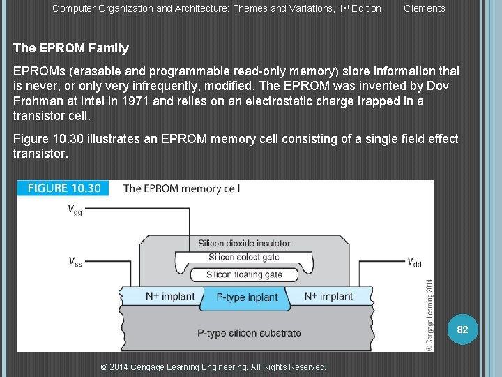
Computer Organization and Architecture: Themes and Variations, 1 st Edition Clements The EPROM Family EPROMs (erasable and programmable read-only memory) store information that is never, or only very infrequently, modified. The EPROM was invented by Dov Frohman at Intel in 1971 and relies on an electrostatic charge trapped in a transistor cell. Figure 10. 30 illustrates an EPROM memory cell consisting of a single field effect transistor. 82 © 2014 Cengage Learning Engineering. All Rights Reserved.

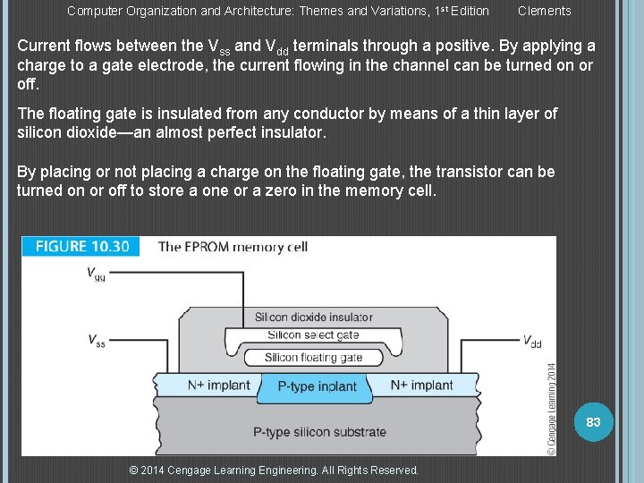
Computer Organization and Architecture: Themes and Variations, 1 st Edition Clements Current flows between the Vss and Vdd terminals through a positive. By applying a charge to a gate electrode, the current flowing in the channel can be turned on or off. The floating gate is insulated from any conductor by means of a thin layer of silicon dioxide—an almost perfect insulator. By placing or not placing a charge on the floating gate, the transistor can be turned on or off to store a one or a zero in the memory cell. 83 © 2014 Cengage Learning Engineering. All Rights Reserved.

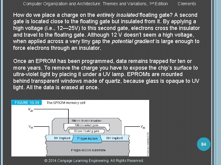
Computer Organization and Architecture: Themes and Variations, 1 st Edition Clements How do we place a charge on the entirely insulated floating gate? A second gate is located close to the floating gate but insulated from it. By applying a high voltage (i. e. , 12— 25 V) to this second gate, electrons cross the insulator and travel to the floating gate. Although 12 V doesn’t seem a high voltage, when applied across a very tiny gap the potential gradient is large enough to force electrons through an insulator. Once an EPROM has been programmed, data remains trapped for ten or more years. To remove the charge you have to expose the chip’s surface to ultra-violet light by placing it under a UV lamp. EPROMs are mounted behind transparent windows made of quartz, because glass is opaque to UV light. All the data is erased at once. 84 © 2014 Cengage Learning Engineering. All Rights Reserved.

Computer Organization and Architecture: Themes and Variations, 1 st Edition Clements First-generation EPROMs had small capacities and were programmed simply by writing the data to each location in turn. Second generation high-capacity EPROMs used smart programming algorithms to apply a short programming pulse to each cell and repeat the operation until the data has been correctly written. Some EPROMs are one-time programmable, OTP, because they lack a quartz window (which is expensive to make) and are programmed once and for all in the field. The EPROM provided a means of developing computer firmware in the laboratory. Unfortunately, its slow programming and its tedious erasure mechanism means that the EPROM is unsuited to consumer applications that require even occasional reprogramming. Today, the UV erasable EPROM is largely obsolete and the few remaining EPROMs are suffering death by e. Bay. © 2014 Cengage Learning Engineering. All Rights Reserved. 85

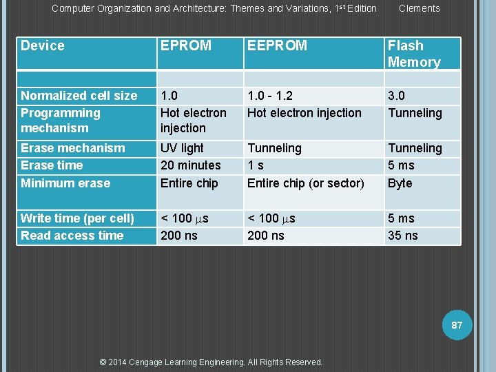
Computer Organization and Architecture: Themes and Variations, 1 st Edition Clements The EEPROM The electrically erasable and reprogrammable EEPROM provides a link between the original EPROM and today’s flash memory. We introduce it to show the development of the EPROM. The major difference between the EEPROM and the flash EEPROM is in the way data is erased. The EEPROM was developed at Intel by George Perlegos in 1978. In an EPROM the trapped electrons in the insulator are removed by the photons of UV light. In an EEPROM the insulating layer is so thin that a quantum mechanical effect, called Fowler-Nordheim tunneling, transports electrons across it when the chip is erased. When a voltage is applied across the insulating layer, electrons on the floating gate are able to tunnel through the layer, even though they don’t have enough energy to cross the barrier. The voltage across the insulating layer is approximately 107 V/cm. Table 10. 3 illustrates the difference between the three programmable devices we describe here. © 2014 Cengage Learning Engineering. All Rights Reserved. 86

Computer Organization and Architecture: Themes and Variations, 1 st Edition Clements Device EPROM EEPROM Flash Memory Normalized cell size Programming mechanism 1. 0 Hot electron injection 1. 0 - 1. 2 Hot electron injection 3. 0 Tunneling Erase mechanism Erase time Minimum erase UV light 20 minutes Entire chip Tunneling 1 s Entire chip (or sector) Tunneling 5 ms Byte Write time (per cell) Read access time < 100 s 200 ns 5 ms 35 ns 87 © 2014 Cengage Learning Engineering. All Rights Reserved.

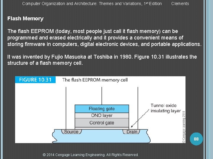
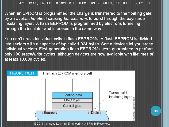
Computer Organization and Architecture: Themes and Variations, 1 st Edition Clements Flash Memory The flash EEPROM (today, most people just call it flash memory) can be programmed and erased electrically and it provides a convenient means of storing firmware in computers, digital electronic devices, and portable applications. It was invented by Fujio Masuoka at Toshiba in 1980. Figure 10. 31 illustrates the structure of a flash memory cell. 88 © 2014 Cengage Learning Engineering. All Rights Reserved.

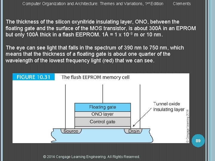
Computer Organization and Architecture: Themes and Variations, 1 st Edition Clements The thickness of the silicon oxynitride insulating layer, ONO, between the floating gate and the surface of the MOS transistor, is about 300Å in an EPROM but only 100Å thick in a flash EEPROM. 1Å = 1 x 10 -9 m or 10 nm. The eye can see light that falls in the spectrum of 390 nm to 750 nm, which means that the thickness of a floating gate is about one quarter of the wavelength of the lowest frequency light (red) that we can see. 89 © 2014 Cengage Learning Engineering. All Rights Reserved.

Computer Organization and Architecture: Themes and Variations, 1 st Edition Clements When an EPROM is programmed, the charge is transferred to the floating gate by an avalanche effect causing hot electrons to burst through the oxynitride insulating layer. A flash EEPROM is programmed by electrons tunneling through the insulator and is erased in the same way. You can’t erase individual cells in flash EEPROMs. A flash EEPROM is divided into sectors with a capacity of typically 1, 024 bytes. Some devices let you erase individual sectors. First-generation flash EEPROMs were guaranteed to perform only 100 erase/write cycles, although devices are now available with lifetimes of at least 10, 000 cycles. 90 © 2014 Cengage Learning Engineering. All Rights Reserved.

Computer Organization and Architecture: Themes and Variations, 1 st Edition Clements Flash EEPROMs are programmed in the same way as the EPROMs. Their read interface to the system is like that of a static RAM, and they have a conventional active-low write-enable input. A write cycle is rather like a conventional write to a static RAM except that the duration of the write is very much longer. A flash EEPROM has an on-chip timer and associated control circuits that automatically ensure the appropriate signal delays without the use of external hardware. Some flash EEPROMs can be programmed a byte at a time, whereas others require an entire sector (e. g. , 1, 024 bytes) to be written in one operation. The erase interface of flash EEPROMs varies from manufacturer to manufacturer. They can be erased in one operation or erased a sector at a time 91 © 2014 Cengage Learning Engineering. All Rights Reserved.

Computer Organization and Architecture: Themes and Variations, 1 st Edition Clements Flash Technology The two pillars of ubiquitous computing are the USB bus and flash memory. The USB bus allows us to connect a wide range of digital systems together (digital camera to PC, or cell phone to i. Pad, and so on) with an absolute minimum of fuss. Data transfer rate and information exchange protocols are handled automatically and invisibly to the user. Similarly, flash memories have grown from 8 MB devices to flash cards that can hold 512 GB in 2010. Interestingly, you can buy a 256 GB flash drive that combines both USB and flash technology to give you a portable storage system capable of holding 256 GB in the palm of your hand (a lifetime’s text and program storage – only images and multimedia require a lot more storage). The continued progress in flash technology saw the introduction of solidstate disk drives in lap top computers in 2010. Replacing hard disks in laptops and note books with flash technology increases performance (data transfer and access time), power consumption, and reliability (there are no vulnerable moving parts). © 2014 Cengage Learning Engineering. All Rights Reserved. 92

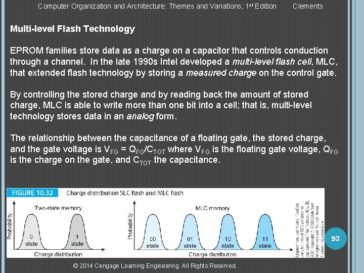
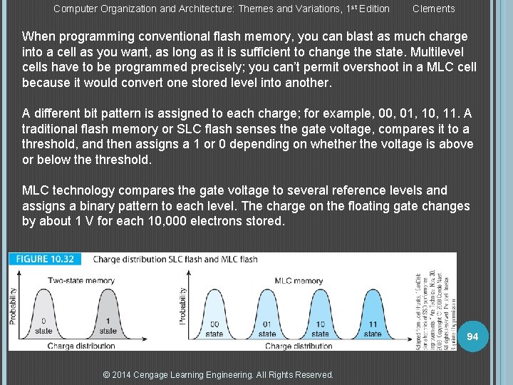
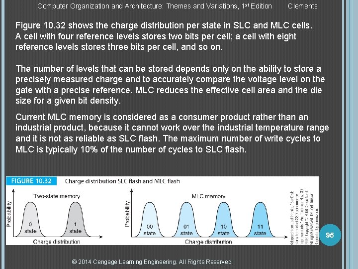
Computer Organization and Architecture: Themes and Variations, 1 st Edition Clements Multi-level Flash Technology EPROM families store data as a charge on a capacitor that controls conduction through a channel. In the late 1990 s Intel developed a multi-level flash cell, MLC, that extended flash technology by storing a measured charge on the control gate. By controlling the stored charge and by reading back the amount of stored charge, MLC is able to write more than one bit into a cell; that is, multi-level technology stores data in an analog form. The relationship between the capacitance of a floating gate, the stored charge, and the gate voltage is VFG = QFG/CTOT where VFG is the floating gate voltage, QFG is the charge on the gate, and CTOT the capacitance. 93 © 2014 Cengage Learning Engineering. All Rights Reserved.

Computer Organization and Architecture: Themes and Variations, 1 st Edition Clements When programming conventional flash memory, you can blast as much charge into a cell as you want, as long as it is sufficient to change the state. Multilevel cells have to be programmed precisely; you can’t permit overshoot in a MLC cell because it would convert one stored level into another. A different bit pattern is assigned to each charge; for example, 00, 01, 10, 11. A traditional flash memory or SLC flash senses the gate voltage, compares it to a threshold, and then assigns a 1 or 0 depending on whether the voltage is above or below the threshold. MLC technology compares the gate voltage to several reference levels and assigns a binary pattern to each level. The charge on the floating gate changes by about 1 V for each 10, 000 electrons stored. 94 © 2014 Cengage Learning Engineering. All Rights Reserved.

Computer Organization and Architecture: Themes and Variations, 1 st Edition Clements Figure 10. 32 shows the charge distribution per state in SLC and MLC cells. A cell with four reference levels stores two bits per cell; a cell with eight reference levels stores three bits per cell, and so on. The number of levels that can be stored depends only on the ability to store a precisely measured charge and to accurately compare the voltage level on the gate with a precise reference. MLC reduces the effective cell area and the die size for a given bit density. Current MLC memory is considered as a consumer product rather than an industrial product, because it cannot work over the industrial temperature range and it is not as reliable as SLC flash. The maximum number of write cycles to MLC is typically 10% of the number of cycles to SLC flash. 95 © 2014 Cengage Learning Engineering. All Rights Reserved.

Computer Organization and Architecture: Themes and Variations, 1 st Edition Clements Aging Transistors Mechanical devices with moving parts such as motors or moving heads (in disks) wear out over time. Conventional wisdom states that devices like transistors never wear out or degrade. This is not true. In early 2011 many were surprised to learn of a defect in a support chip designed for the second-generation Core i 5 and Core i 7 processors. The problem affected the 3 Gbps SATA disk interfaces after a period of operation (estimated as three years). The fault was traced to a transistor that had a too high voltage causing it to degrade over time. This was a stark reminder degrade for several reasons. Over time electrons drift out of the conduction channel to get trapped in the dielectric insulator layer and affect the switching threshold. The dielectric layer can breakdown over time due to electrical stress. Even atoms of the copper or aluminum used to connect the chip gradually diffuse into the silicon and modify its properties. Flash memory is more prone to failure because of the large electrostatic field required to force electrons onto and off the control gate. © 2014 Cengage Learning Engineering. All Rights Reserved. 96

Computer Organization and Architecture: Themes and Variations, 1 st Edition Clements NAND and NOR Flash Modern flash memories are described as being NOR flash or NAND flash. NOR flash was introduced by Intel in 1988 and NAND flash by Toshiba in 1989. The distinction between these two varieties of flash memory lies in the arrangement (i. e. , interconnection) of cells. In general, when people speak of flash memory, they are usually referring to NOR flash. 97 © 2014 Cengage Learning Engineering. All Rights Reserved.

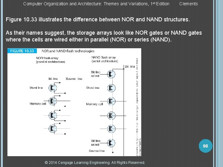
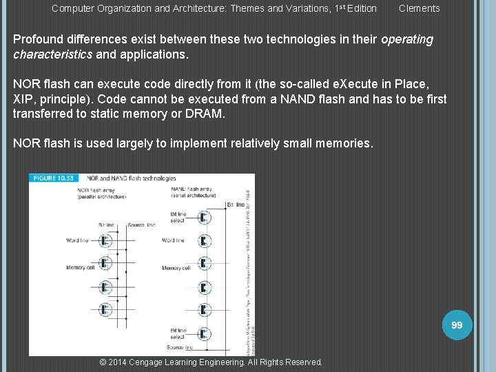
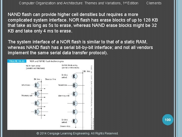
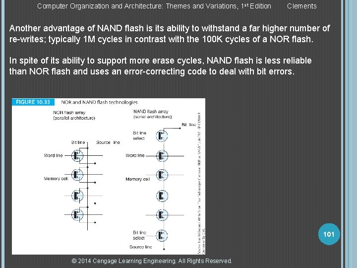
Computer Organization and Architecture: Themes and Variations, 1 st Edition Clements Figure 10. 33 illustrates the difference between NOR and NAND structures. As their names suggest, the storage arrays look like NOR gates or NAND gates where the cells are wired either in parallel (NOR) or series (NAND). 98 © 2014 Cengage Learning Engineering. All Rights Reserved.

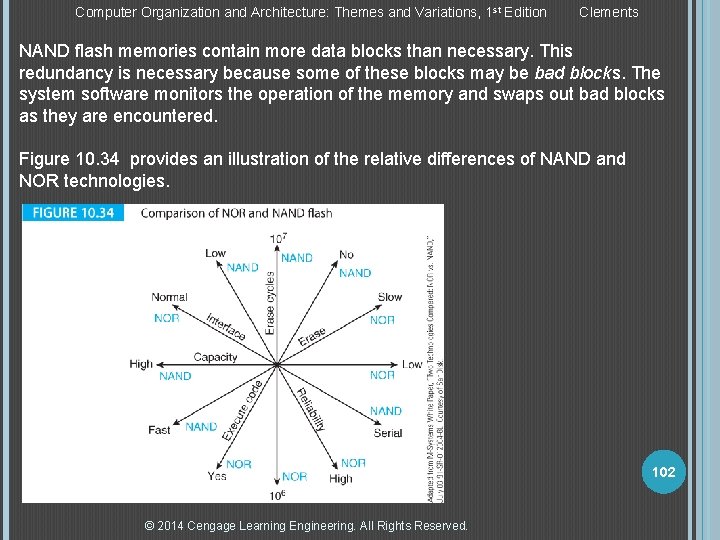
Computer Organization and Architecture: Themes and Variations, 1 st Edition Clements Profound differences exist between these two technologies in their operating characteristics and applications. NOR flash can execute code directly from it (the so-called e. Xecute in Place, XIP, principle). Code cannot be executed from a NAND flash and has to be first transferred to static memory or DRAM. NOR flash is used largely to implement relatively small memories. 99 © 2014 Cengage Learning Engineering. All Rights Reserved.

Computer Organization and Architecture: Themes and Variations, 1 st Edition Clements NAND flash can provide higher cell densities but requires a more complicated system interface. NOR flash has erase blocks of up to 128 KB that take as long as 5 s to erase, whereas NAND erase blocks might be 32 KB and take only 4 ms to erase. The system interface of a NOR flash is similar to that of a static RAM, whereas NAND flash has a serial bit-by-bit interface; and not all vendors implement the same serial data transfer protocol). 100 © 2014 Cengage Learning Engineering. All Rights Reserved.

Computer Organization and Architecture: Themes and Variations, 1 st Edition Clements Another advantage of NAND flash is its ability to withstand a far higher number of re-writes; typically 1 M cycles in contrast with the 100 K cycles of a NOR flash. In spite of its ability to support more erase cycles, NAND flash is less reliable than NOR flash and uses an error-correcting code to deal with bit errors. 101 © 2014 Cengage Learning Engineering. All Rights Reserved.

Computer Organization and Architecture: Themes and Variations, 1 st Edition Clements NAND flash memories contain more data blocks than necessary. This redundancy is necessary because some of these blocks may be bad blocks. The system software monitors the operation of the memory and swaps out bad blocks as they are encountered. Figure 10. 34 provides an illustration of the relative differences of NAND and NOR technologies. 102 © 2014 Cengage Learning Engineering. All Rights Reserved.

Computer Organization and Architecture: Themes and Variations, 1 st Edition Clements Wear Leveling in Flash Memories Flash memory cells have a finite life because of the wear and tear on the insulating layer that takes place when electrons are injected into it or removed from it. If all cells in a flash memory array were accessed and erased equally, all parts of the array would age at the same rate. By its very nature memory is not accessed uniformly; for example, in an MP 3 player some music may remain unheard and other tracks frequently played. Consequently, some cells in an array may wear out prematurely while other cells are still capable of many more erase cycles. Flash wear leveling mitigates against the uneven distribution of erase cycles. Static wear leveling moves fixed data to higher-use regions of the flash memory and allocates the less frequently used areas to frequently-changing data; that is, an attempt is made to balance the number of accesses to the array. More sophisticated dynamic leveling algorithms exist to monitor the use of the flash array and then to swap out high-use blocks of data with low-use blocks of data when the need arises. © 2014 Cengage Learning Engineering. All Rights Reserved. 103

Computer Organization and Architecture: Themes and Variations, 1 st Edition Clements New and Emerging Non-volatile Technologies We first look at two mature emerging technologies ferroelectric RAM and Ovonic memory. FRAM or ferroelectric RAM, a form of semiconductor random access nonvolatile memory, began to emerge during the late 1990 s. DRAM stores an electric charge by displacing the electrons in a material. Disk and tape systems store a magnetic field by aligning the spin of adjacent electrons in the recording medium. FRAM stores data by changing the polarization in a material by moving individual atoms within a crystal lattice. 104 © 2014 Cengage Learning Engineering. All Rights Reserved.

Computer Organization and Architecture: Themes and Variations, 1 st Edition Clements The ferroelectric effect describes the ability of a material to store an electric polarization in the absence of an applied magnetic field. Materials can be divided into two classes; conductors and insulators. The difference between these is that electrons are free to move through a conductor, but are not free to move in an insulator. If you apply an electric field to a conductor such as copper, the electrons in the conductor move under the influence of the field. If an insulator is placed in an electric field, the electrons are not free to move through the insulator. However, the electric field does have an effect on the molecules that make up the insulator; it disturbs the symmetrical distribution of positive and negative charges in the molecular structure of the insulator. This change in the position of electrons and nuclei under the influence of an electric field is called polarization. 105 © 2014 Cengage Learning Engineering. All Rights Reserved.

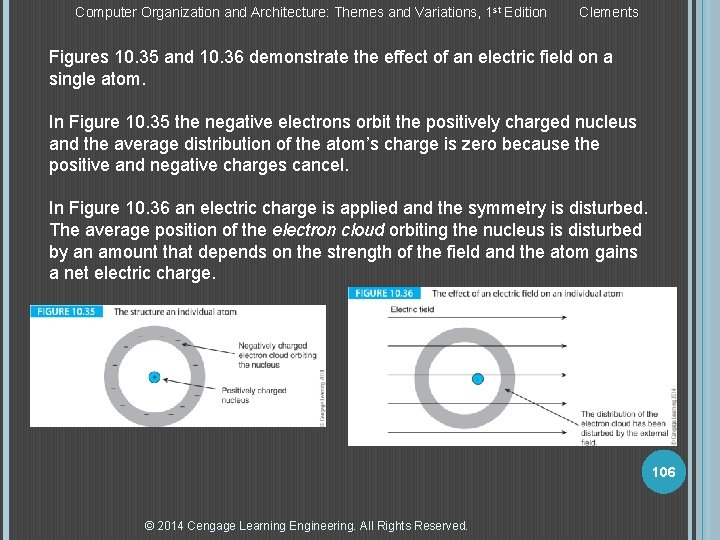
Computer Organization and Architecture: Themes and Variations, 1 st Edition Clements Figures 10. 35 and 10. 36 demonstrate the effect of an electric field on a single atom. In Figure 10. 35 the negative electrons orbit the positively charged nucleus and the average distribution of the atom’s charge is zero because the positive and negative charges cancel. In Figure 10. 36 an electric charge is applied and the symmetry is disturbed. The average position of the electron cloud orbiting the nucleus is disturbed by an amount that depends on the strength of the field and the atom gains a net electric charge. 106 © 2014 Cengage Learning Engineering. All Rights Reserved.

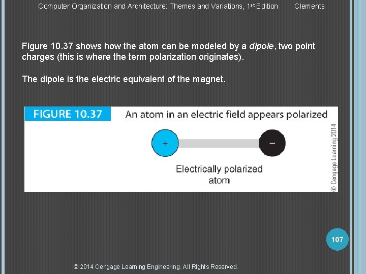
Computer Organization and Architecture: Themes and Variations, 1 st Edition Clements Figure 10. 37 shows how the atom can be modeled by a dipole, two point charges (this is where the term polarization originates). The dipole is the electric equivalent of the magnet. 107 © 2014 Cengage Learning Engineering. All Rights Reserved.

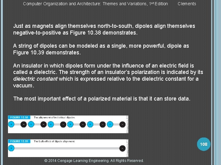
Computer Organization and Architecture: Themes and Variations, 1 st Edition Clements Just as magnets align themselves north-to-south, dipoles align themselves negative-to-positive as Figure 10. 38 demonstrates. A string of dipoles can be modeled as a single, more powerful, dipole as Figure 10. 39 demonstrates. An insulator in which dipoles form under the influence of an electric field is called a dielectric. The strength of an insulator’s polarization is indicated by its dielectric constant which is expressed relative to the dielectric constant for a vacuum. The most important effect of a polarized material is that it can store data. 108 © 2014 Cengage Learning Engineering. All Rights Reserved.

Computer Organization and Architecture: Themes and Variations, 1 st Edition Clements FRAM is a practical application of the ferroelectric effect. A thin ferroelectric film is used as the dielectric in a tiny capacitor to store data. Ferroelectric films electrically polarize in one of two directions, depending on the direction in which the electric field is applied. The use of ferroelectric technology was investigated at Stanford University in the early 1960 s and S. Y. Wu et al investigated the use of ferroelectric materials in conjunction with semiconductor technology in 1974. In 1988, Ramtron International Corporation announced the first commercial Ferroelectric Random Access Memory (FRAM). The ferroelectric materials used in FRAM memories belong to the class of crystals called perovskite. 109 © 2014 Cengage Learning Engineering. All Rights Reserved.

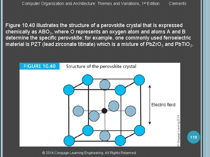
Computer Organization and Architecture: Themes and Variations, 1 st Edition Clements Figure 10. 40 illustrates the structure of a perovskite crystal that is expressed chemically as ABO 3, where O represents an oxygen atom and atoms A and B determine the specific perovskite; for example, one commonly used ferroelectric material is PZT (lead zirconate titinate) which is a mixture of Pb. Zr. O 3 and Pb. Ti. O 3. 110 © 2014 Cengage Learning Engineering. All Rights Reserved.

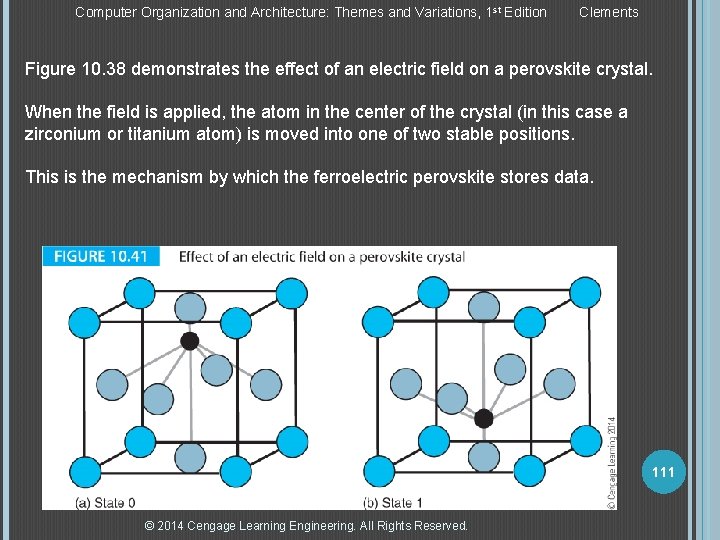
Computer Organization and Architecture: Themes and Variations, 1 st Edition Clements Figure 10. 38 demonstrates the effect of an electric field on a perovskite crystal. When the field is applied, the atom in the center of the crystal (in this case a zirconium or titanium atom) is moved into one of two stable positions. This is the mechanism by which the ferroelectric perovskite stores data. 111 © 2014 Cengage Learning Engineering. All Rights Reserved.

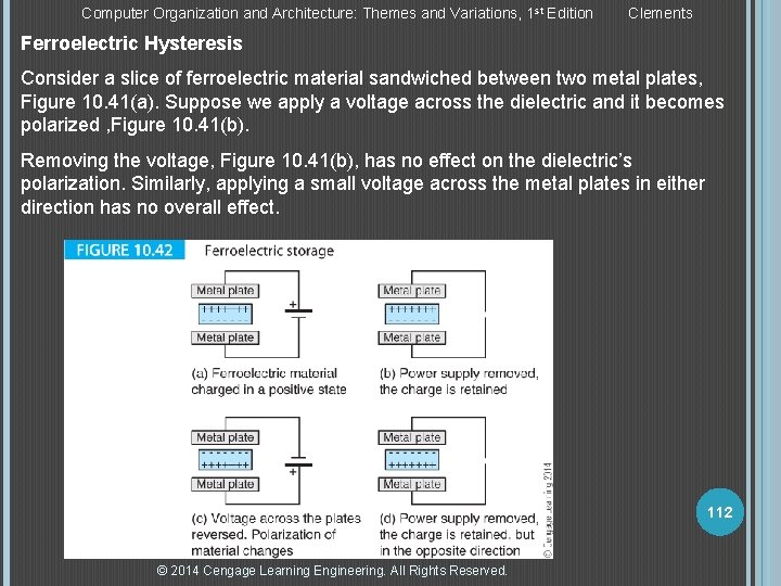
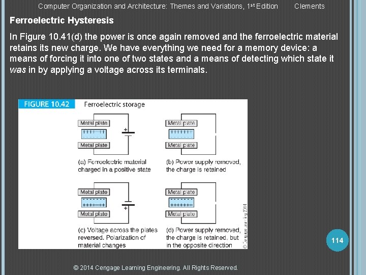
Computer Organization and Architecture: Themes and Variations, 1 st Edition Clements Ferroelectric Hysteresis Consider a slice of ferroelectric material sandwiched between two metal plates, Figure 10. 41(a). Suppose we apply a voltage across the dielectric and it becomes polarized , Figure 10. 41(b). Removing the voltage, Figure 10. 41(b), has no effect on the dielectric’s polarization. Similarly, applying a small voltage across the metal plates in either direction has no overall effect. 112 © 2014 Cengage Learning Engineering. All Rights Reserved.

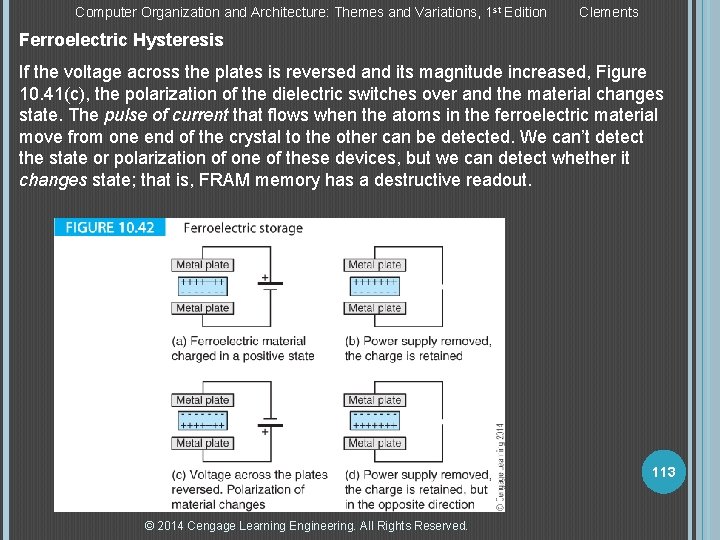
Computer Organization and Architecture: Themes and Variations, 1 st Edition Clements Ferroelectric Hysteresis If the voltage across the plates is reversed and its magnitude increased, Figure 10. 41(c), the polarization of the dielectric switches over and the material changes state. The pulse of current that flows when the atoms in the ferroelectric material move from one end of the crystal to the other can be detected. We can’t detect the state or polarization of one of these devices, but we can detect whether it changes state; that is, FRAM memory has a destructive readout. 113 © 2014 Cengage Learning Engineering. All Rights Reserved.

Computer Organization and Architecture: Themes and Variations, 1 st Edition Clements Ferroelectric Hysteresis In Figure 10. 41(d) the power is once again removed and the ferroelectric material retains its new charge. We have everything we need for a memory device: a means of forcing it into one of two states and a means of detecting which state it was in by applying a voltage across its terminals. 114 © 2014 Cengage Learning Engineering. All Rights Reserved.

Computer Organization and Architecture: Themes and Variations, 1 st Edition Clements A practical FRAM memory cell is constructed using slightly modified DRAM technology. We have just seen that writing data into an FRAM cell is achieved by applying a charge across the ferroelectric material. In order to read the data stored in the cell, the transistor is turned on and an electric field applied across the capacitor. If the cell is already polarized in the same direction as the applied field, nothing will happen. If, however, the cell is charged in the reverse direction, a current flows through the switching transistor. 115 © 2014 Cengage Learning Engineering. All Rights Reserved.

Computer Organization and Architecture: Themes and Variations, 1 st Edition Clements The FRAM cell changes state in about 100 ns, which is faster than some conventional semiconductor nonvolatile memories such as EPROM, but slower than either static RAM or DRAM. The act of reading a FRAM cell is, of course, destructive, because data is sensed by the cell changing state or not changing state. Consequently, a FRAM read cycle must always be followed by a write cycle to write back the data that may or may not have changed. 116 © 2014 Cengage Learning Engineering. All Rights Reserved.

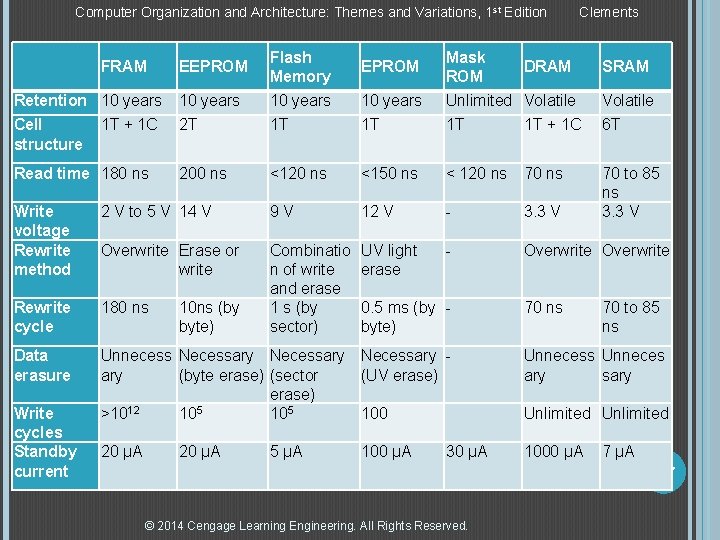
Computer Organization and Architecture: Themes and Variations, 1 st Edition Clements EEPROM Flash Memory EPROM Mask ROM Retention 10 years Unlimited Volatile Cell structure 2 T 1 T 1 T + 1 C 6 T 200 ns <120 ns <150 ns < 120 ns 70 to 85 ns 3. 3 V FRAM 1 T + 1 C Read time 180 ns DRAM SRAM Write voltage Rewrite method 2 V to 5 V 14 V 9 V 12 V - 3. 3 V Overwrite Erase or write UV light erase - Overwrite Rewrite cycle 180 ns Combinatio n of write and erase 1 s (by sector) Data erasure Unnecess Necessary (byte erase) (sector (UV erase) >1012 105 100 Unnecess Unneces ary sary 20 µA 1000 µA Write cycles Standby current 10 ns (by byte) 20 µA 5 µA 0. 5 ms (by byte) 100 µA 30 µA 70 ns 70 to 85 ns Unlimited 7 µA 117 © 2014 Cengage Learning Engineering. All Rights Reserved.

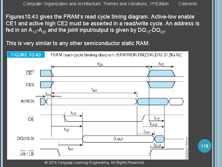
Computer Organization and Architecture: Themes and Variations, 1 st Edition Clements Figures 10. 43 gives the FRAM’s read cycle timing diagram. Active-low enable CE 1 and active high CE 2 must be asserted in a read/write cycle. An address is fed in on A 18 -A 00 and the joint input/output is given by DQ 15 -DQ 00. This is very similar to any other semiconductor static RAM. 118 © 2014 Cengage Learning Engineering. All Rights Reserved.

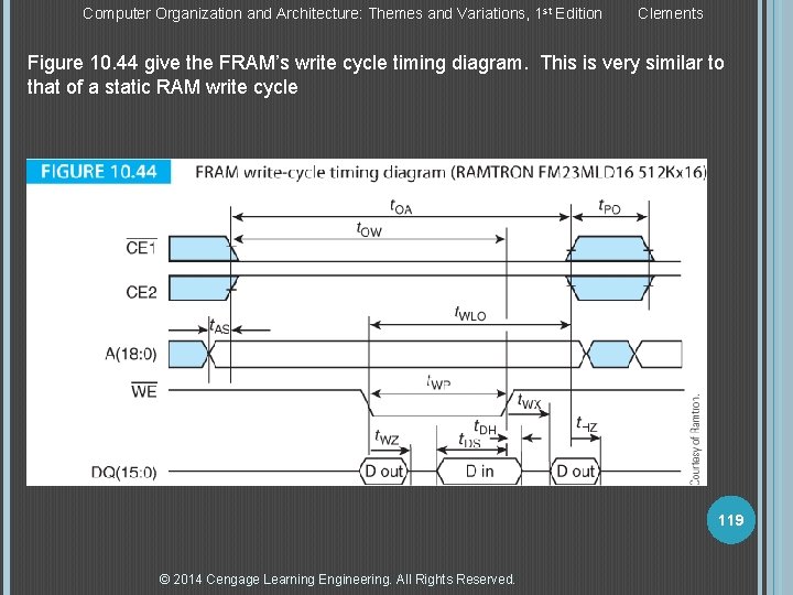
Computer Organization and Architecture: Themes and Variations, 1 st Edition Clements Figure 10. 44 give the FRAM’s write cycle timing diagram. This is very similar to that of a static RAM write cycle 119 © 2014 Cengage Learning Engineering. All Rights Reserved.

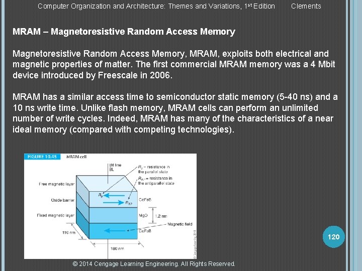
Computer Organization and Architecture: Themes and Variations, 1 st Edition Clements MRAM – Magnetoresistive Random Access Memory, MRAM, exploits both electrical and magnetic properties of matter. The first commercial MRAM memory was a 4 Mbit device introduced by Freescale in 2006. MRAM has a similar access time to semiconductor static memory (5 -40 ns) and a 10 ns write time. Unlike flash memory, MRAM cells can perform an unlimited number of write cycles. Indeed, MRAM has many of the characteristics of a near ideal memory (compared with competing technologies). 120 © 2014 Cengage Learning Engineering. All Rights Reserved.

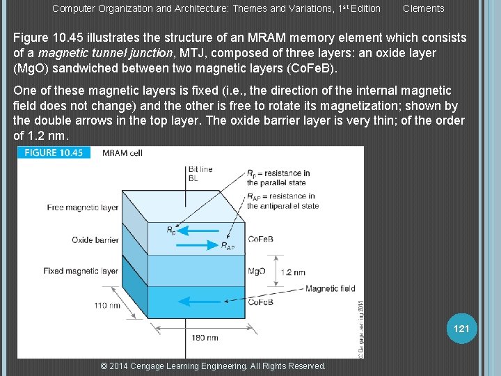
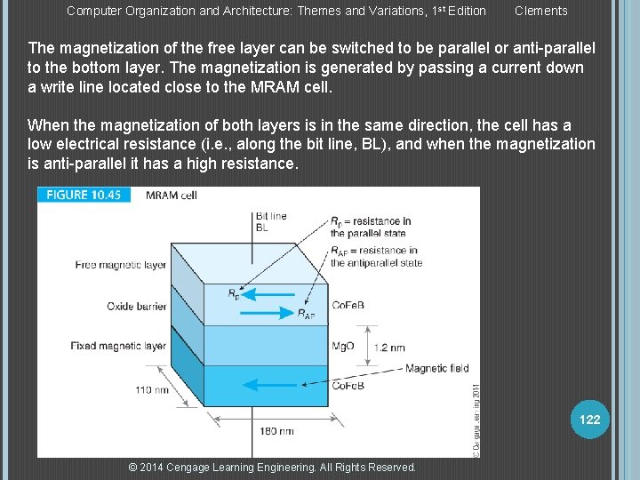
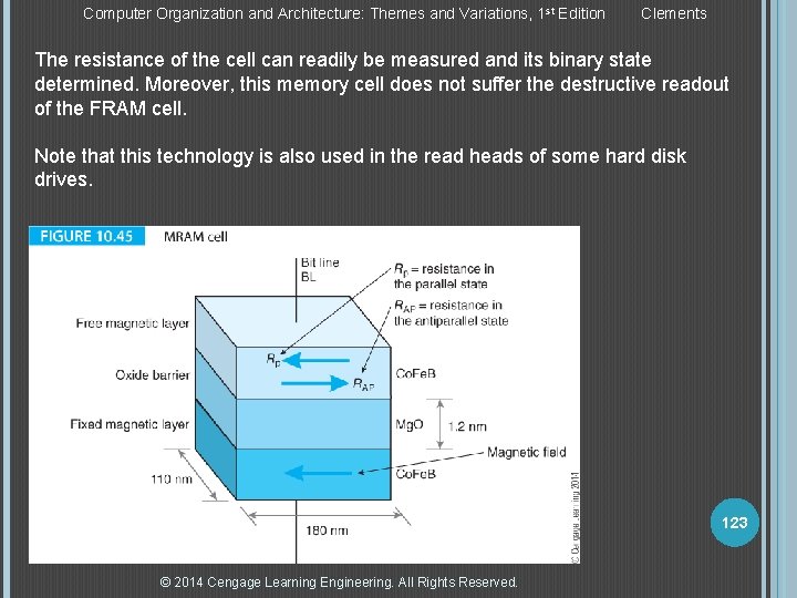
Computer Organization and Architecture: Themes and Variations, 1 st Edition Clements Figure 10. 45 illustrates the structure of an MRAM memory element which consists of a magnetic tunnel junction, MTJ, composed of three layers: an oxide layer (Mg. O) sandwiched between two magnetic layers (Co. Fe. B). One of these magnetic layers is fixed (i. e. , the direction of the internal magnetic field does not change) and the other is free to rotate its magnetization; shown by the double arrows in the top layer. The oxide barrier layer is very thin; of the order of 1. 2 nm. 121 © 2014 Cengage Learning Engineering. All Rights Reserved.

Computer Organization and Architecture: Themes and Variations, 1 st Edition Clements The magnetization of the free layer can be switched to be parallel or anti-parallel to the bottom layer. The magnetization is generated by passing a current down a write line located close to the MRAM cell. When the magnetization of both layers is in the same direction, the cell has a low electrical resistance (i. e. , along the bit line, BL), and when the magnetization is anti-parallel it has a high resistance. 122 © 2014 Cengage Learning Engineering. All Rights Reserved.

Computer Organization and Architecture: Themes and Variations, 1 st Edition Clements The resistance of the cell can readily be measured and its binary state determined. Moreover, this memory cell does not suffer the destructive readout of the FRAM cell. Note that this technology is also used in the read heads of some hard disk drives. 123 © 2014 Cengage Learning Engineering. All Rights Reserved.

Computer Organization and Architecture: Themes and Variations, 1 st Edition Clements Ovonic Memory A property of matter that can be used to store information is its phase, which Ovonic memory to store data. This phase change is reversible so that the cells can be erased and rewritten. An Ovonic material is either in a structured crystalline state or an amorphous noncrystalline state. A class of materials with suitable phase-change properties is the chalcogenide glasses, investigated by Ovshinsky at Bell Labs in 1968. If a chalcogenide glass is melted and cooled rapidly, it enters an amorphous phase. If it is heated to slightly below its melting temperature at a relatively slow rate, the amorphous material reverts to its initial crystalline phase. An amorphous material is characterized by high reflectivity and high electrical resistivity, whereas a polycrystalline material is characterized by low reflectivity and a low electrical resistance. 124 © 2014 Cengage Learning Engineering. All Rights Reserved.

Computer Organization and Architecture: Themes and Variations, 1 st Edition Clements Ovonic Memory An Ovonic cell can be read because there is a forty-fold difference in the electrical resistance of the material in these two states. Because the chalcogenide can be fabricated as a thin film, it can be incorporated in a semiconductor cell and an Ovonic memory constructed just like any other semiconductor memory. Unlike flash memory, phase change memory can be bit-organized in the sense that individual bits can be re-written. Flash memory is block-organized and you have to erase an entire block (sector) in order to make a change. Ovonic memory is static and has no need for a refresh; the data readout is nondestructive. By controlling the amplitude of the current pulse used to write data into a cell, it is possible to select one of several amorphous states each with its own electrical resistance. Consequently, Ovonic memory is a candidate for multi-bit storage cells that will boost the density of bits/chip. 125 © 2014 Cengage Learning Engineering. All Rights Reserved.

Computer Organization and Architecture: Themes and Variations, 1 st Edition Clements Ovonic Memory Ovonic cells are capable of more than 1013 phase changes without degradation. A further advantage of Ovonic memory is its stability. At normal operating temperatures it is estimated that the contents of a memory cell will remain stable for over 300 years. Similarly, the projected lifetime in terms of read/write cycles is greater for a phase-change device than a flash memory cell. Flash memory and DRAM that store data in the form of a charge are susceptible to the effects of ionizing radiation which preclude them for some space and military applications. Phase-change memory devices are intrinsically radiation-hard. 126 © 2014 Cengage Learning Engineering. All Rights Reserved.