The ARM Architecture T H E A R











- Slides: 61
The ARM Architecture T H E A R C H I T E C T U R E F O R T TM H E D I G I T A L W O R 1 L D
Day 9 Agenda n Introduction to ARM Ltd The ARM Architecture Programmers Model Instruction Set 39 v 10 The ARM Architecture TM 2 2
ARM Ltd n Founded in November 1990 n Spun out of Acorn Computers n Designs the ARM range of RISC processor cores n Licenses ARM core designs to semiconductor partners who fabricate and sell to their customers. n n ARM does not fabricate silicon itself Also develop technologies to assist with the design-in of the ARM architecture n Software tools, boards, debug hardware, application software, bus architectures, peripherals etc 39 v 10 The ARM Architecture TM 3 3
Intellectual Property n ARM provides hard and soft views to licensees n n n RTL and synthesis flows GDSII layout (Geometric database standard information interchange) Licencees have the right to use hard or soft views of the IP n soft views include gate level netlists 39 v 10 The ARM Architecture TM 4 4
ARM Partnership Model 39 v 10 The ARM Architecture TM 5 5
ARM Powered Products 39 v 10 The ARM Architecture TM 6 6
Agenda Introduction n The ARM Architecture Overview Programmers Model Instruction Set 39 v 10 The ARM Architecture TM 7 7
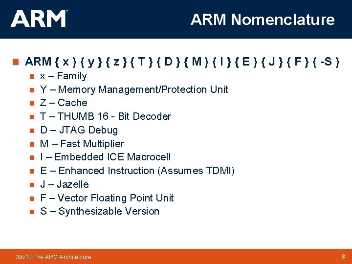
ARM Nomenclature n ARM { x } { y } { z } { T } { D } { M } { I } { E } { J } { F } { -S } n n n x – Family Y – Memory Management/Protection Unit Z – Cache T – THUMB 16 - Bit Decoder D – JTAG Debug M – Fast Multiplier I – Embedded ICE Macrocell E – Enhanced Instruction (Assumes TDMI) J – Jazelle F – Vector Floating Point Unit S – Synthesizable Version 39 v 10 The ARM Architecture TM 8 8
The ARM Architecture Evolution n Architecture n Versions 1 and 2 -- Acorn RISC, 26 -bit address n Version 3 – 32 -bit address, CPSR, and SPSR n Version 4 – half-word, Thumb n Version 5 n Processor cores n ARM 7 TDMI (Thumb, debug, multiplier, ICE) – version 4 T, low end n ARM core, 3 -stage pipeline n ARM 9 TDMI – 5 -stage pipeline n ARM 10 TDMI – version 5 n CPU Core: co-processor, MMU, AMBA n ARM 710, 720, 740 n ARM 920, 940 39 v 10 The ARM Architecture TM 9 9
The Core 39 v 10 The ARM Architecture TM 10 10
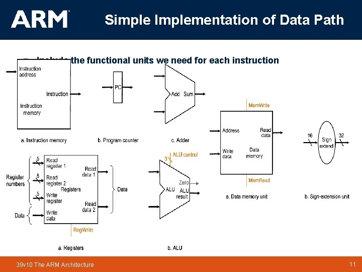
Simple Implementation of Data Path n Include the functional units we need for each instruction 39 v 10 The ARM Architecture TM 11 11
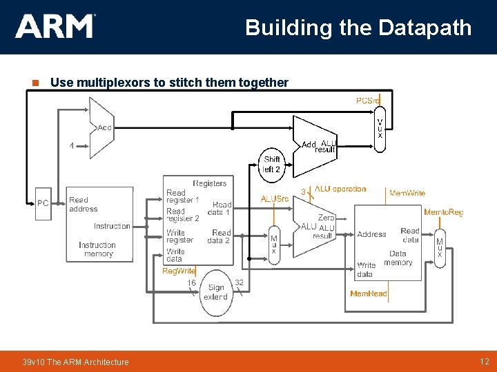
Building the Datapath n Use multiplexors to stitch them together 39 v 10 The ARM Architecture TM 12 12
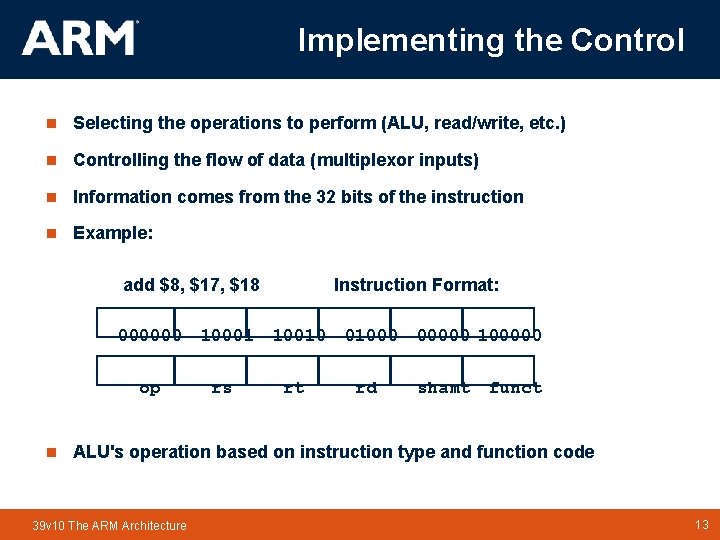
Implementing the Control n Selecting the operations to perform (ALU, read/write, etc. ) n Controlling the flow of data (multiplexor inputs) n Information comes from the 32 bits of the instruction n Example: add $8, $17, $18 000000 op n Instruction Format: 10001 10010 01000 00000 100000 rs rt rd shamt funct ALU's operation based on instruction type and function code 39 v 10 The ARM Architecture TM 13 13
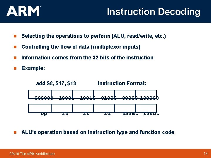
Instruction Decoding n Selecting the operations to perform (ALU, read/write, etc. ) n Controlling the flow of data (multiplexor inputs) n Information comes from the 32 bits of the instruction n Example: add $8, $17, $18 000000 op n Instruction Format: 10001 10010 01000 00000 100000 rs rt rd shamt funct ALU's operation based on instruction type and function code 39 v 10 The ARM Architecture TM 14 14
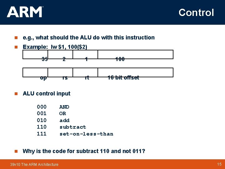
Control n e. g. , what should the ALU do with this instruction n Example: lw $1, 100($2) n 35 2 1 op rs rt 16 bit offset ALU control input 000 001 010 111 n 100 AND OR add subtract set-on-less-than Why is the code for subtract 110 and not 011? 39 v 10 The ARM Architecture TM 15 15
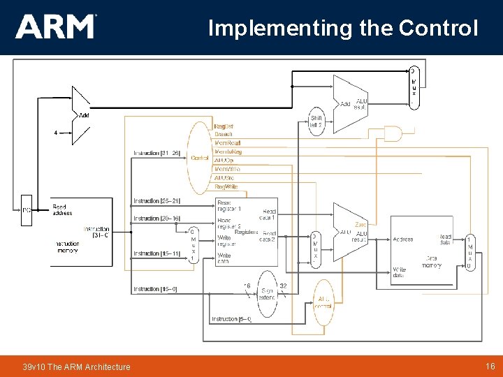
Implementing the Control 39 v 10 The ARM Architecture TM 16 16
The Core 39 v 10 The ARM Architecture TM 17 17
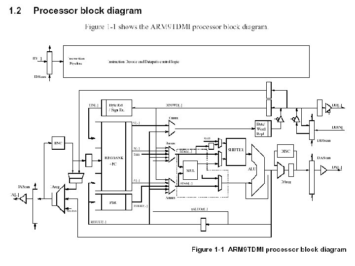
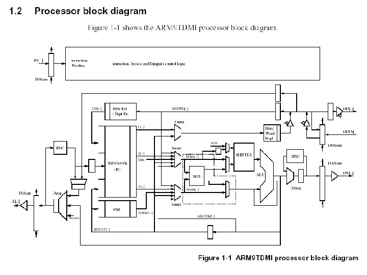
ARM 9 TDMI Core Features n Based on Harvard Architecture n 32 Bit ARM Instruction set n 16 Bit Thumb Instruction set n 37 General Purpose Registers n Supports Hardware and Software Debug n Bi and Uni-directional connection to external Memory Systems n Supports Co-Processor n It uses 5 stage pipelining n Fetch, Decode, Execute, Memory and Write 39 v 10 The ARM Architecture TM 18 18
Agenda Introduction The ARM Architecture Overview n Programmers Model Instruction Set 39 v 10 The ARM Architecture TM 19 19
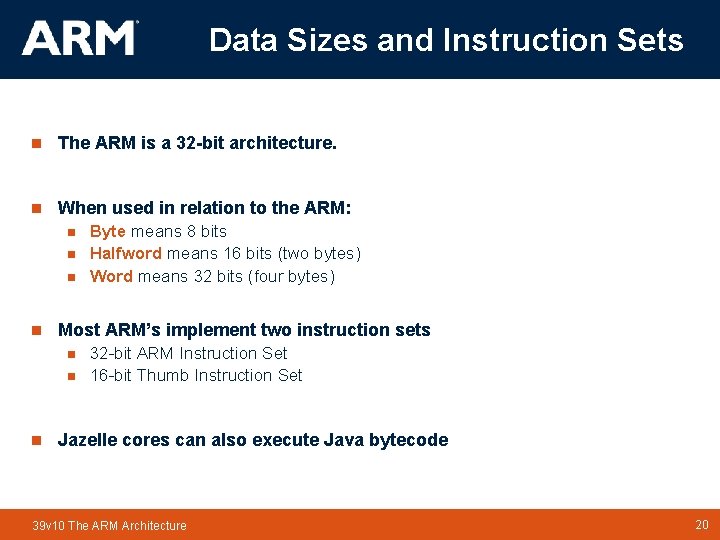
Data Sizes and Instruction Sets n The ARM is a 32 -bit architecture. n When used in relation to the ARM: n n Most ARM’s implement two instruction sets n n n Byte means 8 bits Halfword means 16 bits (two bytes) Word means 32 bits (four bytes) 32 -bit ARM Instruction Set 16 -bit Thumb Instruction Set Jazelle cores can also execute Java bytecode 39 v 10 The ARM Architecture TM 20 20
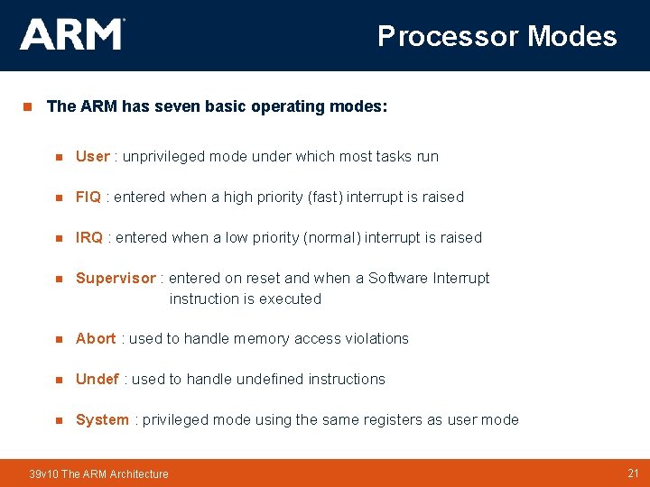
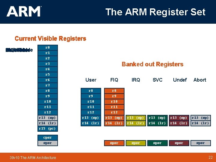
Processor Modes n The ARM has seven basic operating modes: n User : unprivileged mode under which most tasks run n FIQ : entered when a high priority (fast) interrupt is raised n IRQ : entered when a low priority (normal) interrupt is raised n Supervisor : entered on reset and when a Software Interrupt instruction is executed n Abort : used to handle memory access violations n Undef : used to handle undefined instructions n System : privileged mode using the same registers as user mode 39 v 10 The ARM Architecture TM 21 21
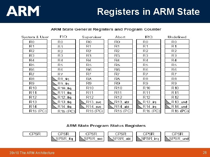
The ARM Register Set Current Visible Registers Abort Mode Undef SVC Mode FIQ User Mode IRQ Mode r 0 r 1 r 2 r 3 r 4 r 5 r 6 r 7 r 8 r 9 r 10 r 11 r 12 r 13 (sp) r 14 (lr) r 15 (pc) cpsr spsr 39 v 10 The ARM Architecture Banked out Registers User FIQ IRQ SVC Undef Abort r 8 r 9 r 10 r 11 r 12 r 13 (sp) r 14 (lr) r 13 (sp) r 14 (lr) spsr spsr TM 22 22
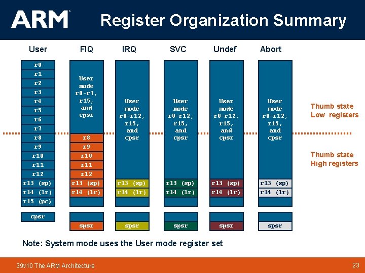
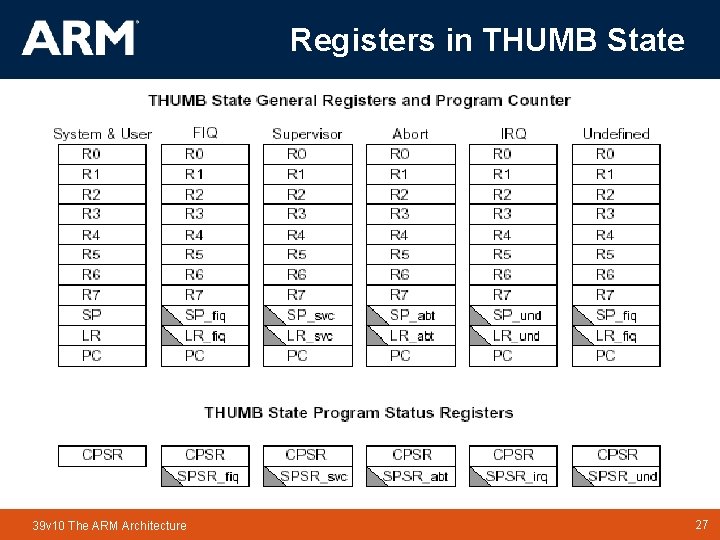
Register Organization Summary User FIQ IRQ SVC Undef User mode r 0 -r 12, r 15, and cpsr Abort r 0 r 1 r 2 r 3 r 4 r 5 r 6 r 7 r 8 r 9 r 10 r 11 r 12 r 13 (sp) r 14 (lr) r 15 (pc) User mode r 0 -r 7, r 15, and cpsr User mode r 0 -r 12, r 15, and cpsr r 8 r 9 r 10 r 11 r 12 r 13 (sp) r 14 (lr) r 13 (sp) r 14 (lr) spsr spsr Thumb state Low registers Thumb state High registers cpsr Note: System mode uses the User mode register set 39 v 10 The ARM Architecture TM 23 23
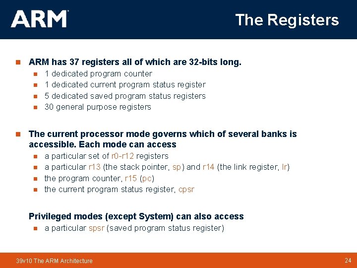
The Registers n ARM has 37 registers all of which are 32 -bits long. n n n 1 dedicated program counter 1 dedicated current program status register 5 dedicated saved program status registers 30 general purpose registers The current processor mode governs which of several banks is accessible. Each mode can access n n a particular set of r 0 -r 12 registers a particular r 13 (the stack pointer, sp) and r 14 (the link register, lr) the program counter, r 15 (pc) the current program status register, cpsr Privileged modes (except System) can also access n a particular spsr (saved program status register) 39 v 10 The ARM Architecture TM 24 24
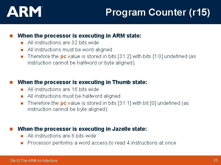
Program Counter (r 15) n When the processor is executing in ARM state: n n When the processor is executing in Thumb state: n n All instructions are 32 bits wide All instructions must be word aligned Therefore the pc value is stored in bits [31: 2] with bits [1: 0] undefined (as instruction cannot be halfword or byte aligned). All instructions are 16 bits wide All instructions must be halfword aligned Therefore the pc value is stored in bits [31: 1] with bit [0] undefined (as instruction cannot be byte aligned). When the processor is executing in Jazelle state: n n All instructions are 8 bits wide Processor performs a word access to read 4 instructions at once 39 v 10 The ARM Architecture TM 25 25
Registers in ARM State 39 v 10 The ARM Architecture TM 26 26
Registers in THUMB State 39 v 10 The ARM Architecture TM 27 27
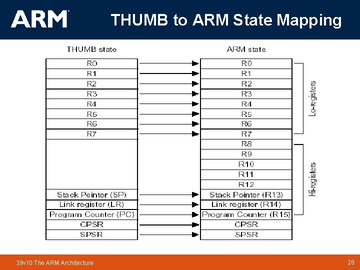
THUMB to ARM State Mapping 39 v 10 The ARM Architecture TM 28 28
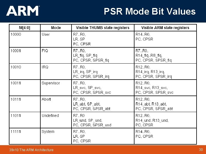
Current Program Status Registers 31 28 27 N Z C V Q 24 J 23 16 15 U f n n d e f n n e s Condition code flags n i 8 N = Negative result from ALU Z = Zero result from ALU C = ALU operation Carried out V = ALU operation o. Verflowed x n n n Architecture 5 TE/J only Indicates if saturation has occurred n J bit n n 4 0 I F T mode c I = 1: Disables the IRQ. F = 1: Disables the FIQ. Architecture x. T only T = 0: Processor in ARM state T = 1: Processor in Thumb state Mode bits n n 5 T Bit n Sticky Overflow flag - Q flag n 6 Interrupt Disable bits. n n n d 7 Specify the processor mode Architecture 5 TEJ only J = 1: Processor in Jazelle state 39 v 10 The ARM Architecture TM 29 29
PSR Mode Bit Values 39 v 10 The ARM Architecture TM 30 30
Agenda Introduction The ARM Architecture Overview Programmers Model n Instruction Set 39 v 10 The ARM Architecture TM 31 31
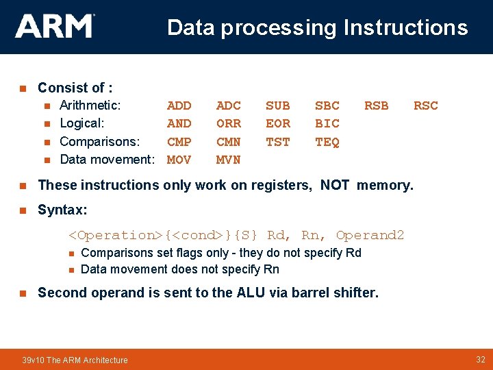
Data processing Instructions n Consist of : n n Arithmetic: Logical: Comparisons: Data movement: ADD AND CMP MOV ADC ORR CMN MVN SUB EOR TST SBC BIC TEQ RSB RSC n These instructions only work on registers, NOT memory. n Syntax: <Operation>{<cond>}{S} Rd, Rn, Operand 2 n n n Comparisons set flags only - they do not specify Rd Data movement does not specify Rn Second operand is sent to the ALU via barrel shifter. 39 v 10 The ARM Architecture TM 32 32
Instruction Encoding [15: 12] Destination register [19: 16] 1 st operand register [16] 0: Branch 1: Branch and Link [20] Set condition codes 0 = Do not set condition codes 1 = Set condition codes [24: 21] Operation codes 0000 = AND-Rd: = Op 1 AND Op 2 0001 = EOR-Rd: = Op 1 EOR Op 2 0010 = SUB-Rd: = Op 1 -Op 2 0011 = RSB-Rd: = Op 2 -Op 1 0100 = ADD-Rd: = Op 1+Op 2 0101 = ADC-Rd: = Op 1+Op 2+C 0110 = SBC-Rd: = OP 1 -Op 2+C-1 0111 = RSC-Rd: = Op 2 -Op 1+C-1 39 v 10 The ARM Architecture Assemble as AND Rd, Ra, Rb EOR Rd, Ra, Rb SUB Rd, Ra, Rb RSB Rd, Ra, Rb ADD Rd, Ra, Rb ADC Rd, Ra, Rb SBC Rd, Ra, Rb RSC Rd, Ra, Rb TM 33 33
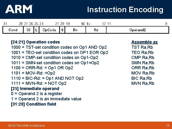
Instruction Encoding [24: 21] Operation codes 1000 = TST-set condition codes on Op 1 AND Op 2 1001 = TEO-set condition codes on OP 1 EOR Op 2 1010 = CMP-set condition codes on Op 1 -Op 2 1011 = SMN-set condition codes on Op 1+Op 2 1100 = ORR-Rd: = Op 1 OR Op 2 1101 = MOV-Rd: =Op 2 1110 = BIC-Rd: = Op 1 AND NOT Op 2 1111 = MVN-Rd: = NOT Op 2 [25] Immediate operand 0 = Operand 2 is a register 1 = Operand 2 is an immediate value [31: 28] Condition field 39 v 10 The ARM Architecture TM Assemble as TST Ra, Rb TEO Ra, Rb CMP Ra, Rb SMN Ra, Rb ORR Ra, Rb MOV Ra, Rb BIC Ra, Rb MVN Ra, Rb 34 34
Condition Codes n n Suffix Description Flags tested EQ Equal Z=1 The possible condition codes are listed: NE Not equal Z=0 CS/HS Unsigned higher or same C=1 CC/LO Unsigned lower C=0 MI Minus N=1 PL Positive or Zero N=0 Note AL is the default and does not need to be specified VS Overflow V=1 VC No overflow V=0 HI Unsigned higher C=1 & Z=0 LS Unsigned lower or same C=0 or Z=1 GE Greater or equal N=V LT Less than N!=V GT Greater than Z=0 & N=V LE Less than or equal Z=1 or N=!V AL Always 39 v 10 The ARM Architecture TM 35 35
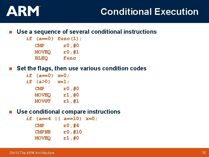
Conditional Execution n Use a sequence of several conditional instructions if (a==0) func(1); CMP r 0, #0 MOVEQ r 0, #1 BLEQ func n Set the flags, then use various condition codes if (a==0) x=0; if (a>0) x=1; CMP r 0, #0 MOVEQ r 1, #0 MOVGT r 1, #1 n Use conditional compare instructions if (a==4 || a==10) x=0; CMP r 0, #4 CMPNE r 0, #10 MOVEQ r 1, #0 39 v 10 The ARM Architecture TM 36 36
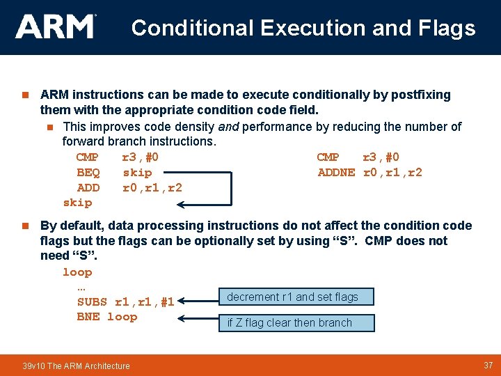
Conditional Execution and Flags n ARM instructions can be made to execute conditionally by postfixing them with the appropriate condition code field. n This improves code density and performance by reducing the number of forward branch instructions. CMP r 3, #0 BEQ skip ADDNE r 0, r 1, r 2 ADD r 0, r 1, r 2 skip n By default, data processing instructions do not affect the condition code flags but the flags can be optionally set by using “S”. CMP does not need “S”. loop … decrement r 1 and set flags SUBS r 1, #1 BNE loop if Z flag clear then branch 39 v 10 The ARM Architecture TM 37 37
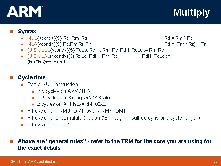
Multiply n Syntax: n n n MUL{<cond>}{S} Rd, Rm, Rs Rd = Rm * Rs MLA{<cond>}{S} Rd, Rm, Rs, Rn Rd = (Rm * Rs) + Rn [U|S]MULL{<cond>}{S} Rd. Lo, Rd. Hi, Rm, Rs Rd. Hi, Rd. Lo : = Rm*Rs [U|S]MLAL{<cond>}{S} Rd. Lo, Rd. Hi, Rm, Rs Rd. Hi, Rd. Lo : = (Rm*Rs)+Rd. Hi, Rd. Lo Cycle time n Basic MUL instruction n n n 2 -5 cycles on ARM 7 TDMI 1 -3 cycles on Strong. ARM/XScale 2 cycles on ARM 9 E/ARM 102 x. E +1 cycle for ARM 9 TDMI (over ARM 7 TDMI) +1 cycle for accumulate (not on 9 E though result delay is one cycle longer) +1 cycle for “long” Above are “general rules” - refer to the TRM for the core you are using for the exact details 39 v 10 The ARM Architecture TM 38 38
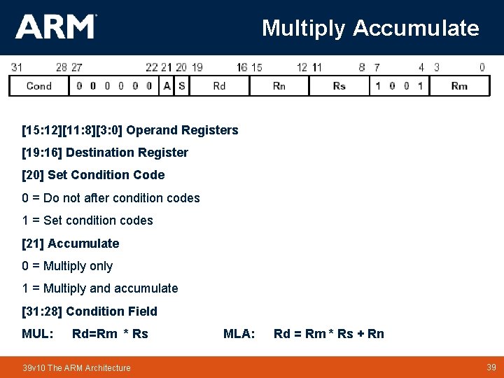
Multiply Accumulate [15: 12][11: 8][3: 0] Operand Registers [19: 16] Destination Register [20] Set Condition Code 0 = Do not after condition codes 1 = Set condition codes [21] Accumulate 0 = Multiply only 1 = Multiply and accumulate [31: 28] Condition Field MUL: Rd=Rm * Rs 39 v 10 The ARM Architecture MLA: Rd = Rm * Rs + Rn TM 39 39
Branch instructions n Branch : B{<cond>} label n Branch with Link : BL{<cond>} subroutine_label 31 28 27 Cond 25 24 23 0 1 L Offset Link bit 0 = Branch 1 = Branch with link Condition field n The processor core shifts the offset field left by 2 positions, sign-extends it and adds it to the PC n n ± 32 M byte range How to perform longer branches? 39 v 10 The ARM Architecture TM 40 40
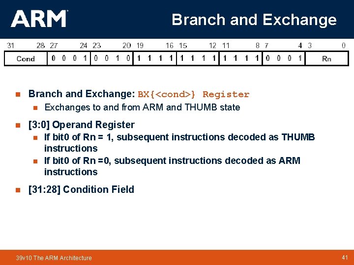
Branch and Exchange n Branch and Exchange: BX{<cond>} Register n n [3: 0] Operand Register n n n Exchanges to and from ARM and THUMB state If bit 0 of Rn = 1, subsequent instructions decoded as THUMB instructions If bit 0 of Rn =0, subsequent instructions decoded as ARM instructions [31: 28] Condition Field 39 v 10 The ARM Architecture TM 41 41
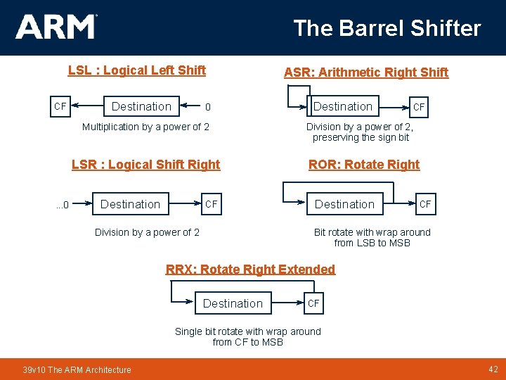
The Barrel Shifter LSL : Logical Left Shift CF Destination ASR: Arithmetic Right Shift Destination 0 Multiplication by a power of 2 Division by a power of 2, preserving the sign bit LSR : Logical Shift Right. . . 0 Destination CF ROR: Rotate Right Destination CF Division by a power of 2 CF Bit rotate with wrap around from LSB to MSB RRX: Rotate Right Extended Destination CF Single bit rotate with wrap around from CF to MSB 39 v 10 The ARM Architecture TM 42 42
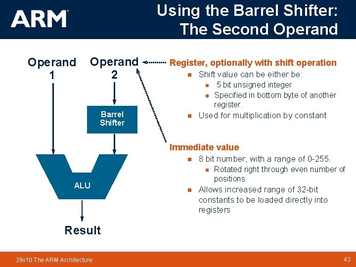
Using the Barrel Shifter: The Second Operand 1 Operand 2 Register, optionally with shift operation n Shift value can be either be: n n Barrel Shifter n 5 bit unsigned integer Specified in bottom byte of another register. Used for multiplication by constant Immediate value n 8 bit number, with a range of 0 -255. n ALU n Rotated right through even number of positions Allows increased range of 32 -bit constants to be loaded directly into registers Result 39 v 10 The ARM Architecture TM 43 43
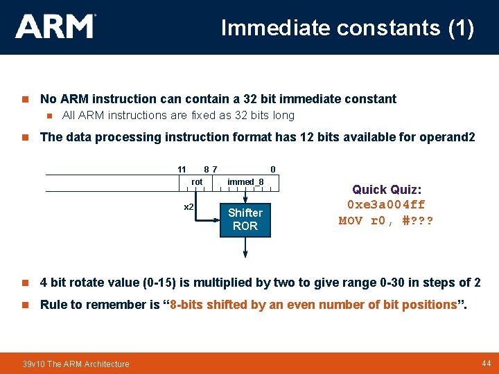
Immediate constants (1) n No ARM instruction can contain a 32 bit immediate constant n n All ARM instructions are fixed as 32 bits long The data processing instruction format has 12 bits available for operand 2 11 8 7 rot x 2 0 immed_8 Quick Quiz: 0 xe 3 a 004 ff MOV r 0, #? ? ? Shifter ROR n 4 bit rotate value (0 -15) is multiplied by two to give range 0 -30 in steps of 2 n Rule to remember is “ 8 -bits shifted by an even number of bit positions”. 39 v 10 The ARM Architecture TM 44 44
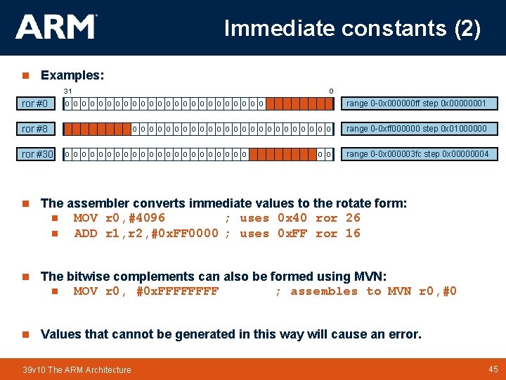
Immediate constants (2) n Examples: 31 ror #0 range 0 -0 x 000000 ff step 0 x 00000001 0 0 0 0 0 0 ror #8 ror #30 0 0 0 0 0 0 0 0 0 0 0 0 range 0 -0 xff 000000 step 0 x 01000000 range 0 -0 x 000003 fc step 0 x 00000004 n The assembler converts immediate values to the rotate form: n MOV r 0, #4096 ; uses 0 x 40 ror 26 n ADD r 1, r 2, #0 x. FF 0000 ; uses 0 x. FF ror 16 n The bitwise complements can also be formed using MVN: n MOV r 0, #0 x. FFFF ; assembles to MVN r 0, #0 n Values that cannot be generated in this way will cause an error. 39 v 10 The ARM Architecture TM 45 45
Loading 32 bit constants n To allow larger constants to be loaded, the assembler offers a pseudoinstruction: n LDR rd, =const n This will either: n Produce a MOV or MVN instruction to generate the value (if possible). or n n n Generate a LDR instruction with a PC-relative address to read the constant from a literal pool (Constant data area embedded in the code). For example n LDR r 0, =0 x. FF n LDR r 0, =0 x 5555 => => MOV r 0, #0 x. FF LDR r 0, [PC, #Imm 12] … … DCD 0 x 5555 This is the recommended way of loading constants into a register 39 v 10 The ARM Architecture TM 46 46
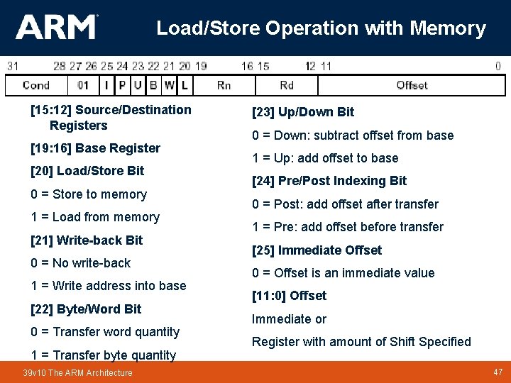
Load/Store Operation with Memory [15: 12] Source/Destination Registers [19: 16] Base Register [20] Load/Store Bit 0 = Store to memory 1 = Load from memory [21] Write-back Bit 0 = No write-back 1 = Write address into base [22] Byte/Word Bit 0 = Transfer word quantity 1 = Transfer byte quantity 39 v 10 The ARM Architecture [23] Up/Down Bit 0 = Down: subtract offset from base 1 = Up: add offset to base [24] Pre/Post Indexing Bit 0 = Post: add offset after transfer 1 = Pre: add offset before transfer [25] Immediate Offset 0 = Offset is an immediate value [11: 0] Offset Immediate or Register with amount of Shift Specified TM 47 47
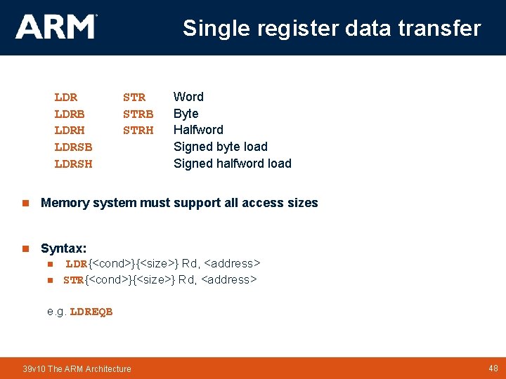
Single register data transfer LDRB LDRH LDRSB LDRSH STRB STRH Word Byte Halfword Signed byte load Signed halfword load n Memory system must support all access sizes n Syntax: n n LDR{<cond>}{<size>} Rd, <address> STR{<cond>}{<size>} Rd, <address> e. g. LDREQB 39 v 10 The ARM Architecture TM 48 48
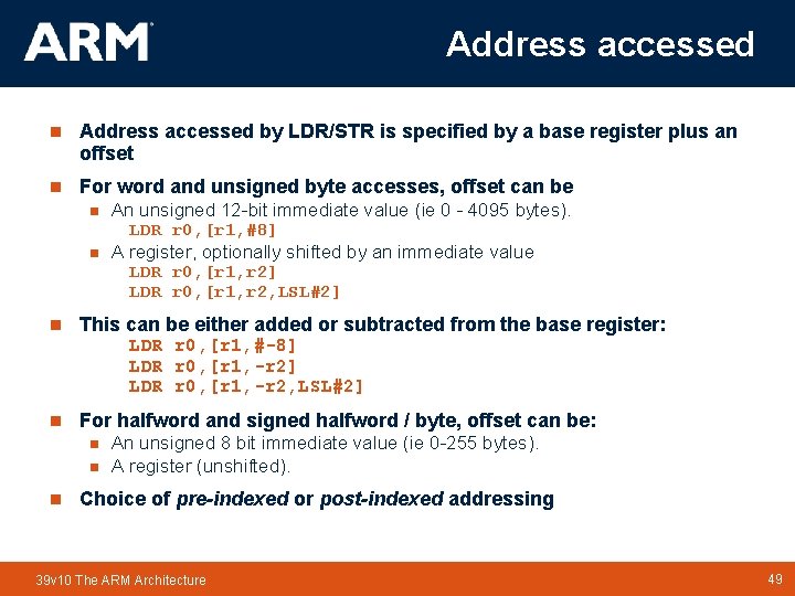
Address accessed n Address accessed by LDR/STR is specified by a base register plus an offset n For word and unsigned byte accesses, offset can be n An unsigned 12 -bit immediate value (ie 0 - 4095 bytes). LDR r 0, [r 1, #8] n A register, optionally shifted by an immediate value LDR r 0, [r 1, r 2] LDR r 0, [r 1, r 2, LSL#2] n This can be either added or subtracted from the base register: LDR r 0, [r 1, #-8] LDR r 0, [r 1, -r 2, LSL#2] n For halfword and signed halfword / byte, offset can be: n n n An unsigned 8 bit immediate value (ie 0 -255 bytes). A register (unshifted). Choice of pre-indexed or post-indexed addressing 39 v 10 The ARM Architecture TM 49 49
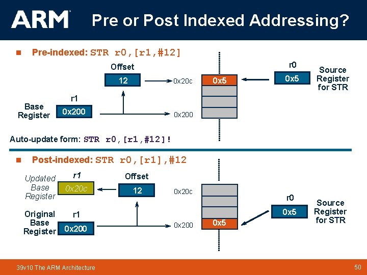
Pre or Post Indexed Addressing? n Pre-indexed: STR r 0, [r 1, #12] r 0 Offset 12 Base Register 0 x 5 0 x 20 c 0 x 5 Source Register for STR r 1 0 x 200 Auto-update form: STR r 0, [r 1, #12]! n Post-indexed: STR r 0, [r 1], #12 Updated Base Register Original Base Register r 1 Offset 0 x 20 c 12 0 x 20 c r 0 0 x 5 r 1 0 x 200 39 v 10 The ARM Architecture 0 x 5 0 x 200 TM Source Register for STR 50 50
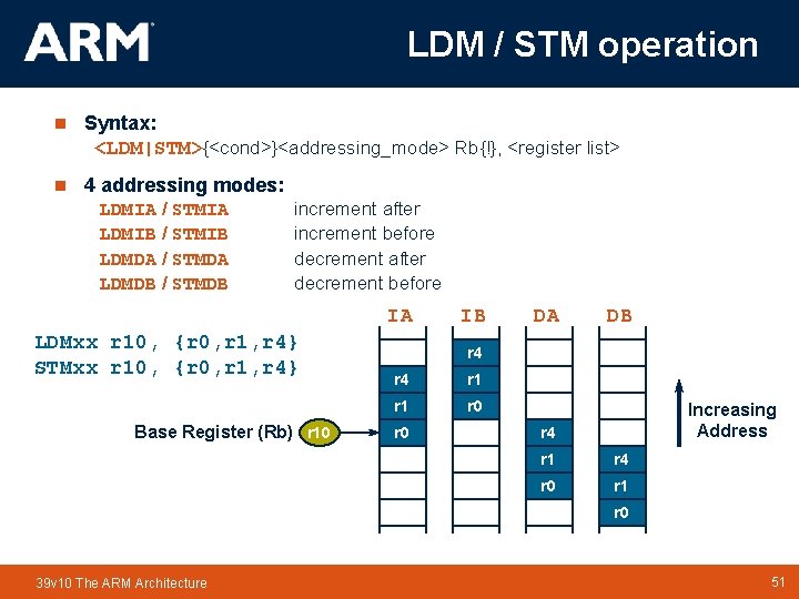
LDM / STM operation n Syntax: <LDM|STM>{<cond>}<addressing_mode> Rb{!}, <register list> n 4 addressing modes: LDMIA / STMIA LDMIB / STMIB LDMDA / STMDA LDMDB / STMDB increment after increment before decrement after decrement before IA LDMxx r 10, {r 0, r 1, r 4} STMxx r 10, {r 0, r 1, r 4} Base Register (Rb) r 10 IB DA DB r 4 r 1 r 0 Increasing Address r 4 r 1 r 4 r 0 r 1 r 0 39 v 10 The ARM Architecture TM 51 51
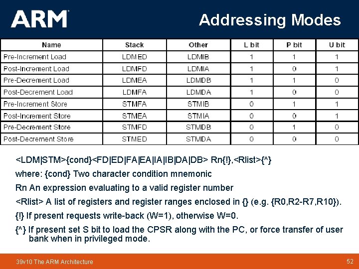
Addressing Modes <LDM|STM>{cond}<FD|ED|FA|EA|IA|IB|DA|DB> Rn{!}, <Rlist>{^} where: {cond} Two character condition mnemonic Rn An expression evaluating to a valid register number <Rlist> A list of registers and register ranges enclosed in {} (e. g. {R 0, R 2 -R 7, R 10}). {!} If present requests write-back (W=1), otherwise W=0. {^} If present set S bit to load the CPSR along with the PC, or force transfer of user bank when in privileged mode. 39 v 10 The ARM Architecture TM 52 52
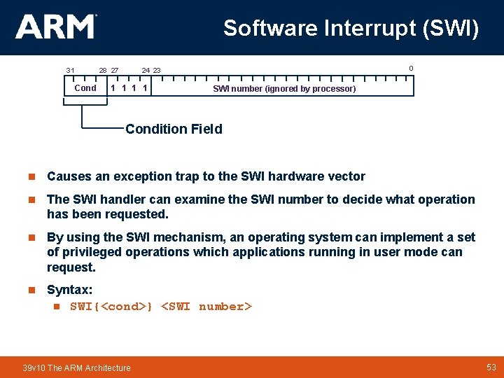
Software Interrupt (SWI) 31 28 27 Cond 0 24 23 1 1 SWI number (ignored by processor) Condition Field n Causes an exception trap to the SWI hardware vector n The SWI handler can examine the SWI number to decide what operation has been requested. n By using the SWI mechanism, an operating system can implement a set of privileged operations which applications running in user mode can request. n Syntax: n SWI{<cond>} <SWI number> 39 v 10 The ARM Architecture TM 53 53
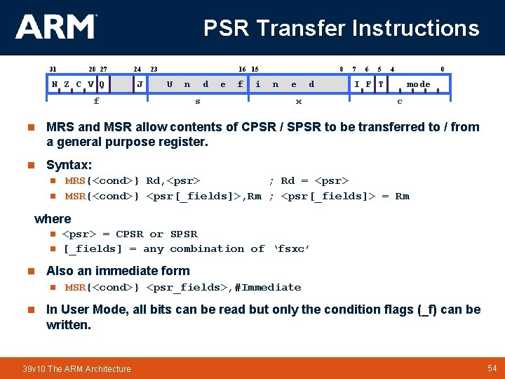
PSR Transfer Instructions 31 28 27 N Z C V Q 24 J 23 16 15 U n f d e f i 8 n e s d x 7 6 5 4 0 I F T mode c n MRS and MSR allow contents of CPSR / SPSR to be transferred to / from a general purpose register. n Syntax: n n MRS{<cond>} Rd, <psr> ; Rd = <psr> MSR{<cond>} <psr[_fields]>, Rm ; <psr[_fields]> = Rm where n n n Also an immediate form n n <psr> = CPSR or SPSR [_fields] = any combination of ‘fsxc’ MSR{<cond>} <psr_fields>, #Immediate In User Mode, all bits can be read but only the condition flags (_f) can be written. 39 v 10 The ARM Architecture TM 54 54
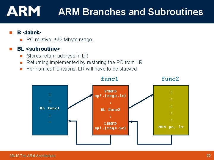
ARM Branches and Subroutines n B <label> n n PC relative. ± 32 Mbyte range. BL <subroutine> n n n Stores return address in LR Returning implemented by restoring the PC from LR For non-leaf functions, LR will have to be stacked func 1 func 2 : STMFD sp!, {regs, lr} : : : BL func 1 BL func 2 : : : LDMFD sp!, {regs, pc} 39 v 10 The ARM Architecture TM : : MOV pc, lr 55 55
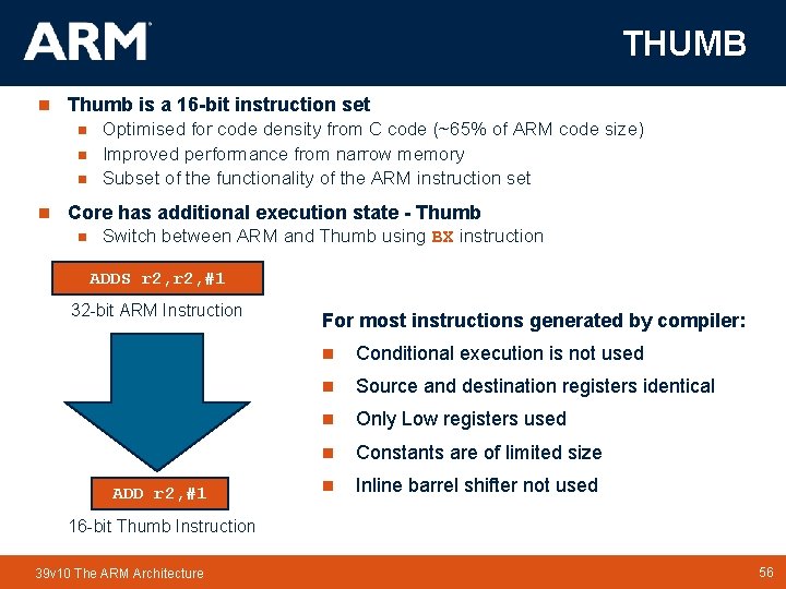
THUMB Thumb is a 16 -bit instruction set n n Optimised for code density from C code (~65% of ARM code size) Improved performance from narrow memory Subset of the functionality of the ARM instruction set Core has additional execution state - Thumb n n 31 Switch between ARM and Thumb using BX instruction ADDS r 2, #1 0 32 -bit ARM Instruction 15 ADD r 2, #1 0 For most instructions generated by compiler: n Conditional execution is not used n Source and destination registers identical n Only Low registers used n Constants are of limited size n Inline barrel shifter not used 16 -bit Thumb Instruction 39 v 10 The ARM Architecture TM 56 56
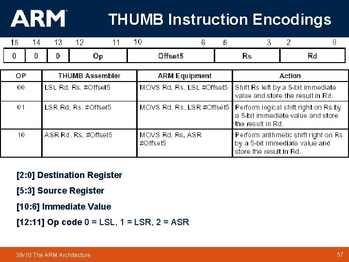
THUMB Instruction Encodings [2: 0] Destination Register [5: 3] Source Register [10: 6] Immediate Value [12: 11] Op code 0 = LSL, 1 = LSR, 2 = ASR 39 v 10 The ARM Architecture TM 57 57
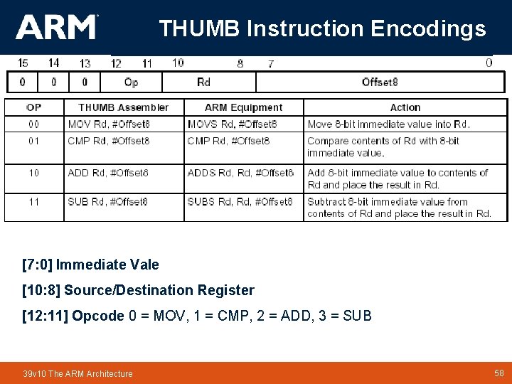
THUMB Instruction Encodings [7: 0] Immediate Vale [10: 8] Source/Destination Register [12: 11] Opcode 0 = MOV, 1 = CMP, 2 = ADD, 3 = SUB 39 v 10 The ARM Architecture TM 58 58
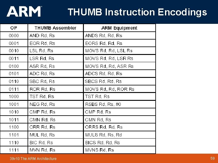
THUMB Instruction Encodings 39 v 10 The ARM Architecture TM 59 59
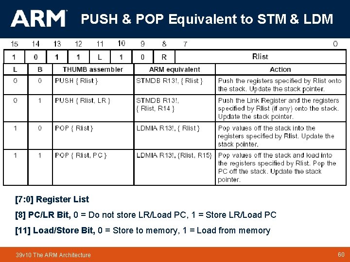
PUSH & POP Equivalent to STM & LDM [7: 0] Register List [8] PC/LR Bit, 0 = Do not store LR/Load PC, 1 = Store LR/Load PC [11] Load/Store Bit, 0 = Store to memory, 1 = Load from memory 39 v 10 The ARM Architecture TM 60 60
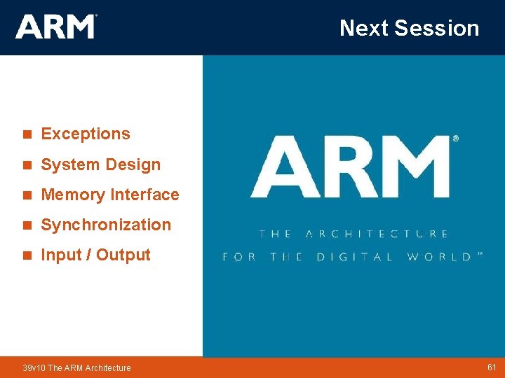
Next Session n Exceptions n System Design n Memory Interface n Synchronization n Input / Output 39 v 10 The ARM Architecture TM 61 61