EKT 121 4 DIGITAL ELECTRONICS I Chapter 3










- Slides: 123

EKT 121 / 4 DIGITAL ELECTRONICS I Chapter 3: Sequential Logic Circuits 1

“Combinational” vs “Sequential” n Combinational – outputs depend only on the inputs. – Do not have memory. – Cannot store state. n Sequential – outputs depend on inputs and past behavior. – Require use of storage elements. – Contents of storage elements is called “state”. – Circuit goes through sequence of states as a result of changes in inputs. 2

Overview of Sequential Circuits Storage Elements and Analysis – – – Introduction to sequential circuits Types of sequential circuits Storage elements § Latches § Flip-flops – Sequential circuit analysis § State tables § State diagrams 3

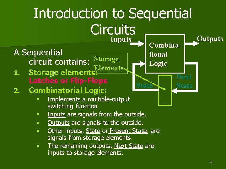
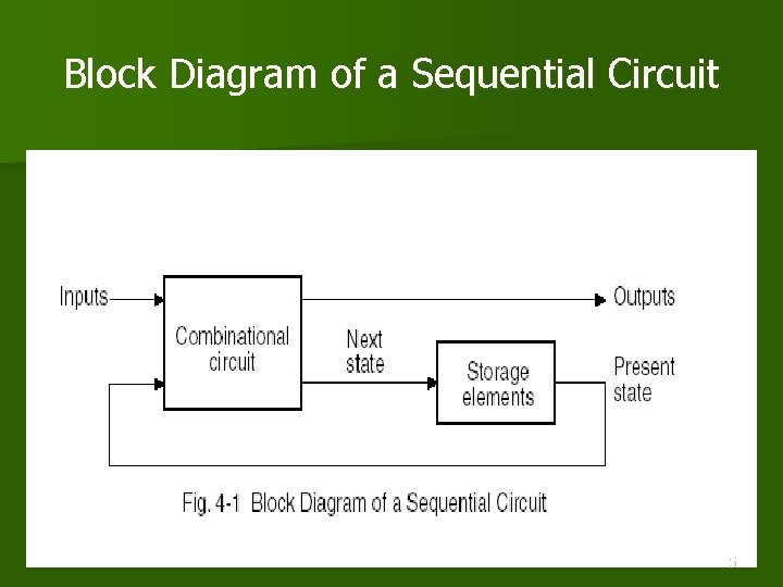
Introduction to Sequential Circuits Outputs Inputs A Sequential circuit contains: Storage 1. 2. Elements Storage elements: Latches or Flip-Flops Combinatorial Logic: § § § Combinational Logic State Next State Implements a multiple-output switching function Inputs are signals from the outside. Outputs are signals to the outside. Other inputs, State or Present State, are signals from storage elements. The remaining outputs, Next State are inputs to storage elements. 4

Block Diagram of a Sequential Circuit 5

Sequential Circuit Behaviour n Is determined from the inputs, outputs and present state. n The outputs and the next state are a function of the inputs and the present state. 6

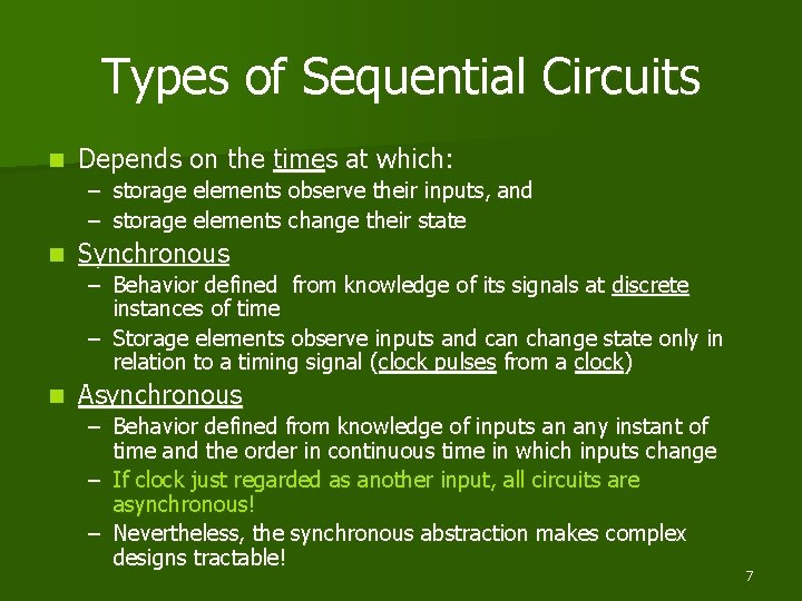
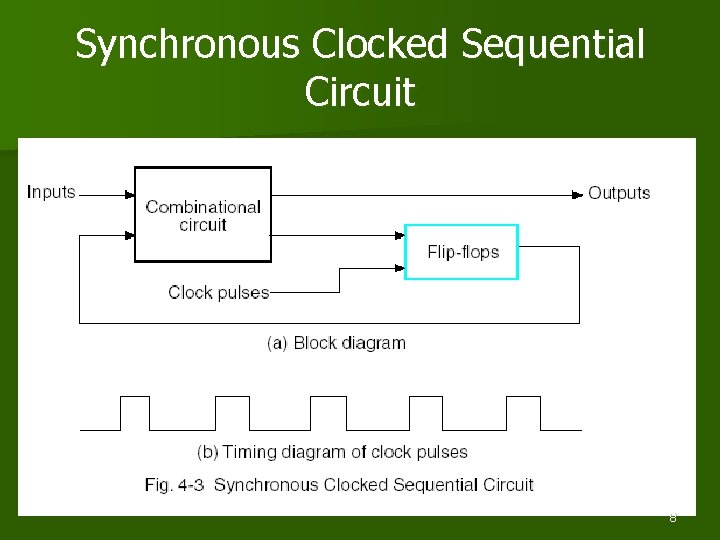
Types of Sequential Circuits n Depends on the times at which: – storage elements observe their inputs, and – storage elements change their state n Synchronous – Behavior defined from knowledge of its signals at discrete instances of time – Storage elements observe inputs and can change state only in relation to a timing signal (clock pulses from a clock) n Asynchronous – Behavior defined from knowledge of inputs an any instant of time and the order in continuous time in which inputs change – If clock just regarded as another input, all circuits are asynchronous! – Nevertheless, the synchronous abstraction makes complex designs tractable! 7

Synchronous Clocked Sequential Circuit 8

Sequential Circuit - Basic Function n The data stored in the “storage elements” defines the “state” of the sequential circuit at that time, i. e. present state. n The inputs, together with the present state of the storage elements, determine the outputs and the next state of the storage elements. 9

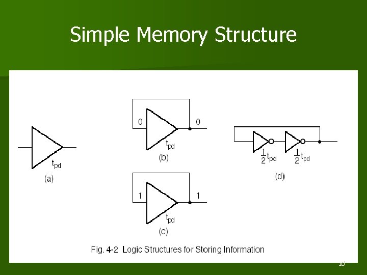
Simple Memory Structure 10

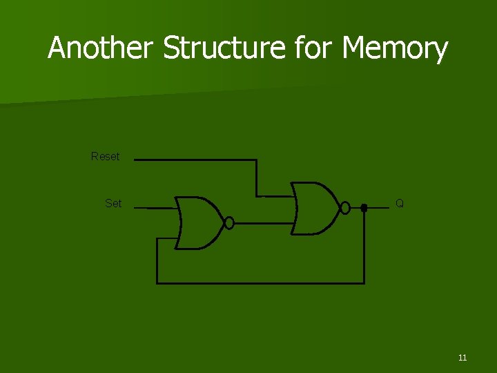
Another Structure for Memory Reset Set Q 11

The Most Common Memory Elements Used n Latches n Flip-flops – The basic single-bit memory elements, – With one or two inputs/outputs, – Designed using individual logic gates and feedback loops. – Both are referred to as “bistable elements” or “multivibrator”, i. e. having two stable states. 12

Latch vs Flip-flop n “The inputs, together with the present state of the storage elements, determine the outputs and the next state of the storage elements. ” n Latch – Asynchronous. – Change of state can happen at any time, whenever its inputs change. n Flip-Flops – Synchronous. – Change of state occurs only at specific times determined by a clock pulse input. – Flip-flops are constructed from latches!! 13

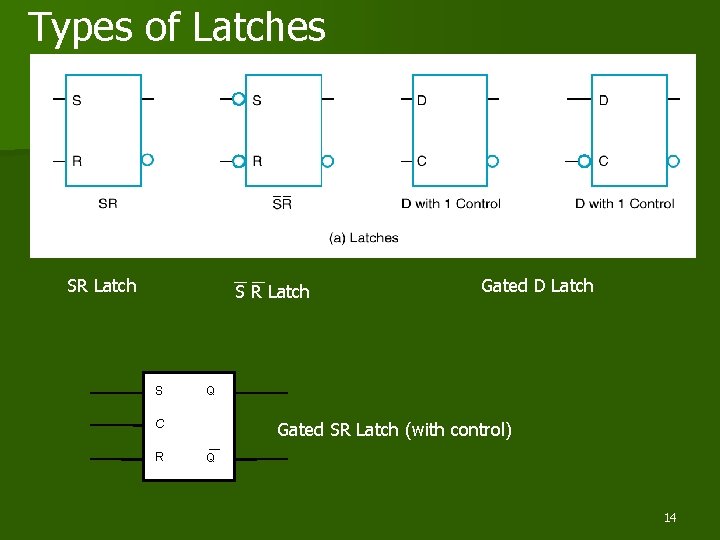
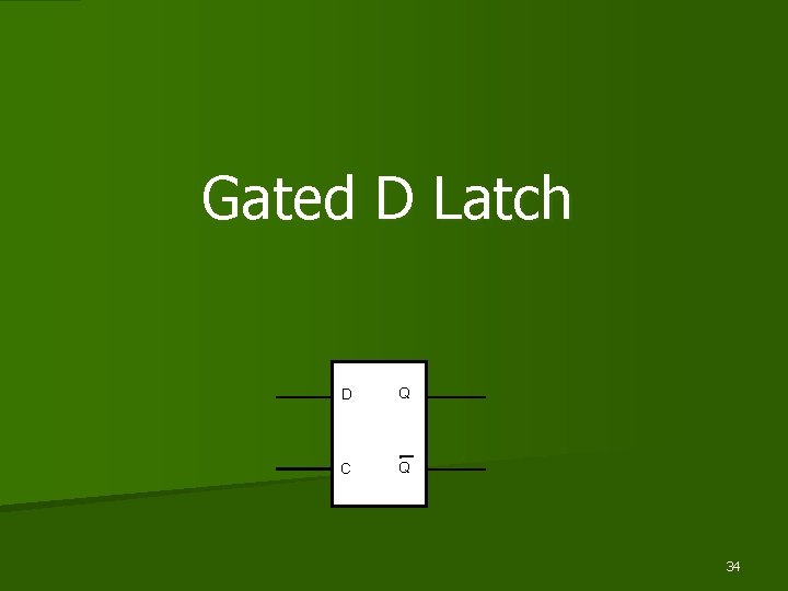
Types of Latches SR Latch S Q C R Gated D Latch Gated SR Latch (with control) Q 14

S R Latch 15

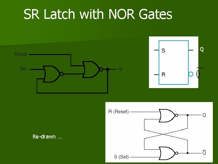
SR Latch with NOR Gates Q Reset Set Q Re-drawn … 16

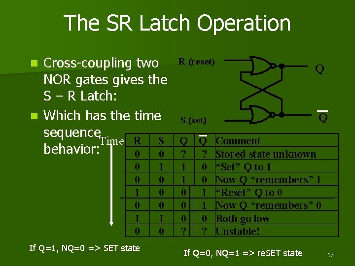
The SR Latch Operation Cross-coupling two NOR gates gives the S – R Latch: n Which has the time sequence Time R S behavior: 0 0 n 0 0 1 0 If Q=1, NQ=0 => SET state 1 0 0 0 1 0 R (reset) Q Q S (set) Q ? 1 1 0 0 0 ? Q ? 0 0 1 1 0 ? Comment Stored state unknown “Set” Q to 1 Now Q “remembers” 1 “Reset” Q to 0 Now Q “remembers” 0 Both go low Unstable! If Q=0, NQ=1 => re. SET state 17

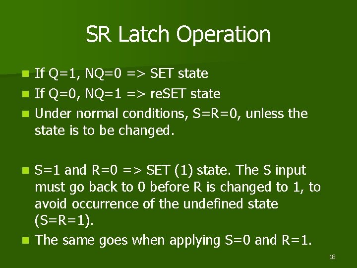
SR Latch Operation If Q=1, NQ=0 => SET state n If Q=0, NQ=1 => re. SET state n Under normal conditions, S=R=0, unless the state is to be changed. n S=1 and R=0 => SET (1) state. The S input must go back to 0 before R is changed to 1, to avoid occurrence of the undefined state (S=R=1). n The same goes when applying S=0 and R=1. n 18

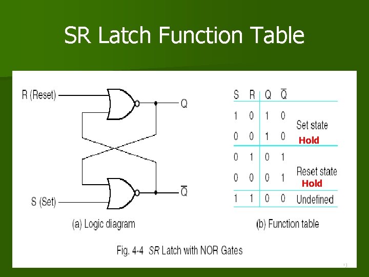
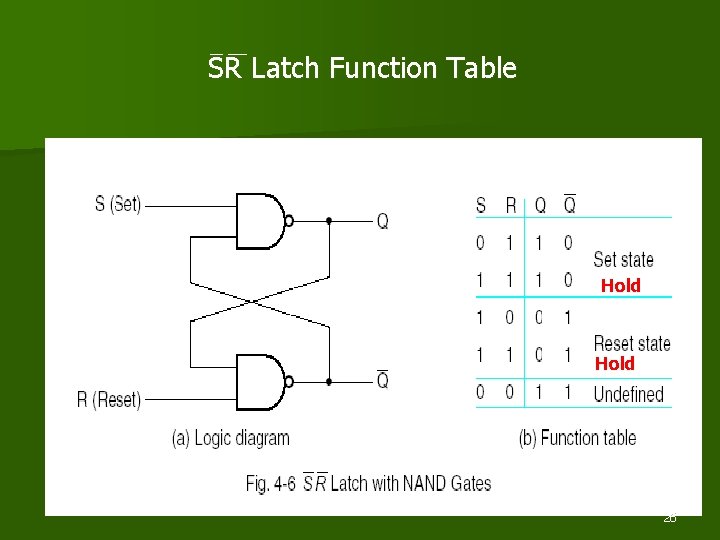
SR Latch Function Table Hold 19

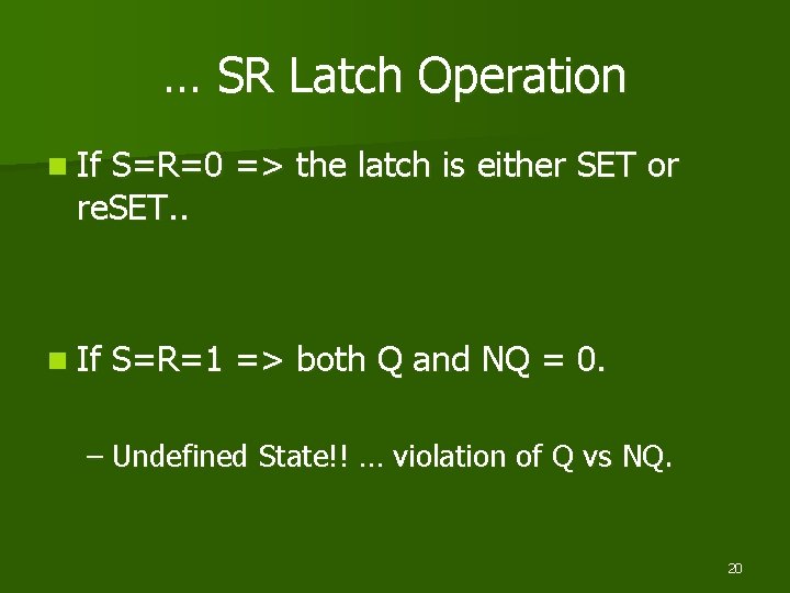
… SR Latch Operation n If S=R=0 => the latch is either SET or re. SET. . n If S=R=1 => both Q and NQ = 0. – Undefined State!! … violation of Q vs NQ. 20

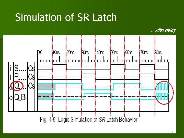
Simulation of SR Latch. . with delay 21

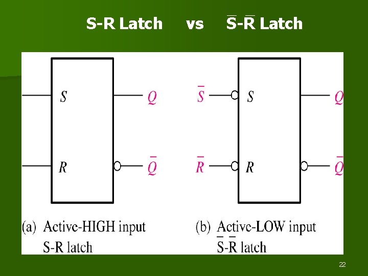
S-R Latch vs S-R Latch 22

S R Latch 23

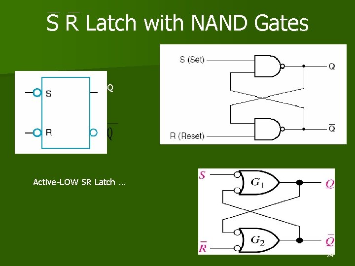
S R Latch with NAND Gates Q Active-LOW SR Latch … 24

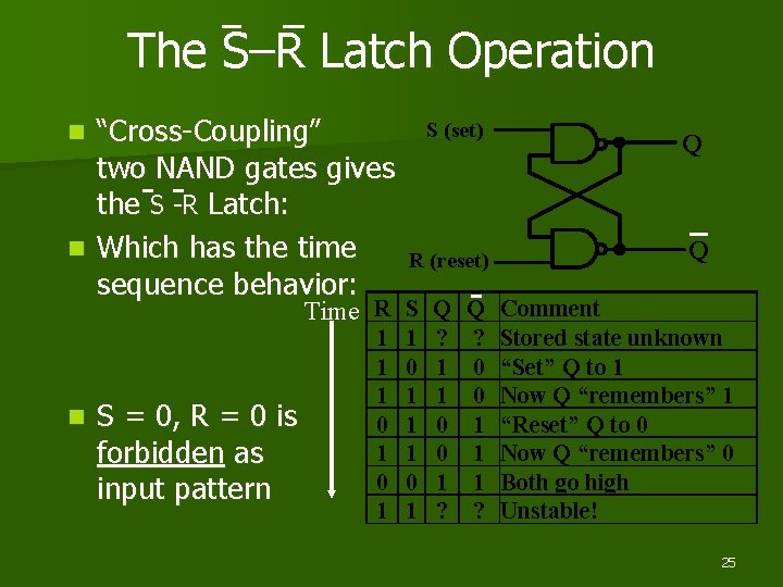
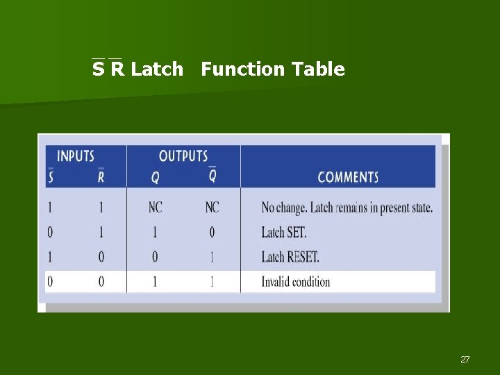
The S–R Latch Operation “Cross-Coupling” two NAND gates gives the S -R Latch: n Which has the time sequence behavior: S (set) n Q Q R (reset) Time R S Q Q Comment n S = 0, R = 0 is forbidden as input pattern 1 1 1 0 1 ? 1 1 0 0 1 ? ? 0 0 1 1 1 ? Stored state unknown “Set” Q to 1 Now Q “remembers” 1 “Reset” Q to 0 Now Q “remembers” 0 Both go high Unstable! 25

SR Latch Function Table Hold 26

S R Latch Function Table 27

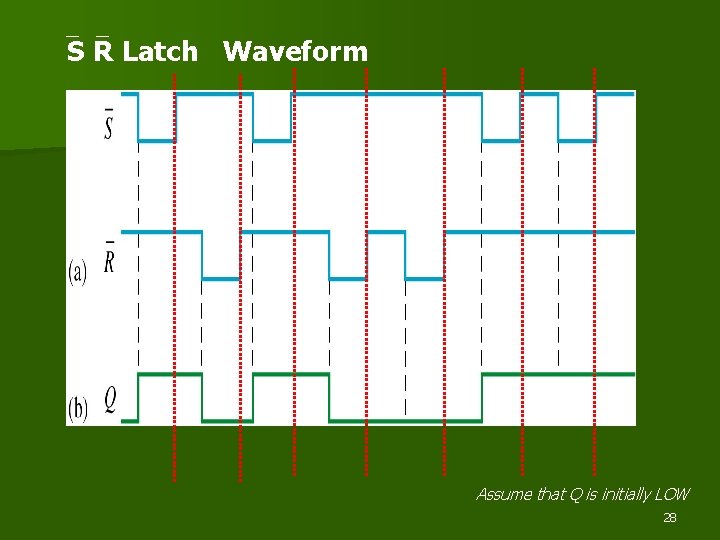
S R Latch Waveform 1 2 3 4 5 6 7 Assume that Q is initially LOW 28

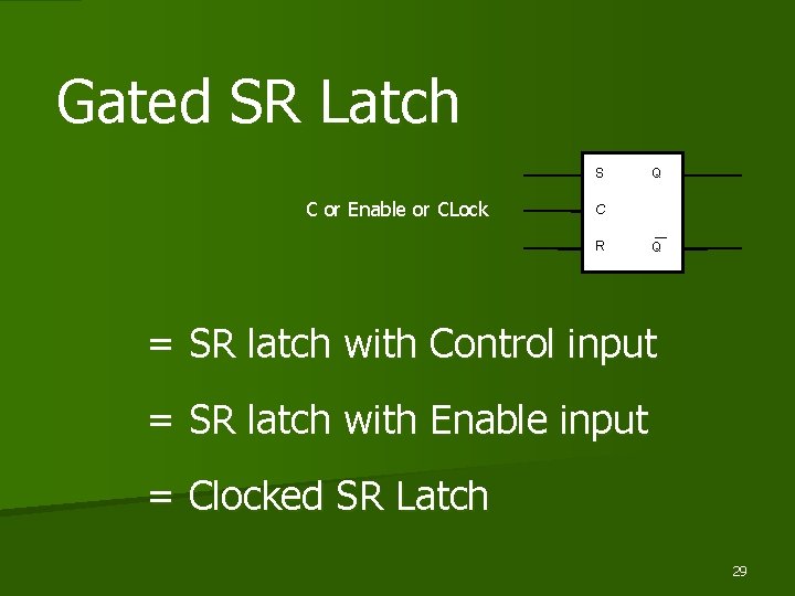
Gated SR Latch S C or Enable or CLock Q C R Q = SR latch with Control input = SR latch with Enable input = Clocked SR Latch 29

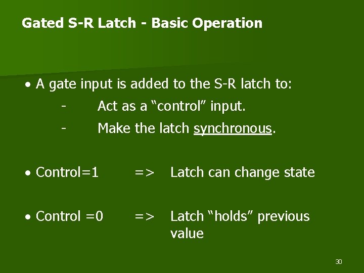
Gated S-R Latch - Basic Operation · A gate input is added to the S-R latch to: - Act as a “control” input. - Make the latch synchronous. · Control=1 => Latch can change state · Control =0 => Latch “holds” previous value 30

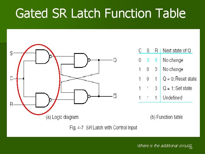
Gated SR Latch Function Table Where is the additional circuit? 31

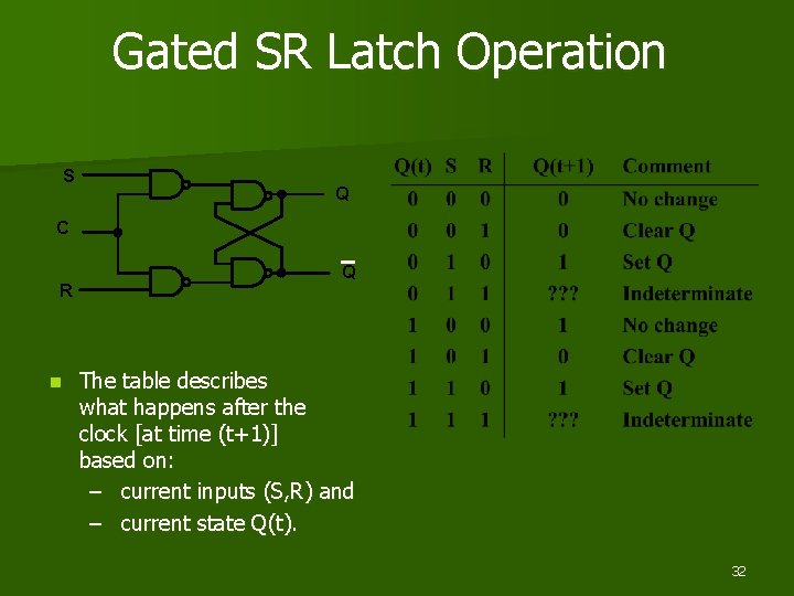
Gated SR Latch Operation S Q C R n Q The table describes what happens after the clock [at time (t+1)] based on: – current inputs (S, R) and – current state Q(t). 32

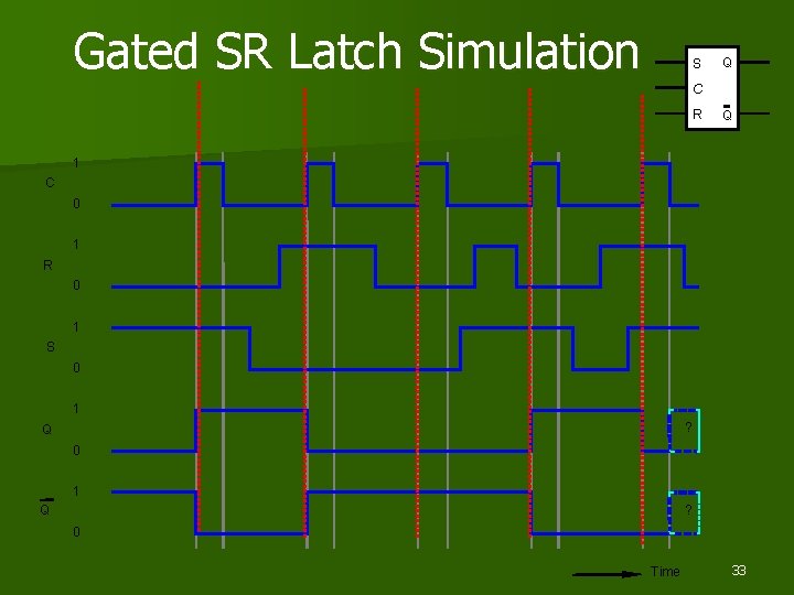
Gated SR Latch Simulation S Q C R Q 1 C 0 1 R 0 1 S 0 1 ? Q 0 Time 33

Gated D Latch D Q C Q 34

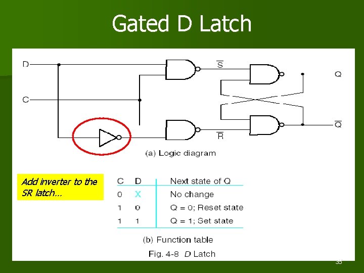
Gated D Latch Add inverter to the SR latch… 35

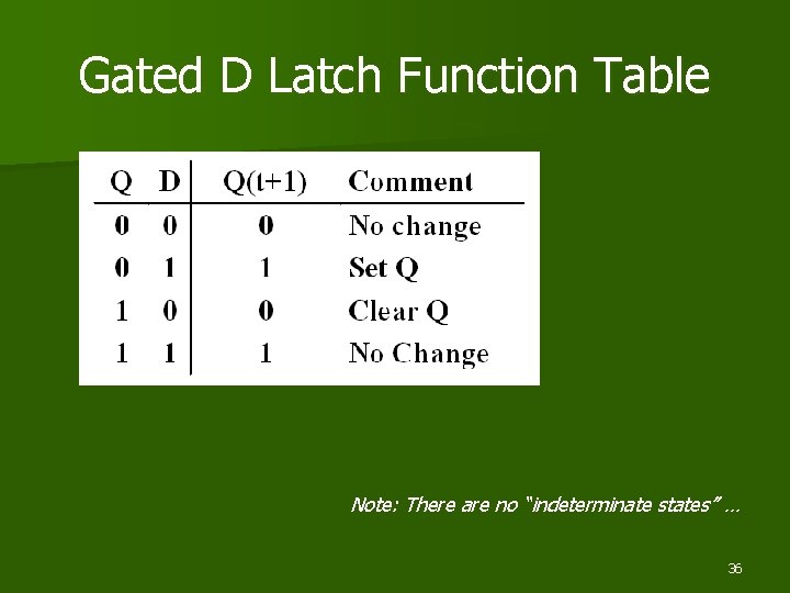
Gated D Latch Function Table Note: There are no “indeterminate states” … 36

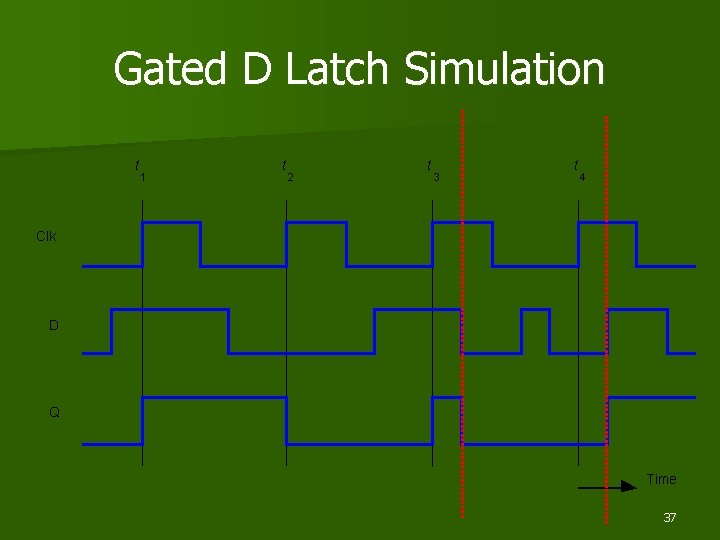
Gated D Latch Simulation t 1 t 2 t 3 t 4 Clk D Q Time 37

State Change in Latch n Change in latch state => Trigger n The D latch with clock pulses on its Control, C, input is triggered every time a pulse to logic-1 level occurs. n As long as the pulse remains at the logic-1 level, any changes in the data input will change the state of the latch. “Level” triggered 38

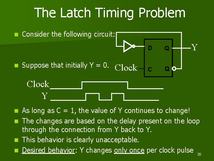
The Latch Timing Problem n n Consider the following circuit: Suppose that initially Y = 0. Clock D Q C Q Y Clock Y n n As long as C = 1, the value of Y continues to change! The changes are based on the delay present on the loop through the connection from Y back to Y. This behavior is clearly unacceptable. Desired behavior: Y changes only once per clock pulse 39

Solution to the Latch Timing Problem – Use latch to form flip-flop n Replace the clocked D-latch with: – A Master-slave Flip-flop § Two stage § Output does not change until clock is disabled – An Edge-triggered Flip-flop § Triggers only during a signal transition on the clock, either from 1 to 0 or from 0 to 1, and is disabled at all other times. 40

Master-Slave Flip-flops SR JK D 41

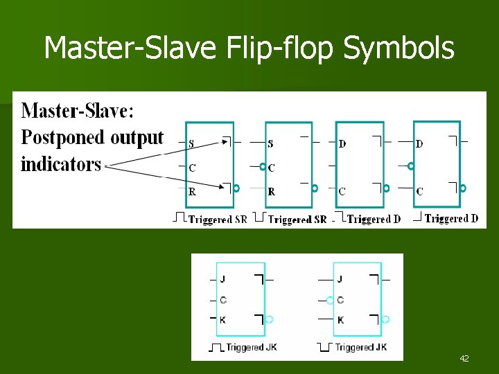
Master-Slave Flip-flop Symbols 42

Master-Slave Flip-flops n Is pulse (level)-triggered. n Data is entered into the flip-flop at the leading edge of the clock pulses, but the output is only reflected at the trailing edge. n Does not allow data to change while the clock pulse is still active. …. Either the Master or the Slave is enabled, not both 43

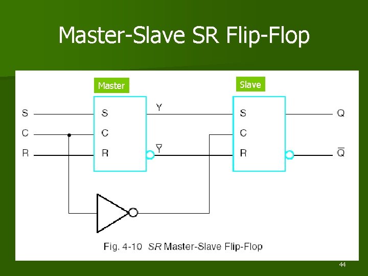
Master-Slave SR Flip-Flop Master Slave 44

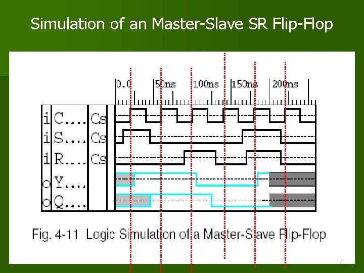
Master-Slave SR Flip-Flop n When C=0, the output of the inverter is 1 => the slave latch is enabled, and its output, Q, is equal to the master output, Y. The master latch is disabled because C=0. n When a logic-1 pulse is applied to C, the values on S and R control the stored value in the master latch, Y. The slave at this time is disabled, because its C input is 0. n Any changes in the S and R inputs change the master output, Y, but cannot affect the slave output, Q. n When the pulse returns to 0, the master is disabled and is isolated from the S and R inputs. At the same time, the slave is enabled, and the current value of Y is transferred to the output of the flip-flop at Q. 45

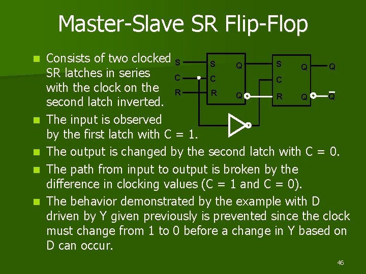
Master-Slave SR Flip-Flop n n n Consists of two clocked S S S Q Q Q SR latches in series C C C with the clock on the R R Q Q second latch inverted. The input is observed by the first latch with C = 1. The output is changed by the second latch with C = 0. The path from input to output is broken by the difference in clocking values (C = 1 and C = 0). The behavior demonstrated by the example with D driven by Y given previously is prevented since the clock must change from 1 to 0 before a change in Y based on D can occur. 46

Simulation of an Master-Slave SR Flip-Flop 47

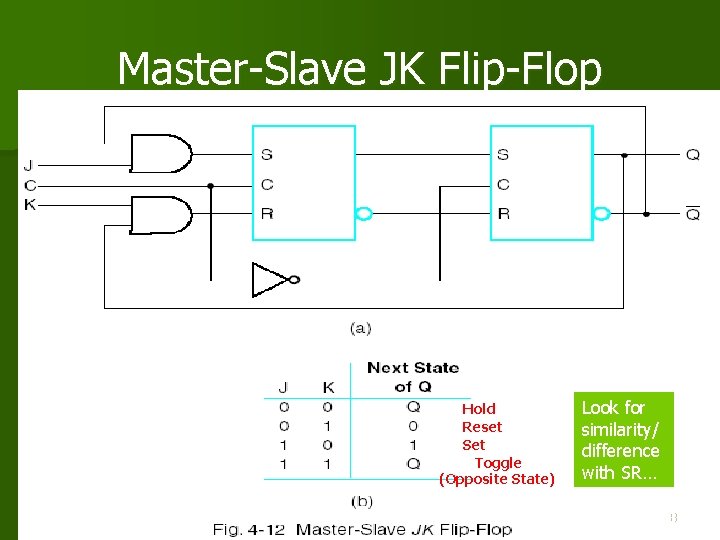
Master-Slave JK Flip-Flop Hold Reset Set Toggle (Opposite State) Look for similarity/ difference with SR… 48

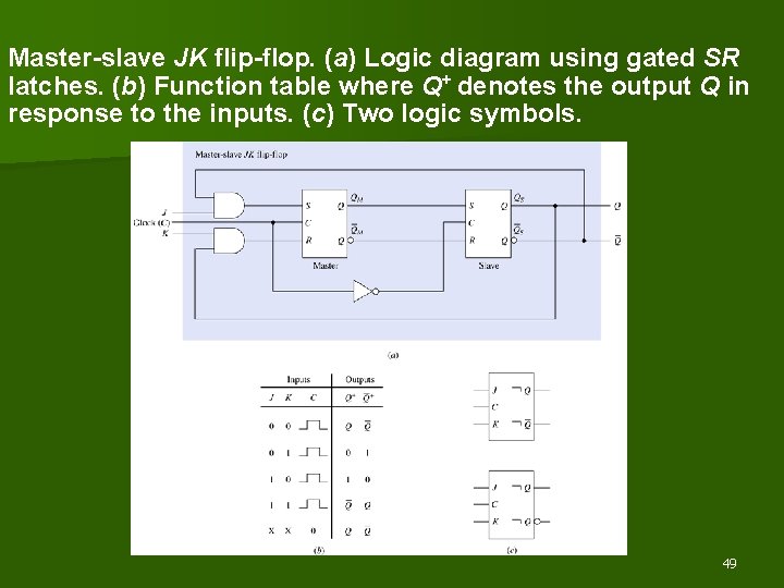
Master-slave JK flip-flop. (a) Logic diagram using gated SR latches. (b) Function table where Q+ denotes the output Q in response to the inputs. (c) Two logic symbols. 49

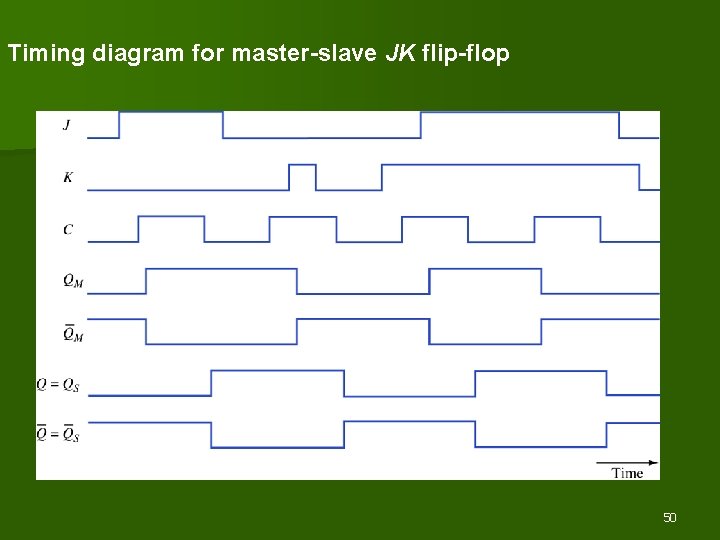
Timing diagram for master-slave JK flip-flop 50

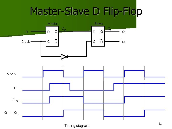
Master-Slave D Flip-Flop Master D Clock D Q C Q Slave Qm D Q C Q Qs Q Q Clock D Qm Q = Qs Timing diagram 51

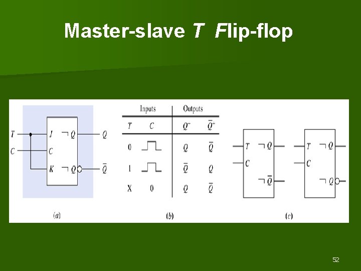
Master-slave T Flip-flop 52

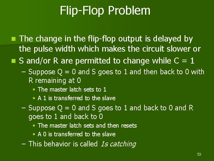
Flip-Flop Problem The change in the flip-flop output is delayed by the pulse width which makes the circuit slower or n S and/or R are permitted to change while C = 1 n – Suppose Q = 0 and S goes to 1 and then back to 0 with R remaining at 0 § § The master latch sets to 1 A 1 is transferred to the slave – Suppose Q = 0 and S goes to 1 and back to 0 and R goes to 1 and back to 0 § The master latch sets and then resets § A 0 is transferred to the slave – This behavior is called 1 s catching 53

Flip-Flop Solution n Use edge-triggering instead of master-slave. n An edge-triggered flip-flop ignores the pulse while it is at a constant level and triggers only during a transition of the clock signal. 1. Edge-triggered flip-flops can be built directly at the electronic circuit level, or 2. A master-slave D flip-flop which also exhibits edgetriggered behavior can be used. 54

Edge-Triggered Flip-flops n Flip-flops are synchronous bistable devices. n Synchronous: because the output changes state ony at a certain point on a triggering input, i. e. CLK, which is the control input. n Edge-triggered flip-flop: changes state at either the positive edge (rising edge) or at the negative edge (falling edge) of the cock pulse. 55

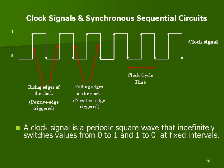
Clock Signals & Synchronous Sequential Circuits 1 Clock signal 0 Rising edges of the clock (Positive-edge triggered) n Falling edges of the clock (Negative-edge triggered) Clock Cycle Time A clock signal is a periodic square wave that indefinitely switches values from 0 to 1 and 1 to 0 at fixed intervals. 56

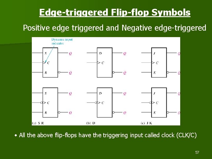
Edge-triggered Flip-flop Symbols Positive edge triggered and Negative edge-triggered • All the above flip-flops have the triggering input called clock (CLK/C) 57

Edge-Triggered Flip-flops n SR flip-flop n JK flip-flop n. D flip-flop n. T flip-flop 58

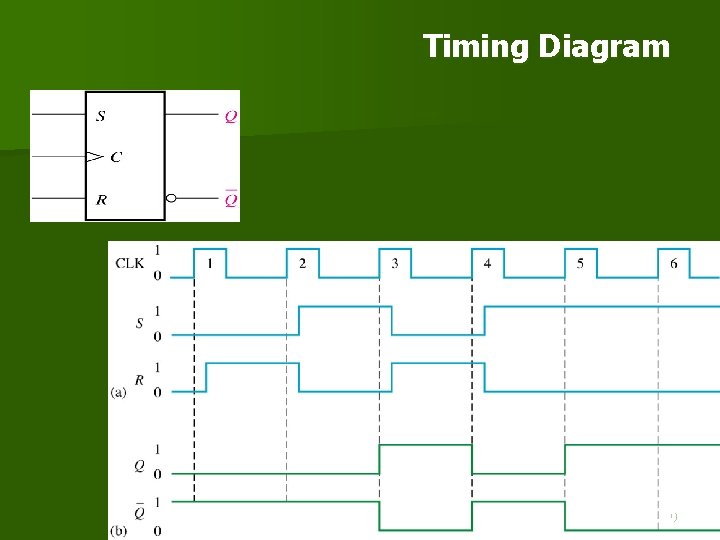
Timing Diagram 59

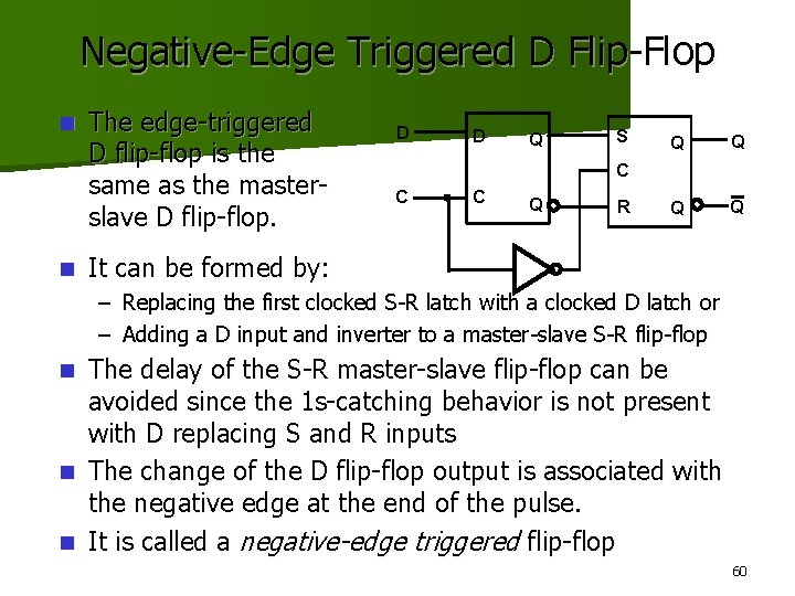
Negative-Edge Triggered D Flip-Flop n n The edge-triggered D flip-flop is the same as the masterslave D flip-flop. D D Q S Q Q C C C Q R It can be formed by: – Replacing the first clocked S-R latch with a clocked D latch or – Adding a D input and inverter to a master-slave S-R flip-flop The delay of the S-R master-slave flip-flop can be avoided since the 1 s-catching behavior is not present with D replacing S and R inputs n The change of the D flip-flop output is associated with the negative edge at the end of the pulse. n It is called a negative-edge triggered flip-flop n 60

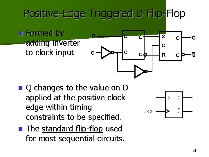
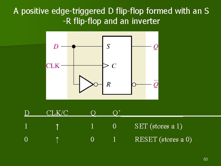
Positive-Edge Triggered D Flip-Flop n Formed by adding inverter to clock input D D S Q Q Q C C C Q changes to the value on D applied at the positive clock edge within timing constraints to be specified. n The standard flip-flop used for most sequential circuits. Q R n D Clock Q Q 61

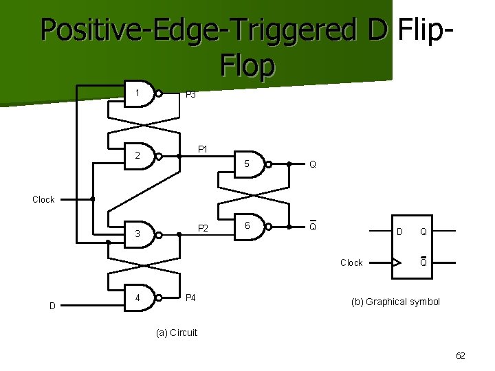
Positive-Edge-Triggered D Flip. Flop 1 P 3 P 1 2 5 Q 6 Q Clock P 2 3 D Clock D 4 P 4 Q Q (b) Graphical symbol (a) Circuit 62

A positive edge-triggered D flip-flop formed with an S -R flip-flop and an inverter D CLK/C Q Q’_________ 1 ↑ 1 0 SET (stores a 1) 0 ↑ 0 1 RESET (stores a 0) 63

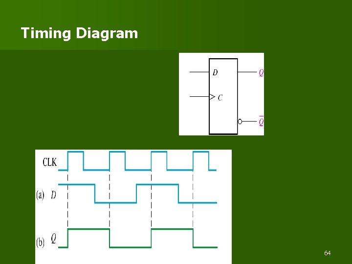
Timing Diagram 64

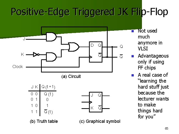
Positive-Edge Triggered JK Flip-Flop Not used much anymore in VLSI n Advantageous only if using FF chips n A real case of “learning the hard stuff just because the lecturer wants to make things hard for you” n J D K Q Q Clock (a) Circuit J K Q ( t + 1) 0 0 1 1 0 1 Q (t ) (b) Truth table J Q K Q (c) Graphical symbol 65

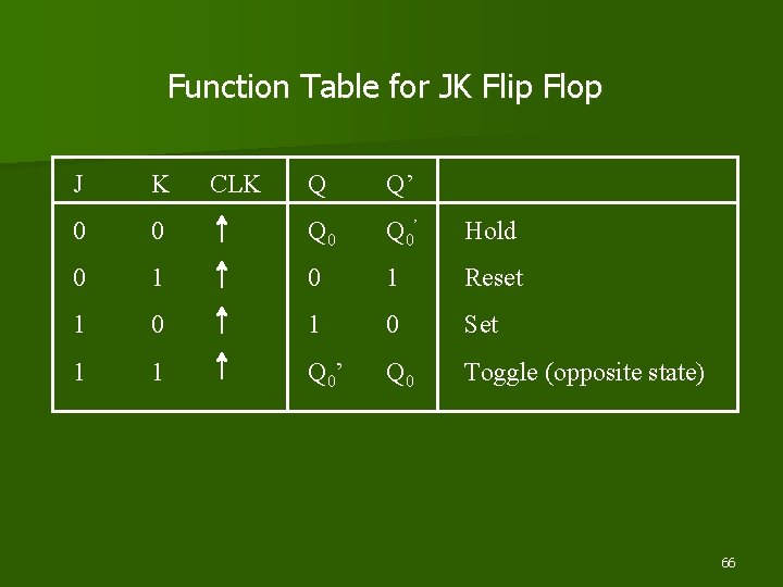
Function Table for JK Flip Flop J K 0 CLK Q Q’ 0 Q 0’ Hold 0 1 Reset 1 0 Set 1 1 Q 0’ Q 0 Toggle (opposite state) 66

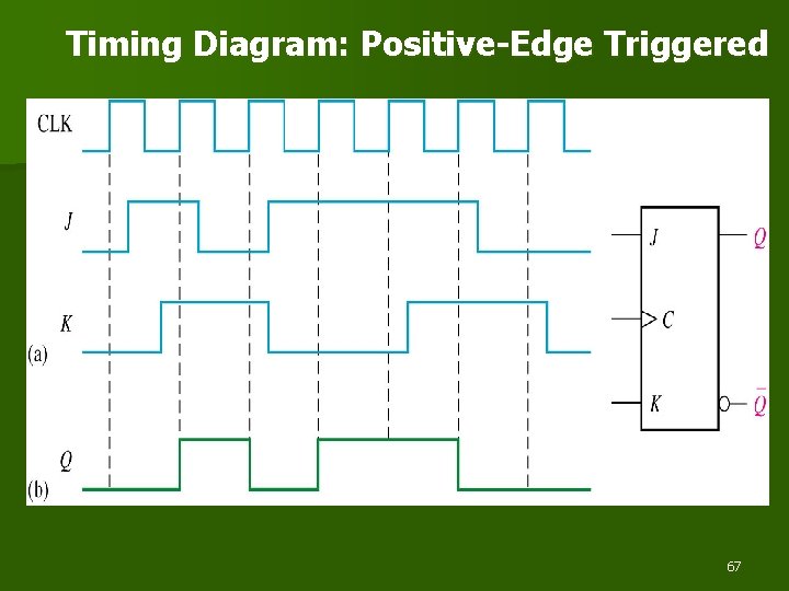
Timing Diagram: Positive-Edge Triggered 67

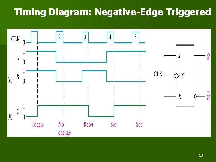
Timing Diagram: Negative-Edge Triggered 68

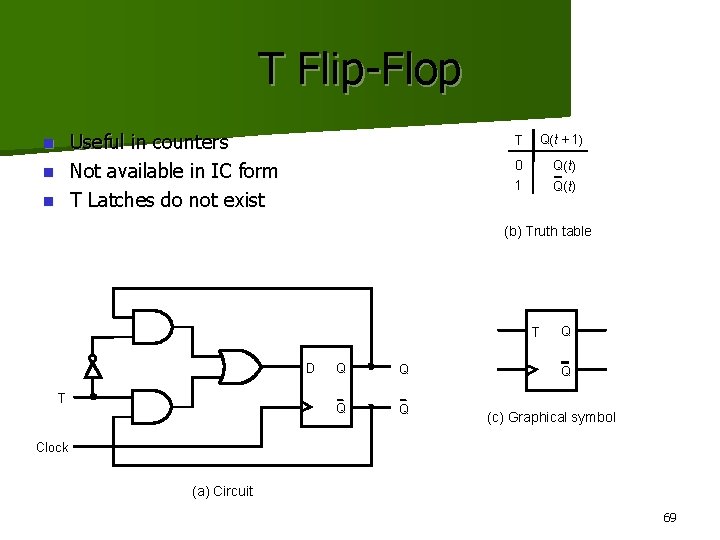
T Flip-Flop Useful in counters n Not available in IC form n T Latches do not exist n T Q( t + 1) 0 Q( t ) 1 Q( t ) (b) Truth table T D T Q Q Q (c) Graphical symbol Clock (a) Circuit 69

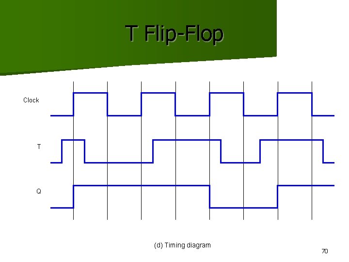
T Flip-Flop Clock T Q (d) Timing diagram 70

D latch vs D flip-flop 71

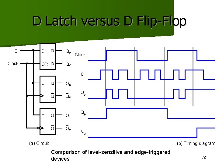
D Latch versus D Flip-Flop D Clock Q Qa Clk Q Qa D Clock D D D Q Qb Q Qc Q a Q b Q c (a) Circuit (b) Timing diagram Comparison of level-sensitive and edge-triggered devices 72

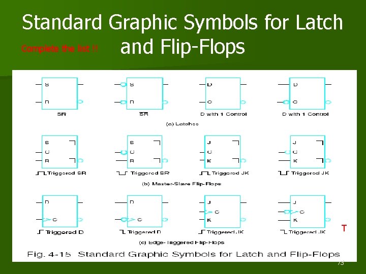
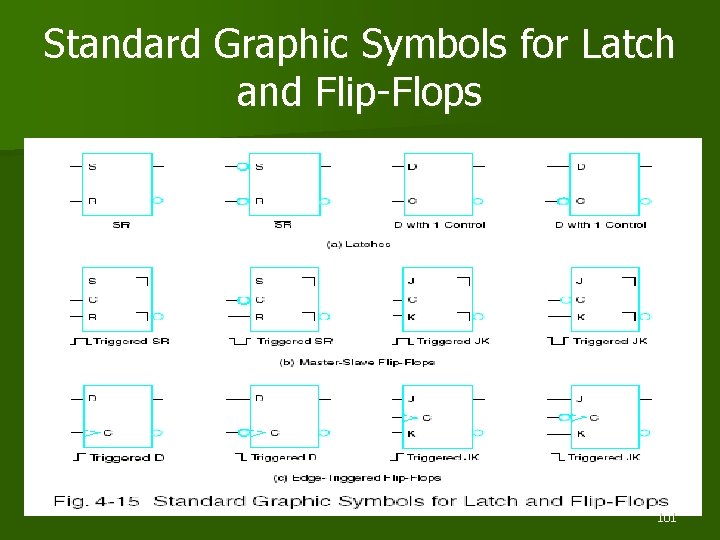
Standard Graphic Symbols for Latch Complete the list !! and Flip-Flops T 73

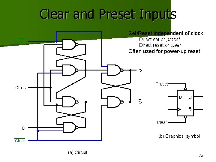
Direct Inputs Preset (Set) & Clear (Re. Set) 74

Clear and Preset Inputs Set/Reset independent of clock Direct set or preset Direct reset or clear Preset Often used for power-up reset Q Preset Clock D Q Q Q Clear D (b) Graphical symbol Clear (a) Circuit 75

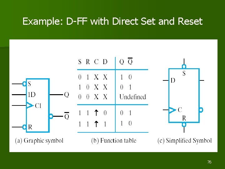
Example: D-FF with Direct Set and Reset 76

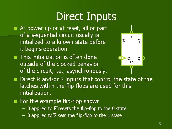
Direct Inputs n n At power up or at reset, all or part of a sequential circuit usually is S D Q initialized to a known state before it begins operation This initialization is often done C Q R outside of the clocked behavior of the circuit, i. e. , asynchronously. Direct R and/or S inputs that control the state of the latches within the flip-flops are used for this initialization. For the example flip-flop shown – 0 applied to R resets the flip-flop to the 0 state – 0 applied to S sets the flip-flop to the 1 state 77

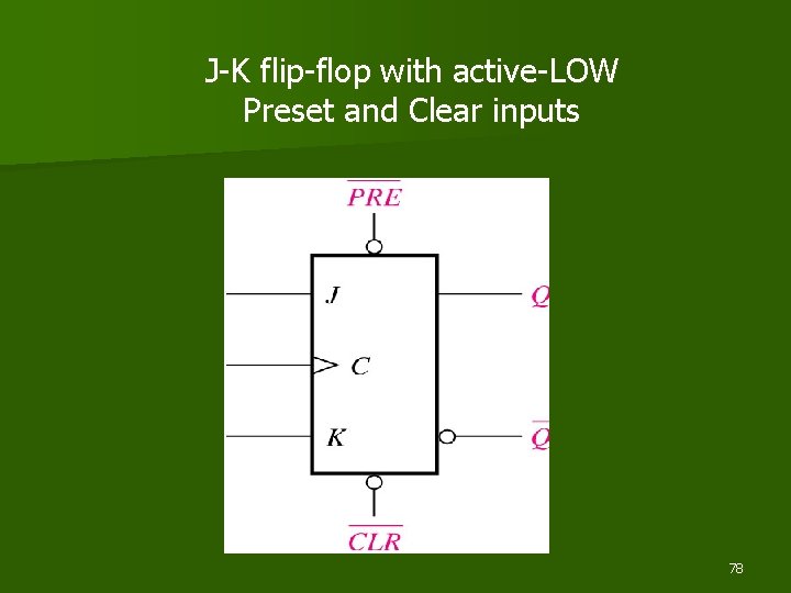
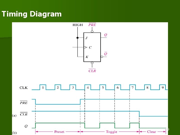
J-K flip-flop with active-LOW Preset and Clear inputs 78

Timing Diagram 79

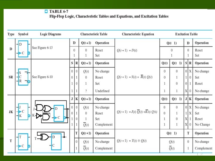
State Diagram, Excitation Table, Characteristic Equation 80

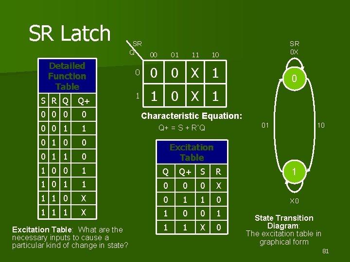
SR Latch Detailed Function Table 10 SR 0 X 0 0 0 X 1 0 1 1 0 X 1 SR Q 00 01 11 S R Q Q+ 0 0 0 1 1 0 0 1 Q 1 0 1 1 0 0 0 X 1 1 0 X 0 1 1 1 X 1 0 0 1 1 1 X 0 Excitation Table: What are the necessary inputs to cause a particular kind of change in state? Characteristic Equation: 01 Q+ = S + R’Q 10 Excitation Table Q+ S R 1 X 0 State Transition Diagram: The excitation table in graphical form 81

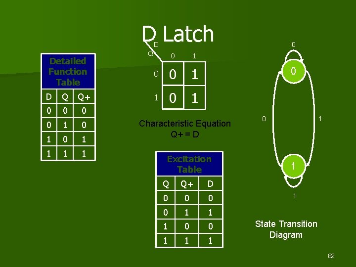
D Latch D Detailed Function Table D Q Q+ 0 0 1 0 1 1 Q 0 0 1 1 0 Characteristic Equation Q+ = D Excitation Table Q Q+ D 0 0 1 1 1 State Transition Diagram 82

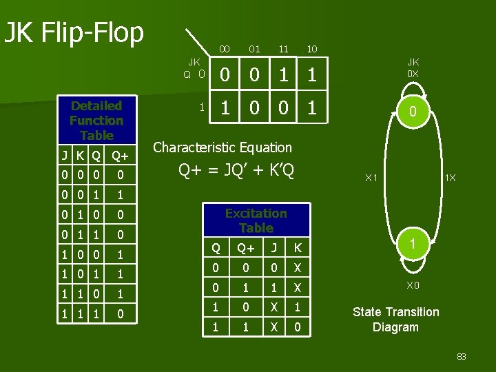
JK Flip-Flop 00 JK Q 0 Detailed Function Table J K Q Q+ 0 0 0 1 1 0 1 1 1 1 0 1 01 11 10 JK 0 X 0 0 1 1 1 0 0 1 0 Characteristic Equation Q+ = JQ’ + K’Q X 1 1 X Excitation Table Q Q+ J K 0 0 0 X 0 1 1 X 1 0 X 1 1 1 X 0 State Transition Diagram 83

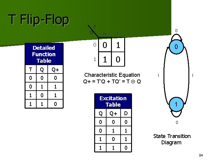
T Flip-Flop T Q Detailed Function Table T Q Q+ 0 0 1 1 1 0 0 Characteristic Equation Q+ = T’Q + TQ’ = T Q Excitation Table Q Q+ D 0 0 1 1 1 0 State Transition Diagram 84

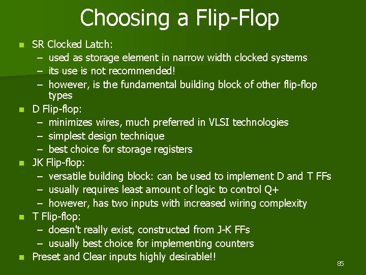
Choosing a Flip-Flop n n n SR Clocked Latch: – used as storage element in narrow width clocked systems – its use is not recommended! – however, is the fundamental building block of other flip-flop types D Flip-flop: – minimizes wires, much preferred in VLSI technologies – simplest design technique – best choice for storage registers JK Flip-flop: – versatile building block: can be used to implement D and T FFs – usually requires least amount of logic to control Q+ – however, has two inputs with increased wiring complexity T Flip-flop: – doesn't really exist, constructed from J-K FFs – usually best choice for implementing counters Preset and Clear inputs highly desirable!! 85

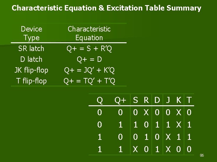
Characteristic Equation & Excitation Table Summary Device Type SR latch D latch JK flip-flop T flip-flop Characteristic Equation Q+ = S + R’Q Q+ = D Q+ = JQ’ + K’Q Q+ = TQ’ + T’Q Q 0 0 1 1 Q+ 0 1 S 0 1 0 X R X 0 1 0 D 0 1 J 0 1 X X K X X 1 0 T 0 1 1 0 86

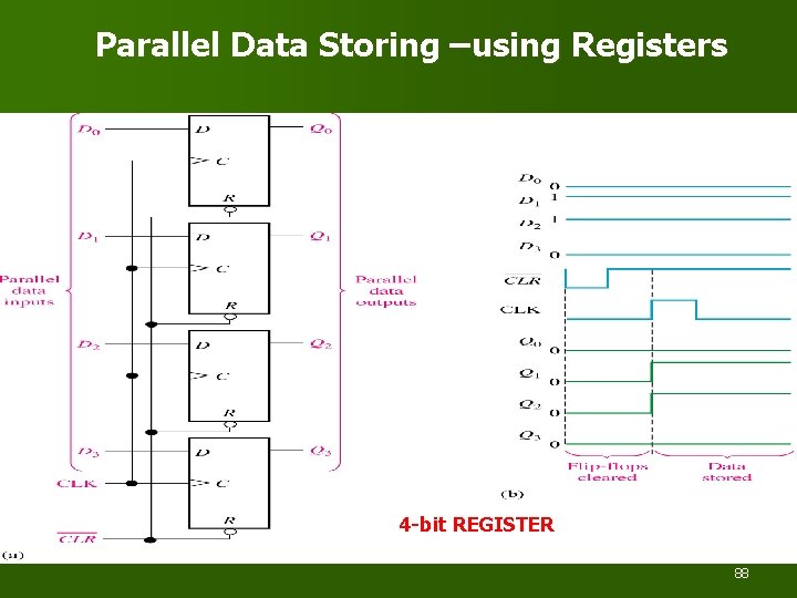
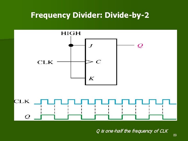
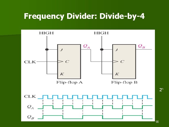
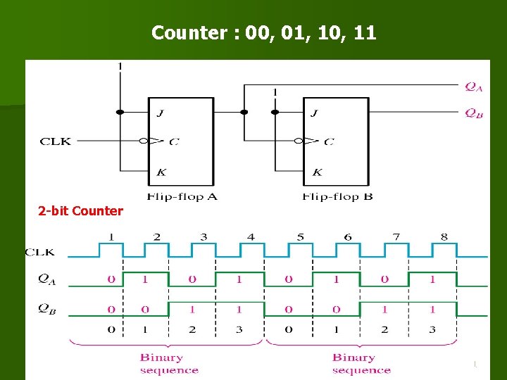
Flip-flop Applications Parallel Data Storing 2. Frequency Divider 3. Counter 1. 87

Parallel Data Storing –using Registers 4 -bit REGISTER 88

Frequency Divider: Divide-by-2 Q is one-half the frequency of CLK 89

Frequency Divider: Divide-by-4 2 n 90

Counter : 00, 01, 10, 11 2 -bit Counter 91

SEQUENTIAL CIRCUITS Design Examples Using Flip-flops 92

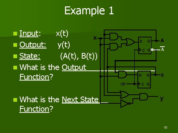
Example 1 n Input: x(t) x n Output: y(t) n State: (A(t), B(t)) n What is the Output Function? D CP n What is the Next State Function? Q A C Q A Q B D C Q y 93

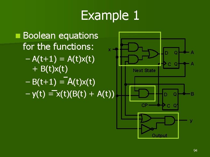
Example 1 n Boolean equations for the functions: x – A(t+1) = A(t)x(t) + B(t)x(t) Q A C Q A Q B D Next State – B(t+1) = A(t)x(t) – y(t) = x(t)(B(t) + A(t)) D CP C Q' y Output 94

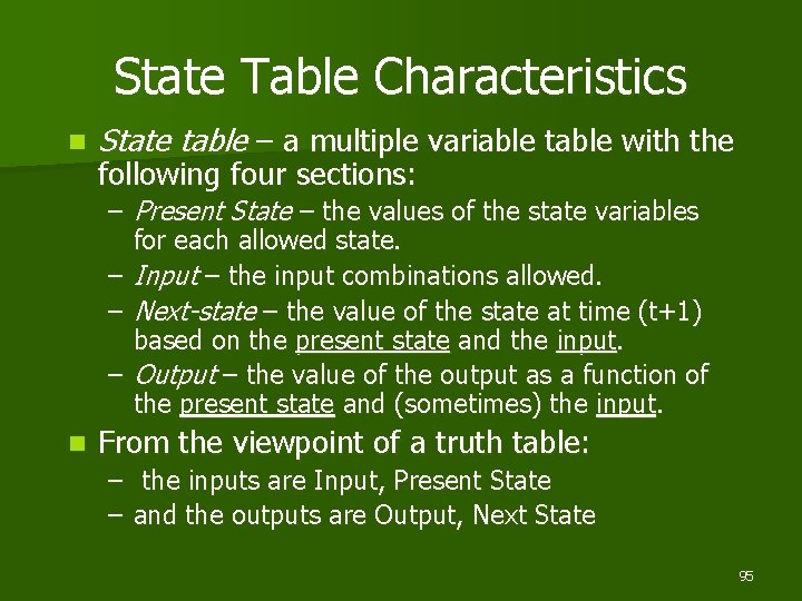
State Table Characteristics n State table – a multiple variable table with the following four sections: – Present State – the values of the state variables for each allowed state. – Input – the input combinations allowed. – Next-state – the value of the state at time (t+1) based on the present state and the input. – Output – the value of the output as a function of the present state and (sometimes) the input. n From the viewpoint of a truth table: – – the inputs are Input, Present State and the outputs are Output, Next State 95

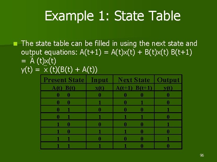
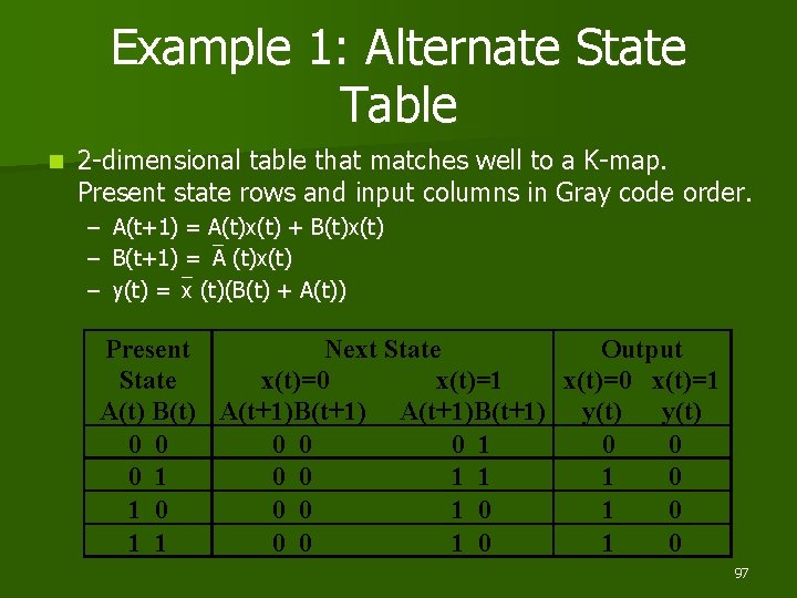
Example 1: State Table n The state table can be filled in using the next state and output equations: A(t+1) = A(t)x(t) + B(t)x(t) B(t+1) = A (t)x(t) y(t) = x (t)(B(t) + A(t)) Present State Input Next State Output A(t) 0 0 1 1 B(t) 0 0 1 1 x(t) 0 1 0 1 A(t+1) B(t+1) 0 0 0 1 1 0 0 0 1 0 y(t) 0 0 1 0 1 0 96

Example 1: Alternate State Table n 2 -dimensional table that matches well to a K-map. Present state rows and input columns in Gray code order. – – – A(t+1) = A(t)x(t) + B(t)x(t) B(t+1) = A (t)x(t) y(t) = x (t)(B(t) + A(t)) Present Next State Output State x(t)=0 x(t)=1 A(t) B(t) A(t+1)B(t+1) y(t) 0 0 0 1 1 1 0 0 0 1 0 1 1 0 0 1 0 97

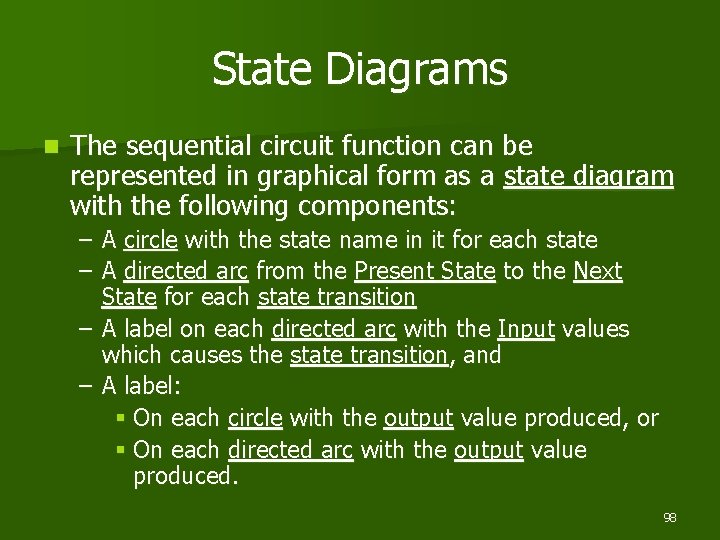
State Diagrams n The sequential circuit function can be represented in graphical form as a state diagram with the following components: – – A circle with the state name in it for each state A directed arc from the Present State to the Next State for each state transition – A label on each directed arc with the Input values which causes the state transition, and – A label: § On each circle with the output value produced, or § On each directed arc with the output value produced. 98

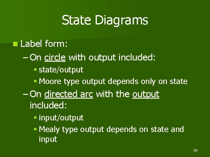
State Diagrams n Label form: – On circle with output included: § state/output § Moore type output depends only on state – On directed arc with the output included: § input/output § Mealy type output depends on state and input 99

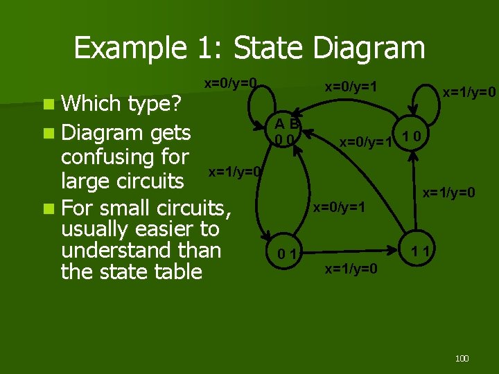
Example 1: State Diagram n Which x=0/y=0 type? n Diagram gets confusing for x=1/y=0 large circuits n For small circuits, usually easier to understand than the state table x=0/y=1 AB 00 x=0/y=1 1 0 x=0/y=1 01 x=1/y=0 11 x=1/y=0 100

Standard Graphic Symbols for Latch and Flip-Flops 101

102

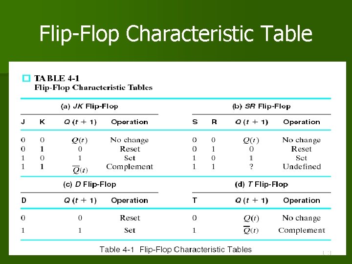
Flip-Flop Characteristic Table 103

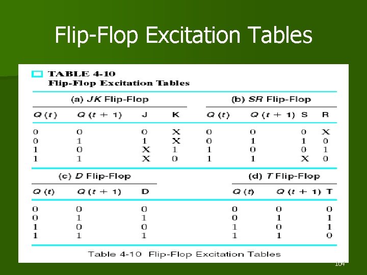
Flip-Flop Excitation Tables 104

Examples Using D-Flip-flop 105

Example 1 D-Flip-flop 106

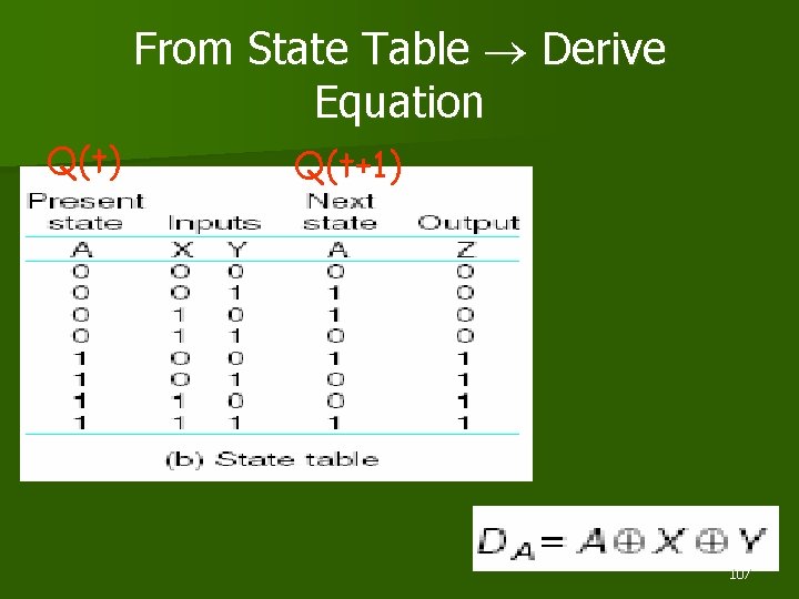
From State Table Derive Equation Q(t) Q(t+1) 107

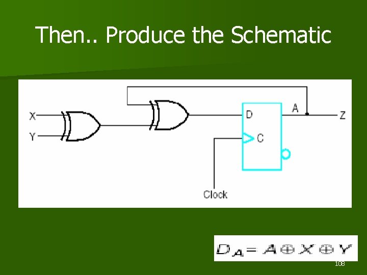
Then. . Produce the Schematic 108

Example 2 D-Flip-flop 109

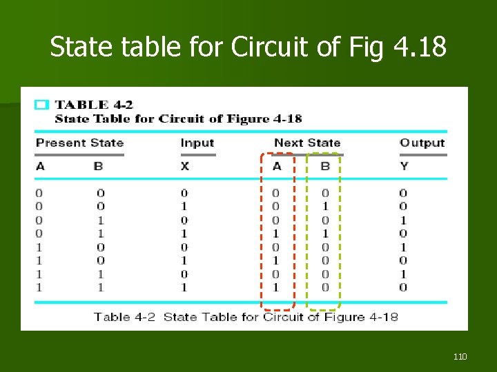
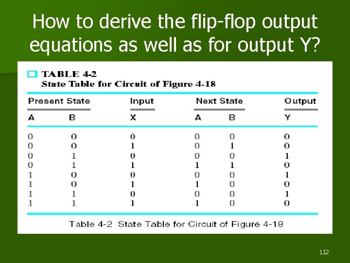
State table for Circuit of Fig 4. 18 110

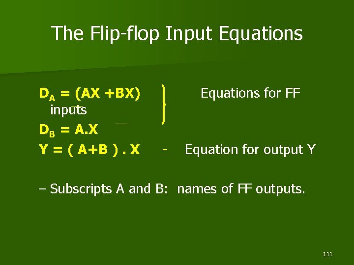
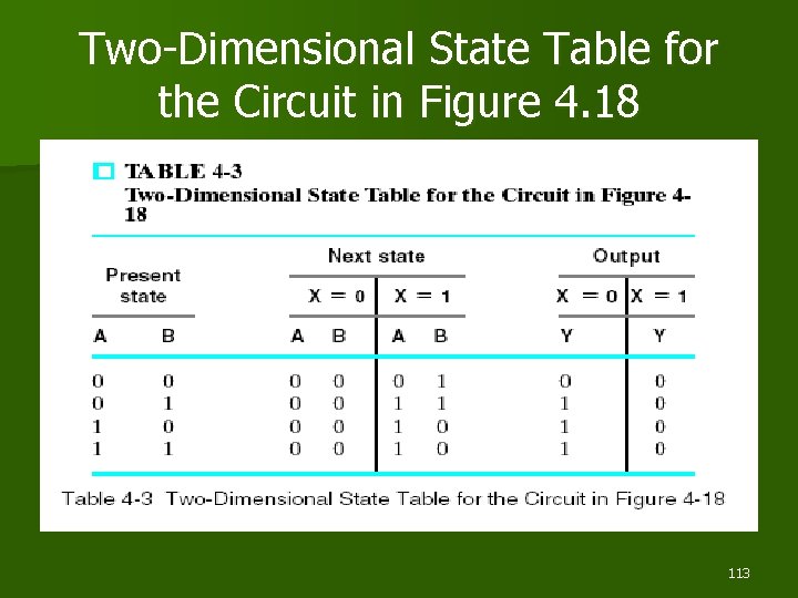
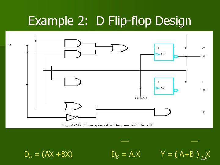
The Flip-flop Input Equations DA = (AX +BX) inputs DB = A. X Y = ( A+B ). X Equations for FF - Equation for output Y – Subscripts A and B: names of FF outputs. 111

How to derive the flip-flop output equations as well as for output Y? 112

Two-Dimensional State Table for the Circuit in Figure 4. 18 113

Example 2: D Flip-flop Design DA = (AX +BX) DB = A. X Y = ( A+B ) 114. X

Example 3 D-Flip-flop 115

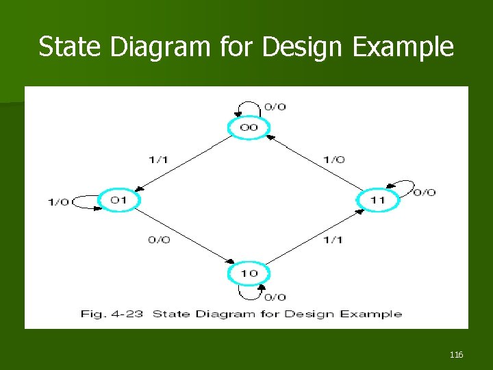
State Diagram for Design Example 116

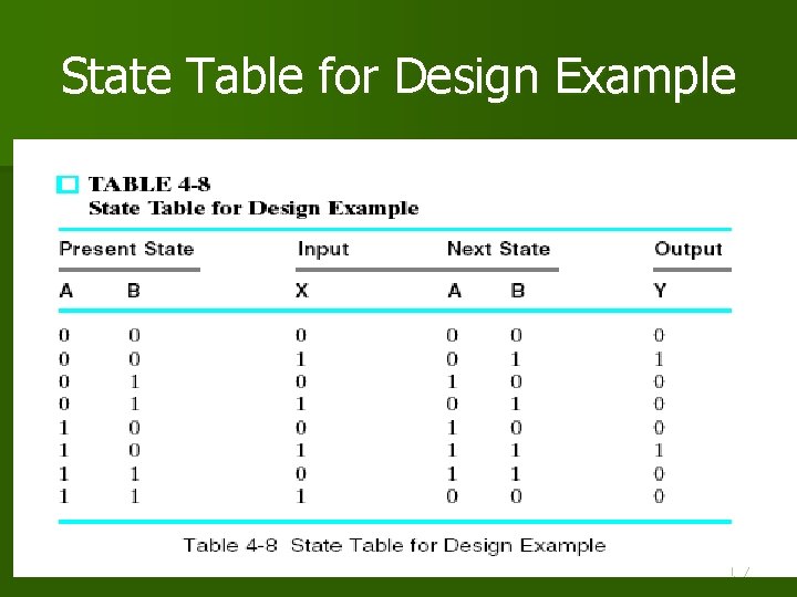
State Table for Design Example 117

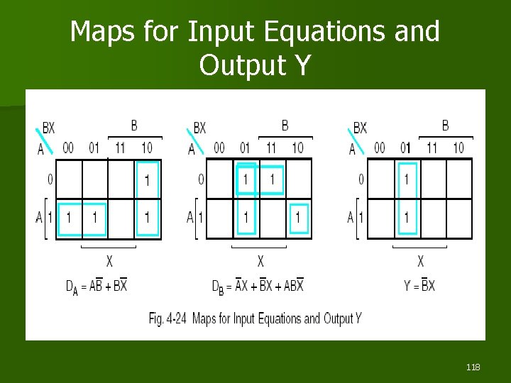
Maps for Input Equations and Output Y 118

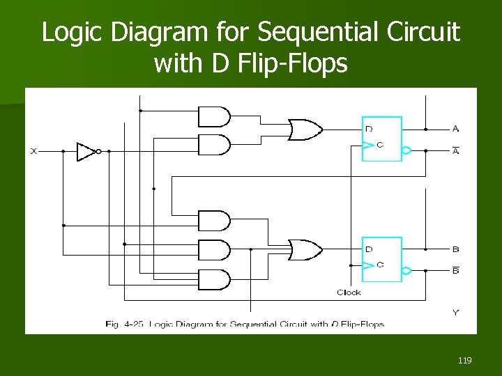
Logic Diagram for Sequential Circuit with D Flip-Flops 119

Example 4 D-Flip-flop 120

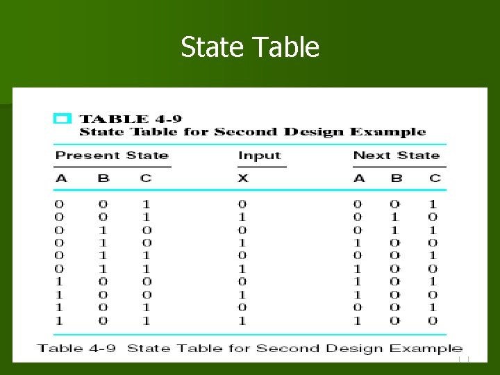
State Table 121

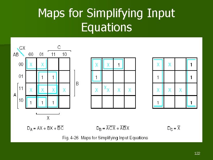
Maps for Simplifying Input Equations 122

The s. Che. Mati. C… 123