EKT 124 3 DIGITAL ELEKTRONIC 1 CHAPTER 3

- Slides: 60

EKT 124 / 3 DIGITAL ELEKTRONIC 1 CHAPTER 3 Counters

INTRODUCTION q One of the common requirement in digital circuits/system is counting, both direction (forward and backward) q Digital clocks and watches are everywhere, timers are found in a range of appliances from microwave ovens to VCRs, and counters for other reasons are found in everything from automobiles to test equipment. q Although we will see many variations on the basic counter, they are all fundamentally very similar.

INTRODUCTION (cont. ) q Counters can be implemented quite easily using register-type circuits such as the flip-flop, and a wide variety of classifications exist: § Asynchronous (ripple) counter – changing state bits are used as clocks § § § to subsequent state flip-flops Synchronous counter – all state bits change under control of a single clock Decade counter – counts through ten states per stage Up/down counter – counts both up and down, under command of a control input Ring counter – formed by a shift register with feedback connection in a ring Johnson counter – a twisted ring counter Cascaded counter q Each is useful for different applications

INTRODUCTION (cont. ) q A counter – a group of flip-flops connected together to perform counting operations. q The number of flip-flops used and the way in which they are connected determine the number of states (modulus). q Two broad categories according to the way they are clocked: § Asynchronous counter § Synchronous counter

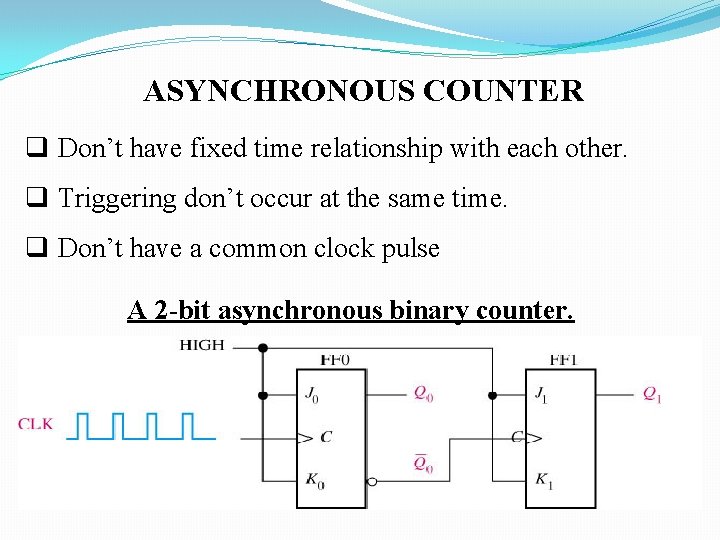
ASYNCHRONOUS COUNTER q Don’t have fixed time relationship with each other. q Triggering don’t occur at the same time. q Don’t have a common clock pulse A 2 -bit asynchronous binary counter.

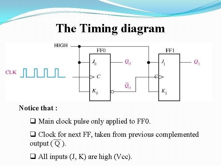
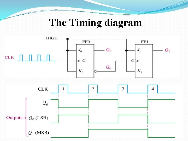
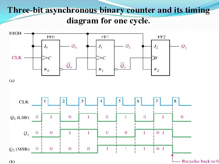
The Timing diagram Notice that : q Main clock pulse only applied to FF 0. q Clock for next FF, taken from previous complemented output ( Q ). q All inputs (J, K) are high (Vcc).

The Timing diagram

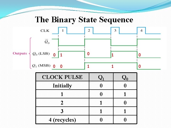
The Binary State Sequence 0 1 0 0 0 1 1 0 CLOCK PULSE Initially 1 2 Q 1 0 0 1 Q 0 0 1 0 3 4 (recycles) 1 0

Three-bit asynchronous binary counter and its timing diagram for one cycle.

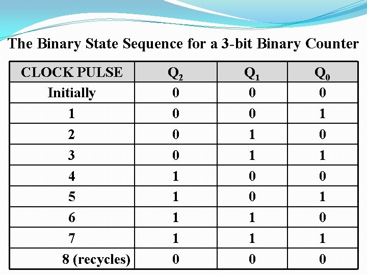
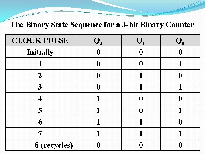
The Binary State Sequence for a 3 -bit Binary Counter CLOCK PULSE Initially 1 2 3 4 5 6 7 8 (recycles) Q 2 0 0 1 1 0 Q 1 0 0 1 1 0 Q 0 0 1 0 1 0

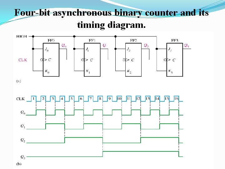
Four-bit asynchronous binary counter and its timing diagram.

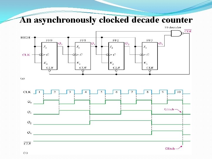
ASYNCHRONOUS DECADE COUNTER q The modulus of a counter is the number of unique states that the counter will sequence through. q The maximum possible number of states (max modulus) is 2 n where n is the number of flip-flops. q Counter with ten states are called decade counter. q Counter can also be designed to have a number of states in their sequence that is less than the maximum of 2 n. The resulting sequence is called truncated sequence. q To obtain a truncated sequence it is necessary to force the counter to recycle before going through all of its possible states.

An asynchronously clocked decade counter

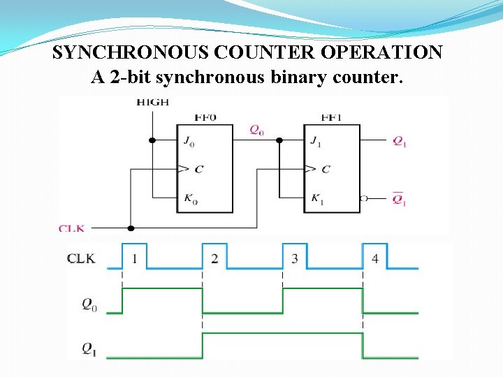
SYNCHRONOUS COUNTER OPERATION A 2 -bit synchronous binary counter.

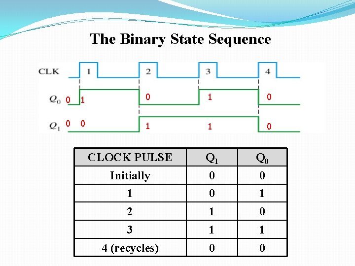
The Binary State Sequence 0 1 0 0 0 1 1 0 CLOCK PULSE Q 1 Q 0 Initially 0 0 1 2 1 0 3 1 1 4 (recycles) 0 0

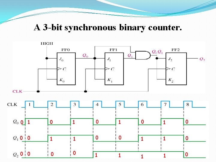
A 3 -bit synchronous binary counter. 0 1 0 1 0 0 0 1 1 0

The Binary State Sequence for a 3 -bit Binary Counter CLOCK PULSE Initially 1 2 3 4 5 6 7 8 (recycles) Q 2 0 0 1 1 0 Q 1 0 0 1 1 0 Q 0 0 1 0 1 0

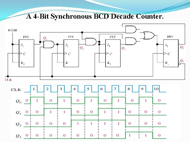
A 4 -Bit Synchronous BCD Decade Counter.

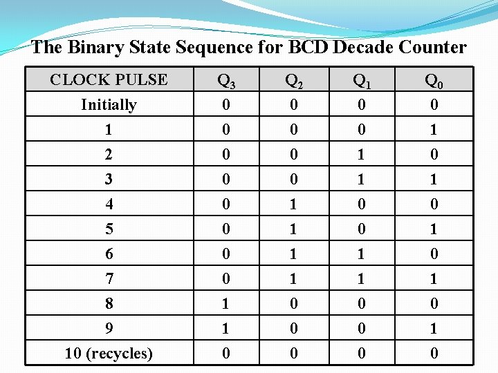
The Binary State Sequence for BCD Decade Counter CLOCK PULSE Initially 1 2 Q 3 0 0 0 Q 2 0 0 0 Q 1 0 0 1 Q 0 0 1 0 3 4 5 6 7 8 9 10 (recycles) 0 0 0 1 1 0 0 0 1 1 0 0 0 1 0 1 0

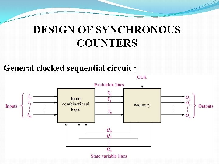
DESIGN OF SYNCHRONOUS COUNTERS General clocked sequential circuit :

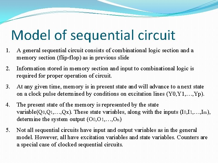
Model of sequential circuit 1. A general sequential circuit consists of combinational logic section and a memory section (flip-flop) as in previous slide 2. Information stored in memory section and input to combinational logic is required for properation of circuit. 3. At any given time, memory is in present state and will advance to a next state on a clock pulse determined by conditions on excitation lines (Y 0, Y 1, …, Yp). 4. The present state of the memory is represented by the state variable(Q 0, Q 1, …, Qx). These state variables, along with the inputs (I 0, I 1, …, Im), determine the system output (O 0, O 1, …, On) 5. Not all sequential circuits have input and output variables as in the general model. However, all have excitation variables and state variables. Counters are a special case of clocked sequential circuits.

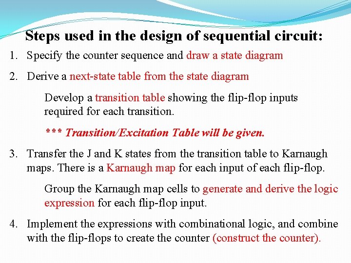
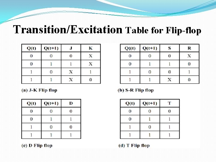
Steps used in the design of sequential circuit: 1. Specify the counter sequence and draw a state diagram 2. Derive a next-state table from the state diagram Develop a transition table showing the flip-flop inputs required for each transition. *** Transition/Excitation Table will be given. 3. Transfer the J and K states from the transition table to Karnaugh maps. There is a Karnaugh map for each input of each flip-flop. Group the Karnaugh map cells to generate and derive the logic expression for each flip-flop input. 4. Implement the expressions with combinational logic, and combine with the flip-flops to create the counter (construct the counter).

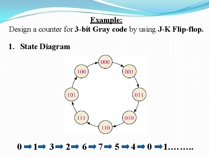
Example: Design a counter for 3 -bit Gray code by using J-K Flip-flop. 1. State Diagram 0 1 3 2 6 7 5 4 0 1. ……. .

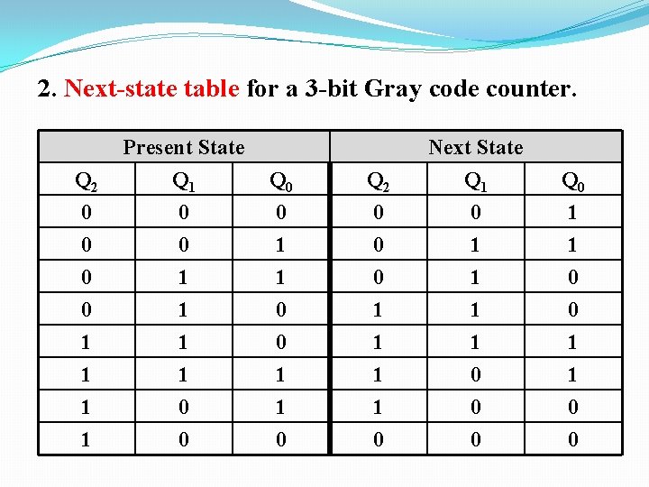
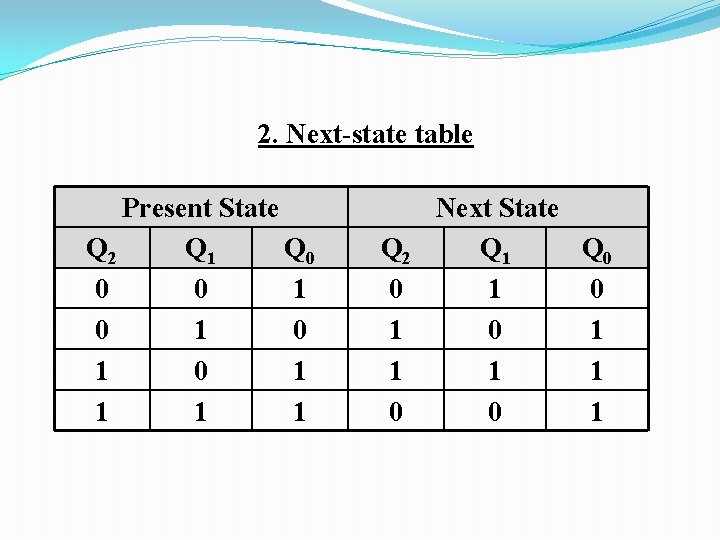
2. Next-state table for a 3 -bit Gray code counter. Q 2 0 0 Present State Q 1 0 0 Q 0 0 1 1 1 1 1 0 0 1 1 0 Q 2 0 0 Next State Q 1 0 1 Q 0 1 1 1 1 0 0 0 1 1 0 0

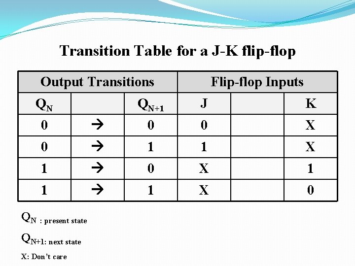
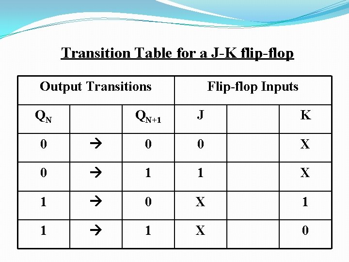
Transition Table for a J-K flip-flop Output Transitions QN QN Flip-flop Inputs QN+1 J K 0 0 0 X 0 1 1 X 1 0 X 1 1 1 X 0 : present state QN+1: next state X: Don’t care

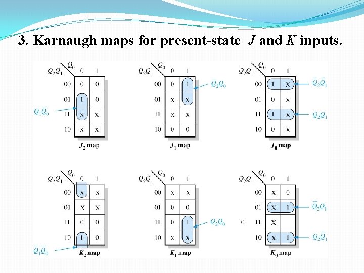
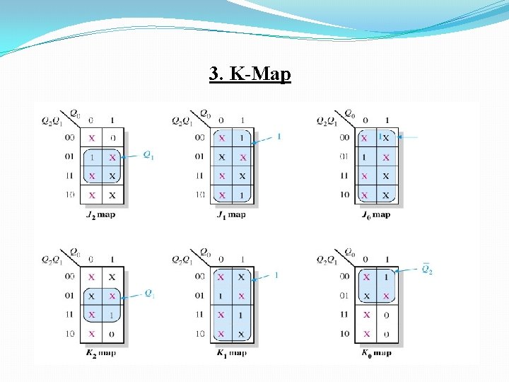
3. Karnaugh maps for present-state J and K inputs.

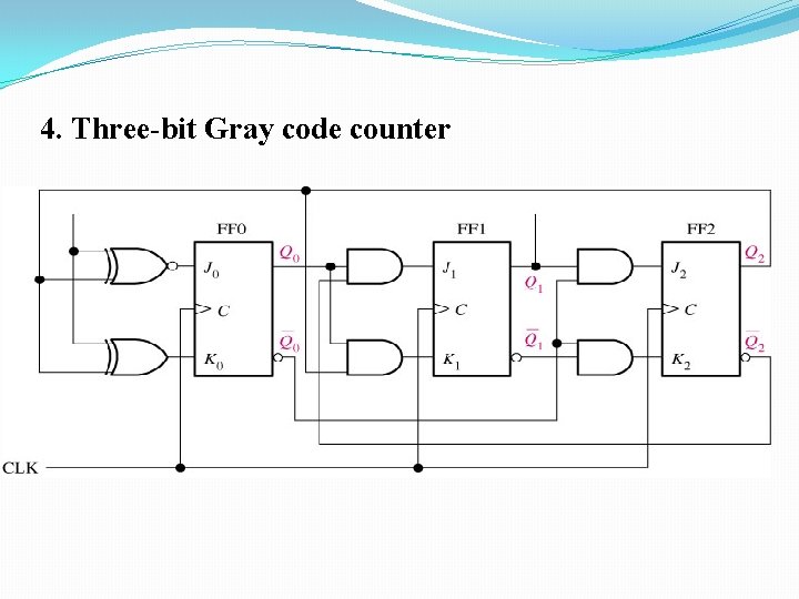
4. Three-bit Gray code counter

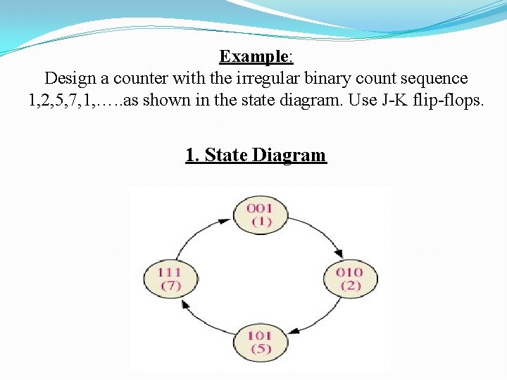
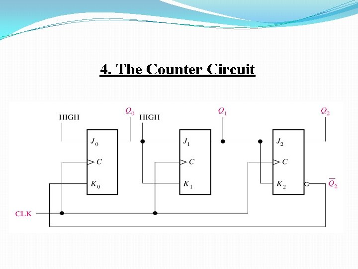
Example: Design a counter with the irregular binary count sequence 1, 2, 5, 7, 1, …. . as shown in the state diagram. Use J-K flip-flops. 1. State Diagram

2. Next-state table Present State Q 2 Q 1 Q 0 0 0 1 0 1 1 1 1 Q 2 0 1 1 0 Next State Q 1 Q 0 1 0 0 1 1 1 0 1

Transition Table for a J-K flip-flop Output Transitions QN Flip-flop Inputs QN+1 J K 0 0 0 X 0 1 1 X 1 0 X 1 1 1 X 0

3. K-Map

4. The Counter Circuit

Transition/Excitation Table for Flip-flop

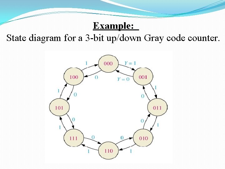
Example: State diagram for a 3 -bit up/down Gray code counter.

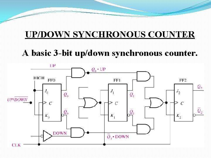
UP/DOWN SYNCHRONOUS COUNTER A basic 3 -bit up/down synchronous counter.

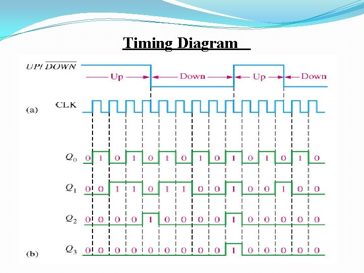
Timing Diagram

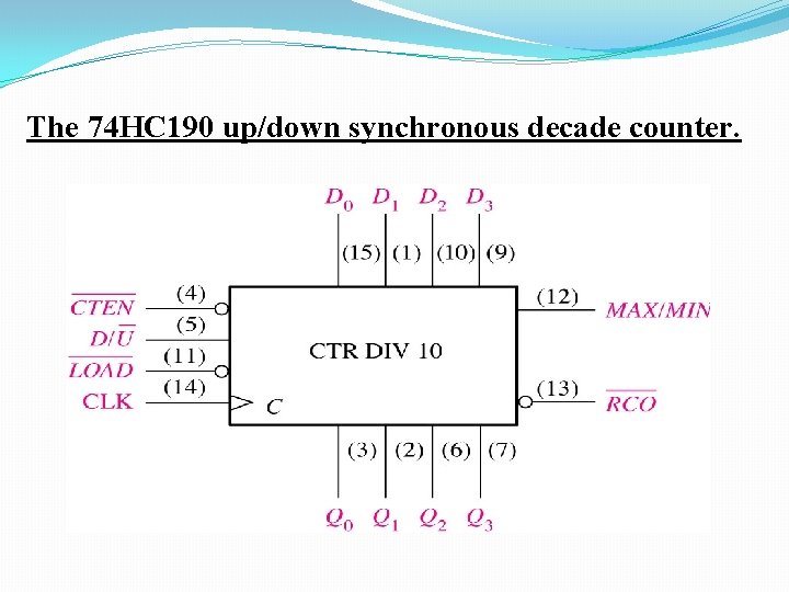
The 74 HC 190 up/down synchronous decade counter.

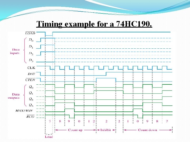
Timing example for a 74 HC 190.

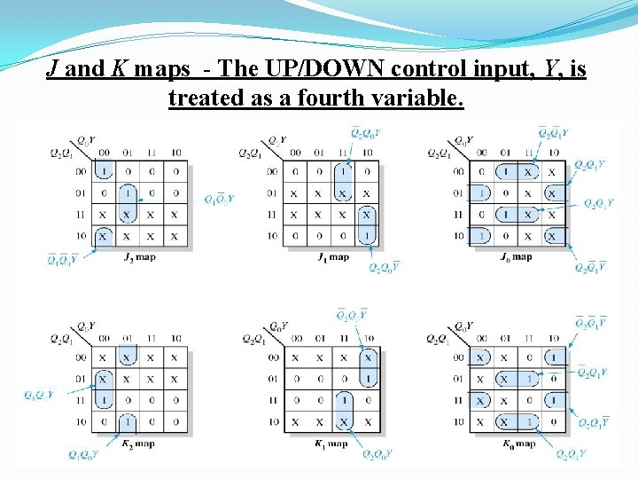
J and K maps - The UP/DOWN control input, Y, is treated as a fourth variable.

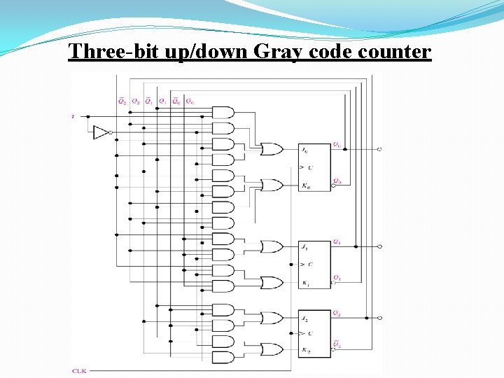
Three-bit up/down Gray code counter

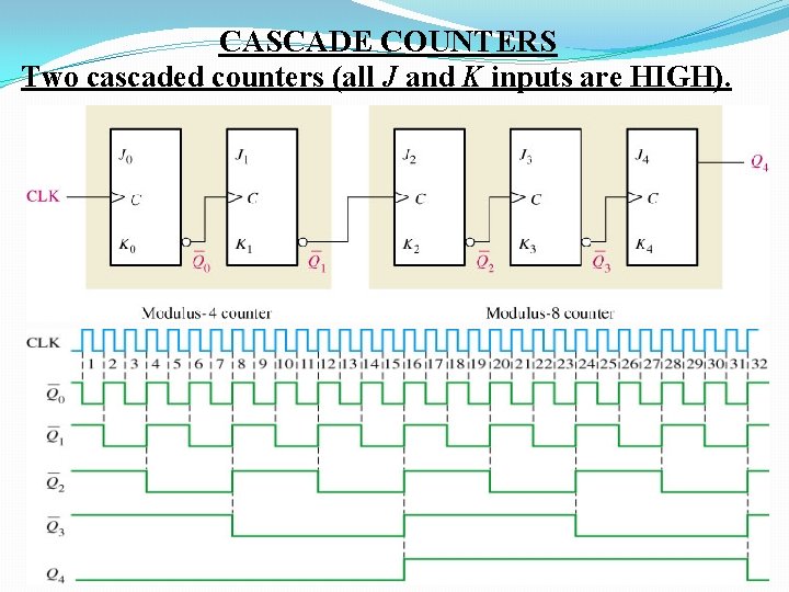
CASCADE COUNTERS Two cascaded counters (all J and K inputs are HIGH).

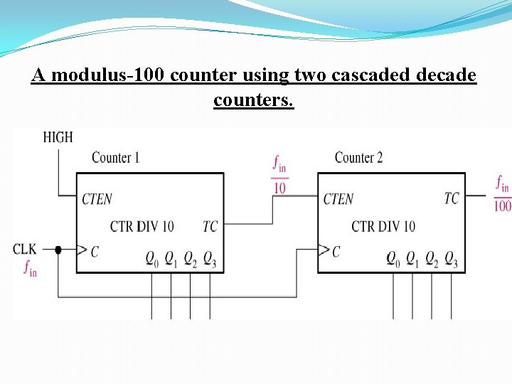
A modulus-100 counter using two cascaded decade counters.

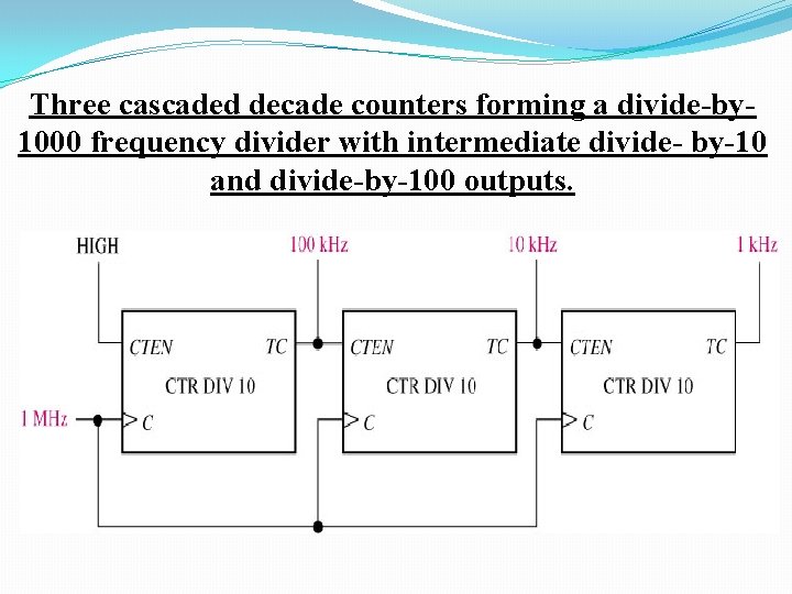
Three cascaded decade counters forming a divide-by 1000 frequency divider with intermediate divide- by-10 and divide-by-100 outputs.

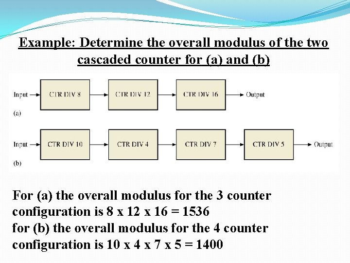
Example: Determine the overall modulus of the two cascaded counter for (a) and (b) For (a) the overall modulus for the 3 counter configuration is 8 x 12 x 16 = 1536 for (b) the overall modulus for the 4 counter configuration is 10 x 4 x 7 x 5 = 1400

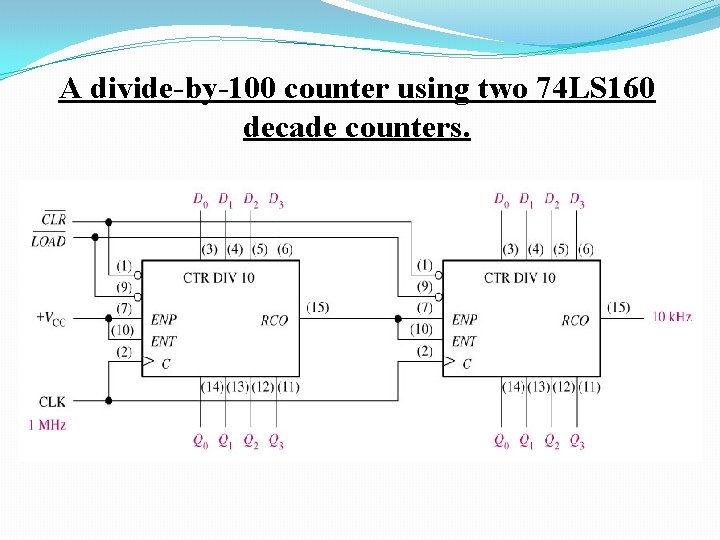
A divide-by-100 counter using two 74 LS 160 decade counters.

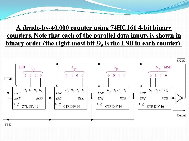
A divide-by-40, 000 counter using 74 HC 161 4 -bit binary counters. Note that each of the parallel data inputs is shown in binary order (the right-most bit D 0 is the LSB in each counter).

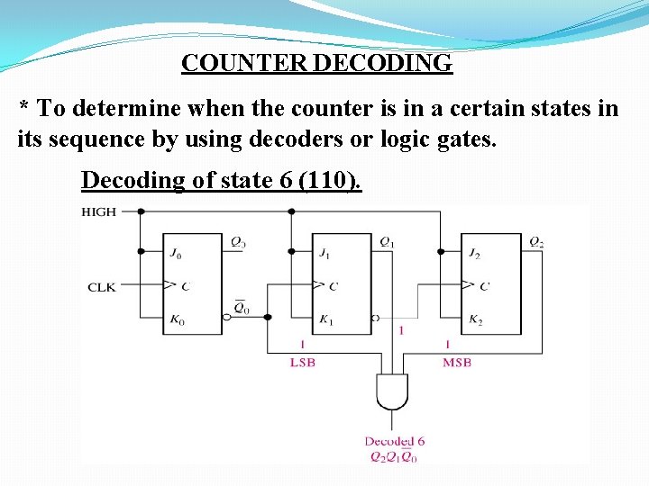
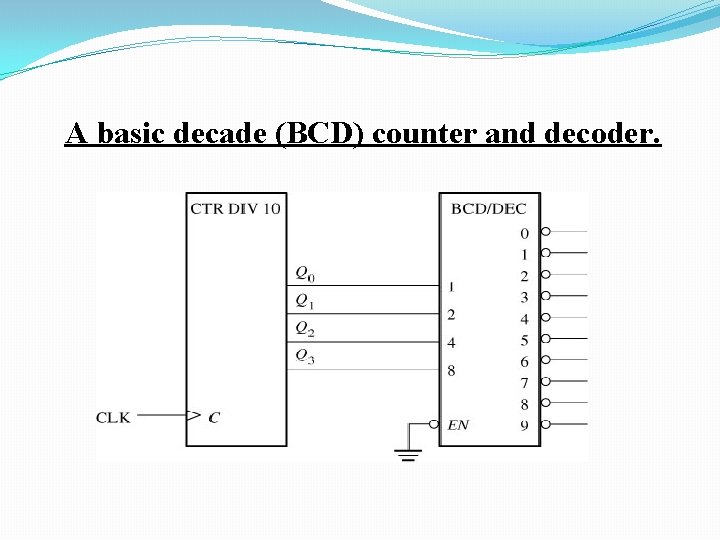
COUNTER DECODING * To determine when the counter is in a certain states in its sequence by using decoders or logic gates. Decoding of state 6 (110).

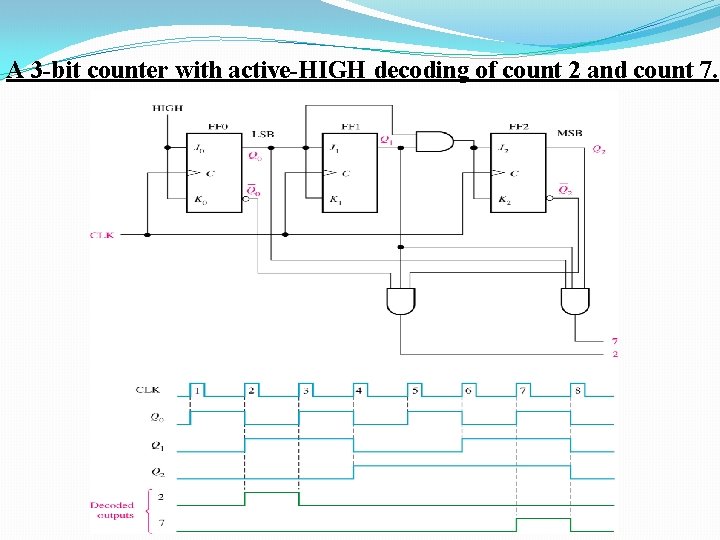
A 3 -bit counter with active-HIGH decoding of count 2 and count 7.

A basic decade (BCD) counter and decoder.

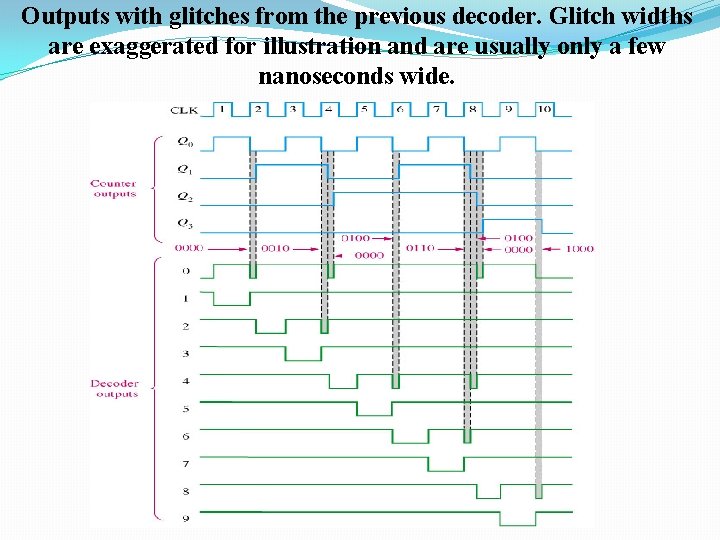
Outputs with glitches from the previous decoder. Glitch widths are exaggerated for illustration and are usually only a few nanoseconds wide.

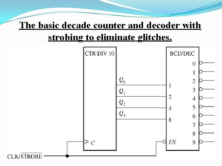
The basic decade counter and decoder with strobing to eliminate glitches.

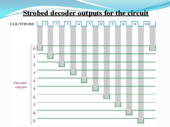
Strobed decoder outputs for the circuit

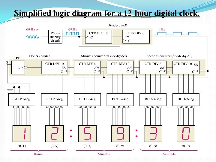
Simplified logic diagram for a 12 -hour digital clock.

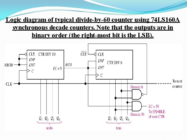
Logic diagram of typical divide-by-60 counter using 74 LS 160 A synchronous decade counters. Note that the outputs are in binary order (the right-most bit is the LSB).

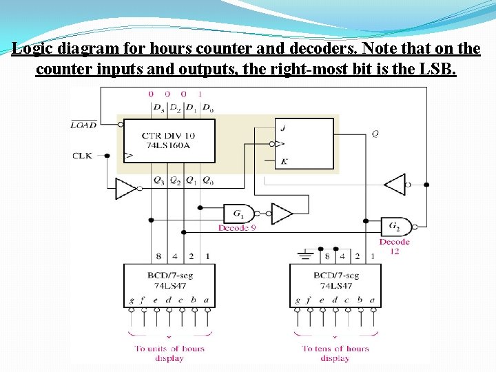
Logic diagram for hours counter and decoders. Note that on the counter inputs and outputs, the right-most bit is the LSB.

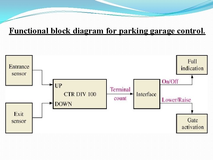
Functional block diagram for parking garage control.

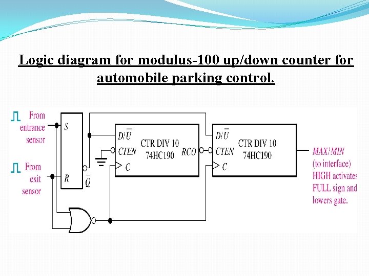
Logic diagram for modulus-100 up/down counter for automobile parking control.

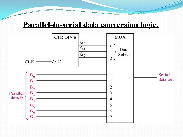
Parallel-to-serial data conversion logic.

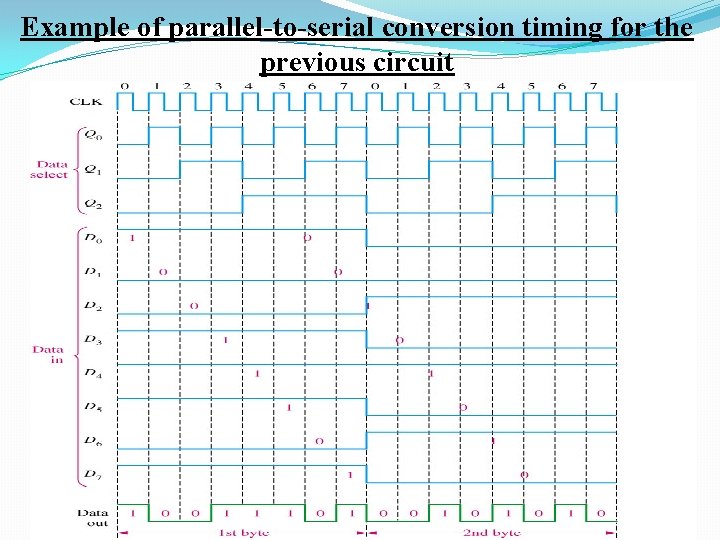
Example of parallel-to-serial conversion timing for the previous circuit

THANK YOU