Chapter 6 Diode Transistor Logic DTL Digital Electronics
- Slides: 27

Chapter 6 Diode Transistor Logic – DTL Digital Electronics ELE 450 A First 2015/2016 Dr. Idrees Al-Kofahi 1

Diode Transistor Logic • One of the major issues with RTL is its low fanout. – Even with adding active devices to the output, the fan-out is still quite limited. • In the early 1960's, a solution for the problem was proposed in the form of a new logic family which utilizes diodes in addition to transistors. Digital Electronics ELE 450 A First 2015/2016 Dr. Idrees Al-Kofahi 2

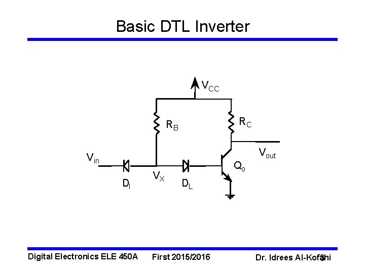
Basic DTL Inverter VCC RC RB Vout Vin DI Digital Electronics ELE 450 A VX Qo DL First 2015/2016 Dr. Idrees Al-Kofahi 3

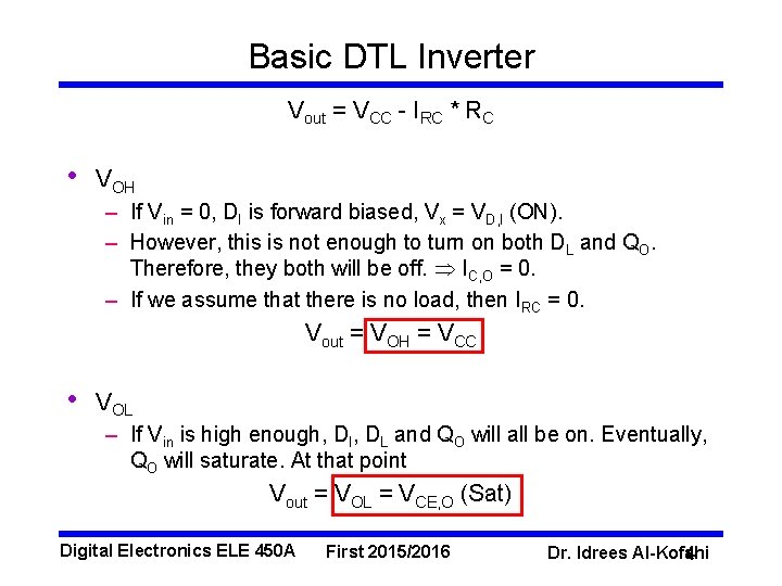
Basic DTL Inverter Vout = VCC - IRC * RC • VOH – If Vin = 0, DI is forward biased, Vx = VD, I (ON). – However, this is not enough to turn on both DL and QO. Therefore, they both will be off. IC, O = 0. – If we assume that there is no load, then IRC = 0. Vout = VOH = VCC • VOL – If Vin is high enough, DI, DL and QO will all be on. Eventually, QO will saturate. At that point Vout = VOL = VCE, O (Sat) Digital Electronics ELE 450 A First 2015/2016 Dr. Idrees Al-Kofahi 4

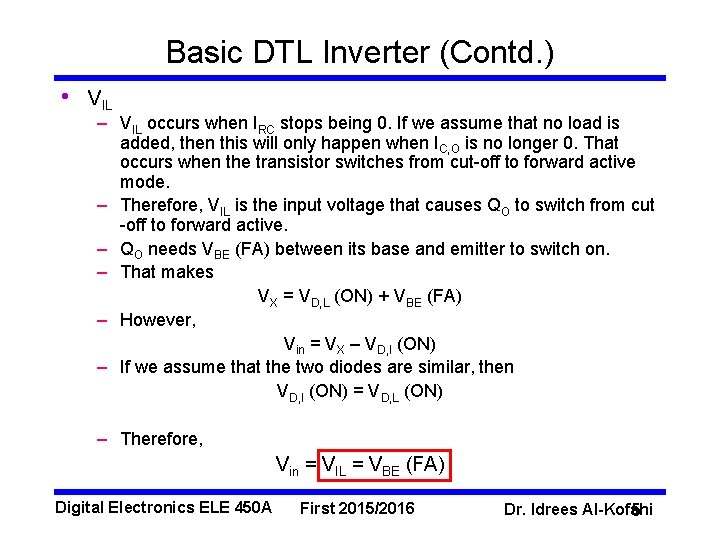
Basic DTL Inverter (Contd. ) • VIL – VIL occurs when IRC stops being 0. If we assume that no load is added, then this will only happen when IC, O is no longer 0. That occurs when the transistor switches from cut-off to forward active mode. – Therefore, VIL is the input voltage that causes QO to switch from cut -off to forward active. – QO needs VBE (FA) between its base and emitter to switch on. – That makes VX = VD, L (ON) + VBE (FA) – However, Vin = VX – VD, I (ON) – If we assume that the two diodes are similar, then VD, I (ON) = VD, L (ON) – Therefore, Vin = VIL = VBE (FA) Digital Electronics ELE 450 A First 2015/2016 Dr. Idrees Al-Kofahi 5

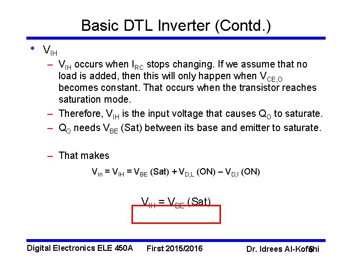
Basic DTL Inverter (Contd. ) • VIH – VIH occurs when IRC stops changing. If we assume that no load is added, then this will only happen when VCE, O becomes constant. That occurs when the transistor reaches saturation mode. – Therefore, VIH is the input voltage that causes QO to saturate. – QO needs VBE (Sat) between its base and emitter to saturate. – That makes Vin = VIH = VBE (Sat) + VD, L (ON) – VD, I (ON) VIH = VBE (Sat) Digital Electronics ELE 450 A First 2015/2016 Dr. Idrees Al-Kofahi 6

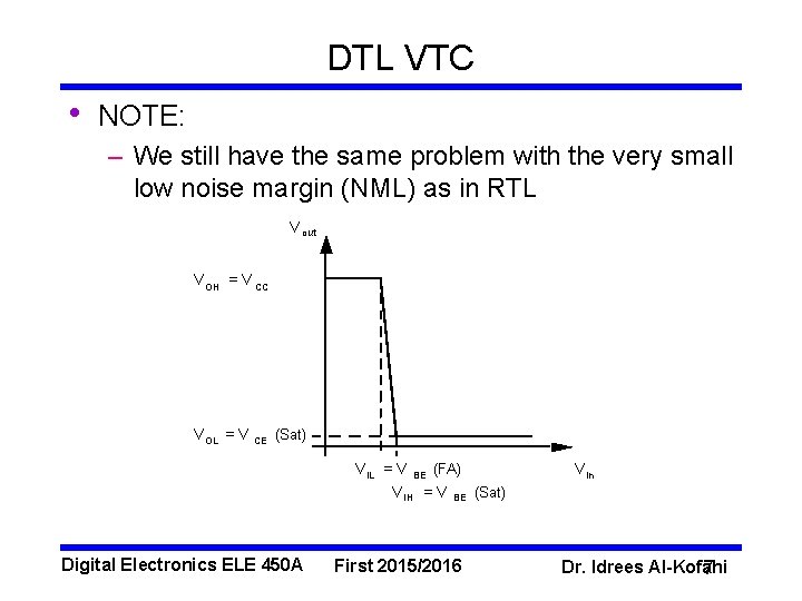
DTL VTC • NOTE: – We still have the same problem with the very small low noise margin (NML) as in RTL V out V OH = V CC V OL = V CE (Sat) V IL = V BE (FA) V IH = V Digital Electronics ELE 450 A BE First 2015/2016 V in (Sat) Dr. Idrees Al-Kofahi 7

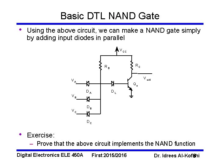
Basic DTL NAND Gate • Using the above circuit, we can make a NAND gate simply by adding input diodes in parallel V CC RC RB V out VA VB VC Qo DA DL DB DC • Exercise: – Prove that the above circuit implements the NAND function Digital Electronics ELE 450 A First 2015/2016 Dr. Idrees Al-Kofahi 8

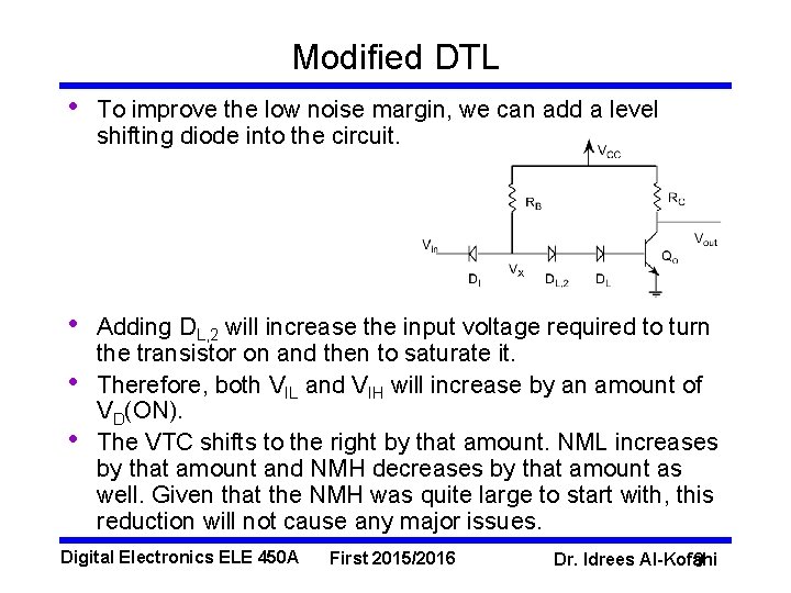
Modified DTL • To improve the low noise margin, we can add a level shifting diode into the circuit. • Adding DL, 2 will increase the input voltage required to turn the transistor on and then to saturate it. Therefore, both VIL and VIH will increase by an amount of VD(ON). The VTC shifts to the right by that amount. NML increases by that amount and NMH decreases by that amount as well. Given that the NMH was quite large to start with, this reduction will not cause any major issues. • • Digital Electronics ELE 450 A First 2015/2016 Dr. Idrees Al-Kofahi 9

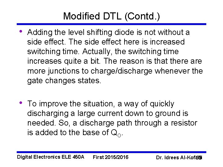
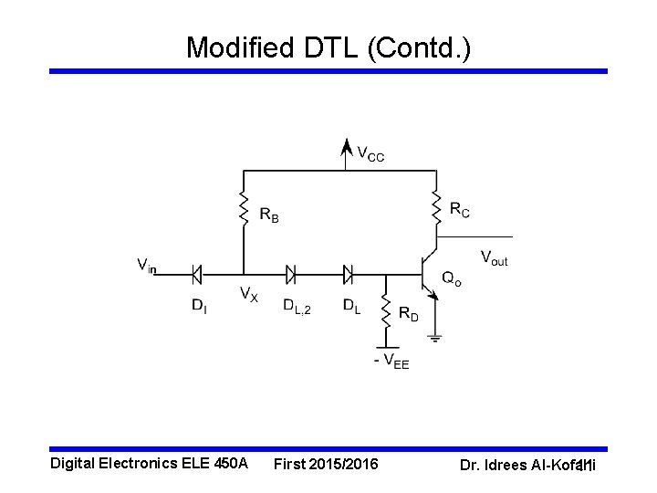
Modified DTL (Contd. ) • Adding the level shifting diode is not without a side effect. The side effect here is increased switching time. Actually, the switching time increases quite a bit. The reason is that there are more junctions to charge/discharge whenever the gate changes states. • To improve the situation, a way of quickly discharging a large current down to ground is needed. So, a discharge path through a resistor is added to the base of QO. Digital Electronics ELE 450 A First 2015/2016 Dr. Idrees Al-Kofahi 10

Modified DTL (Contd. ) Digital Electronics ELE 450 A First 2015/2016 Dr. Idrees Al-Kofahi 11

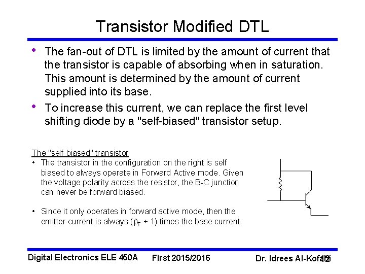
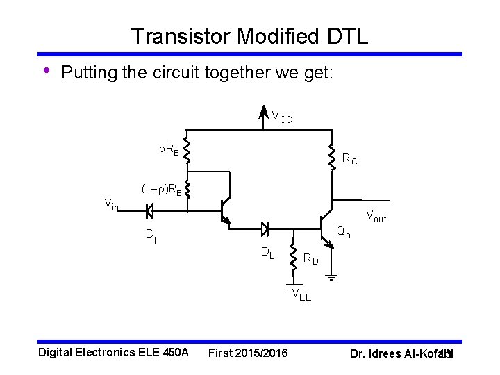
Transistor Modified DTL • • The fan-out of DTL is limited by the amount of current that the transistor is capable of absorbing when in saturation. This amount is determined by the amount of current supplied into its base. To increase this current, we can replace the first level shifting diode by a "self-biased" transistor setup. The "self-biased" transistor • The transistor in the configuration on the right is self biased to always operate in Forward Active mode. Given the voltage polarity across the resistor, the B-C junction can never be forward biased. • Since it only operates in forward active mode, then the emitter current is always (b. F + 1) times the base current. Digital Electronics ELE 450 A First 2015/2016 Dr. Idrees Al-Kofahi 12

Transistor Modified DTL • Putting the circuit together we get: VCC r. RB Vin RC (1 -r)RB Vout DI Qo DL RD - VEE Digital Electronics ELE 450 A First 2015/2016 Dr. Idrees Al-Kofahi 13

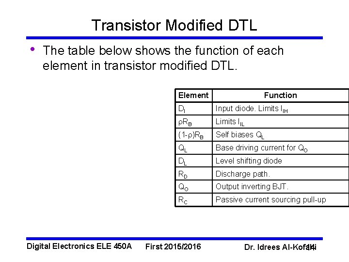
Transistor Modified DTL • The table below shows the function of each element in transistor modified DTL. Element Digital Electronics ELE 450 A Function DI Input diode. Limits IIH r. RB Limits IIL (1 -r)RB Self biases QL QL Base driving current for QO DL Level shifting diode RD Discharge path. QO Output inverting BJT. RC Passive current sourcing pull-up First 2015/2016 Dr. Idrees Al-Kofahi 14

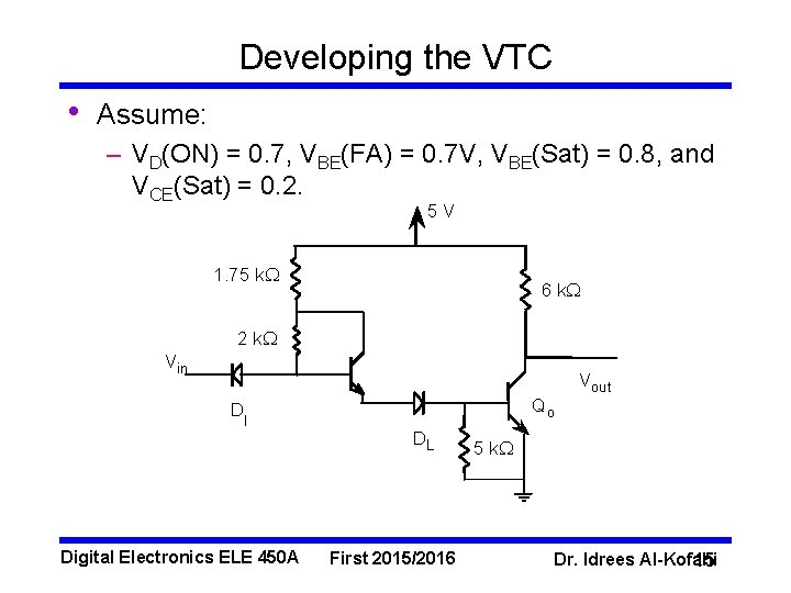
Developing the VTC • Assume: – VD(ON) = 0. 7, VBE(FA) = 0. 7 V, VBE(Sat) = 0. 8, and VCE(Sat) = 0. 2. 5 V 1. 75 k. W 6 k. W 2 k. W Vin Vout DI Digital Electronics ELE 450 A Qo DL First 2015/2016 5 k. W Dr. Idrees Al-Kofahi 15

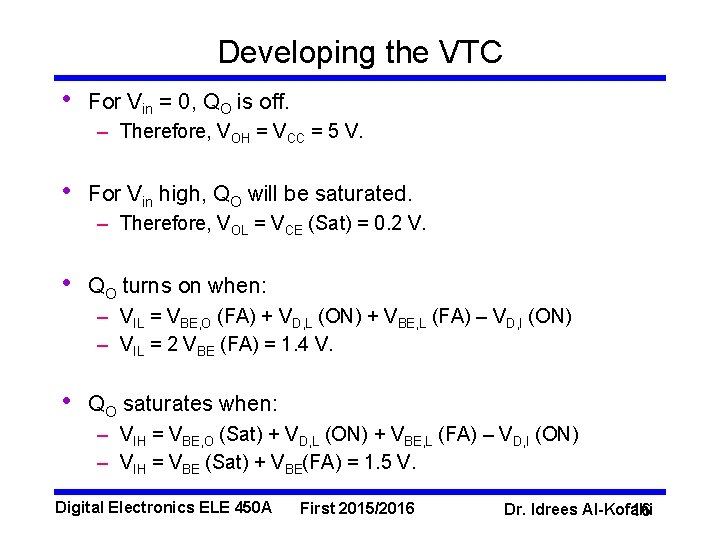
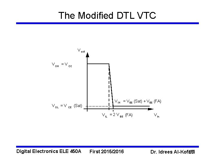
Developing the VTC • For Vin = 0, QO is off. – Therefore, VOH = VCC = 5 V. • For Vin high, QO will be saturated. – Therefore, VOL = VCE (Sat) = 0. 2 V. • QO turns on when: – VIL = VBE, O (FA) + VD, L (ON) + VBE, L (FA) – VD, I (ON) – VIL = 2 VBE (FA) = 1. 4 V. • QO saturates when: – VIH = VBE, O (Sat) + VD, L (ON) + VBE, L (FA) – VD, I (ON) – VIH = VBE (Sat) + VBE(FA) = 1. 5 V. Digital Electronics ELE 450 A First 2015/2016 Dr. Idrees Al-Kofahi 16

The Modified DTL VTC V out V OH = V CC V OL = V CE (Sat) V IH = VBE (Sat) + VBE (FA) V IL = 2 V BE (FA) Digital Electronics ELE 450 A First 2015/2016 V in Dr. Idrees Al-Kofahi 17

The Modified DTL Fan-out • Output high fan-out. – When the output of the driving gate is high, the input diodes of all load gates will be turned off. – Therefore, IIH = 0. – Output high fan-out is infinite. • Output low fan-out. – The maximum fan-out can be determined by how much output current – IOL – the driving gate can sink into the collector of QO compared to the amount of current generated from the input of each load gate – IIL. Digital Electronics ELE 450 A First 2015/2016 Dr. Idrees Al-Kofahi 18

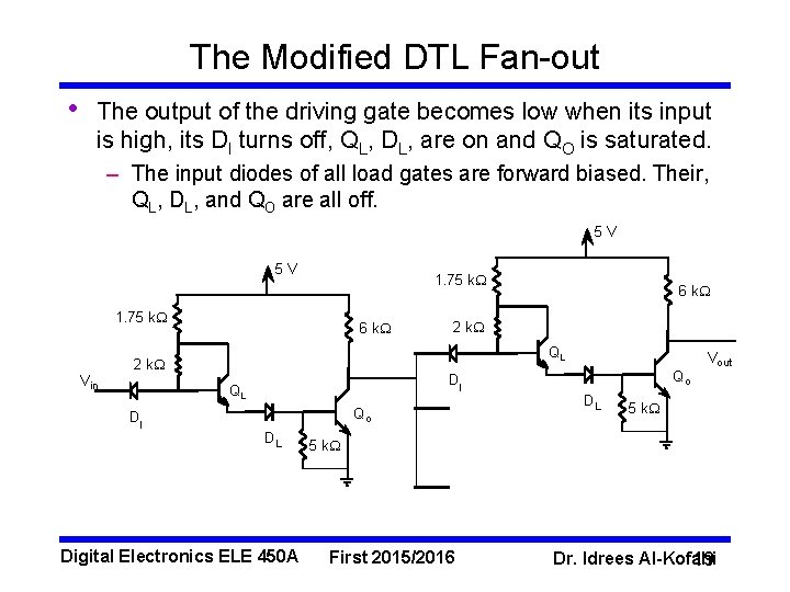
The Modified DTL Fan-out • The output of the driving gate becomes low when its input is high, its DI turns off, QL, DL, are on and QO is saturated. – The input diodes of all load gates are forward biased. Their, QL, DL, and QO are all off. 5 V 5 V 1. 75 k. W 6 k. W DI QL DI 2 k. W QL 2 k. W Vin 6 k. W Qo DL Digital Electronics ELE 450 A Qo DL Vout 5 k. W First 2015/2016 Dr. Idrees Al-Kofahi 19

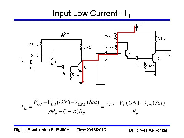
Input Low Current - IIL 5 V 5 V 1. 75 k. W 6 k. W DI QL DI 2 k. W QL 2 k. W Vin 6 k. W Qo DL Digital Electronics ELE 450 A Qo DL Vout 5 k. W First 2015/2016 Dr. Idrees Al-Kofahi 20

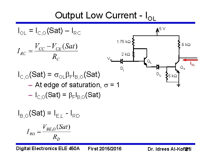
Output Low Current - IOL = IC, O(Sat) – IRC 5 V 1. 75 k. W 6 k. W 2 k. W Vin IC, O(Sat) = s. OLb. FIB, O(Sat) QL DI Qo DL IOL 5 k. W – At edge of saturation, s = 1 – IC, O(Sat) = b. FIB, O(Sat) = IE, L - IRD Digital Electronics ELE 450 A First 2015/2016 Dr. Idrees Al-Kofahi 21

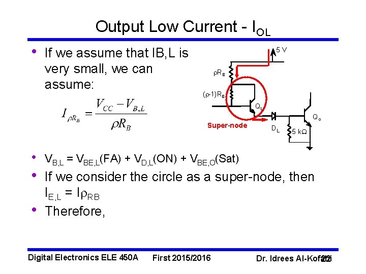
Output Low Current - IOL • If we assume that IB, L is very small, we can assume: 5 V r. RB (r-1)RB QL Super-node Qo DL 5 k. W • VB, L = VBE, L(FA) + VD, L(ON) + VBE, O(Sat) • If we consider the circle as a super-node, then IE, L = Ir. RB Therefore, • Digital Electronics ELE 450 A First 2015/2016 Dr. Idrees Al-Kofahi 22

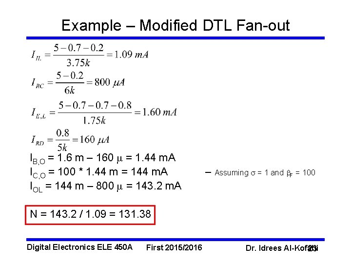
Example – Modified DTL Fan-out IB, O = 1. 6 m – 160 m = 1. 44 m. A IC, O = 100 * 1. 44 m = 144 m. A IOL = 144 m – 800 m = 143. 2 m. A – Assuming s = 1 and b. F = 100 N = 143. 2 / 1. 09 = 131. 38 Digital Electronics ELE 450 A First 2015/2016 Dr. Idrees Al-Kofahi 23

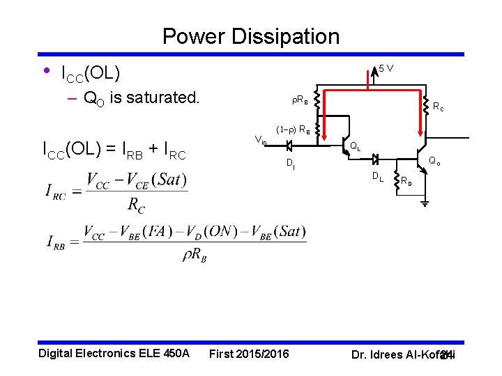
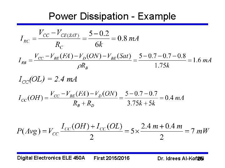
Power Dissipation • ICC(OL) 5 V – QO is saturated. ICC(OL) = IRB + IRC Digital Electronics ELE 450 A r. RB Vin RC (1 -r) RB QL DI First 2015/2016 Qo DL RD Dr. Idrees Al-Kofahi 24

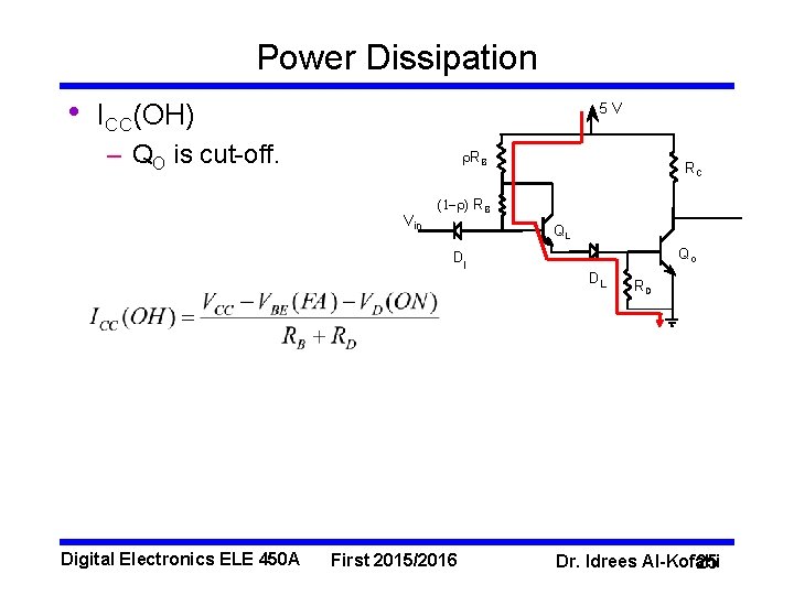
Power Dissipation • ICC(OH) 5 V – QO is cut-off. r. RB Vin (1 -r) RB QL DI Digital Electronics ELE 450 A RC First 2015/2016 Qo DL RD Dr. Idrees Al-Kofahi 25

Power Dissipation - Example ICC(OL) = 2. 4 m. A Digital Electronics ELE 450 A First 2015/2016 Dr. Idrees Al-Kofahi 26

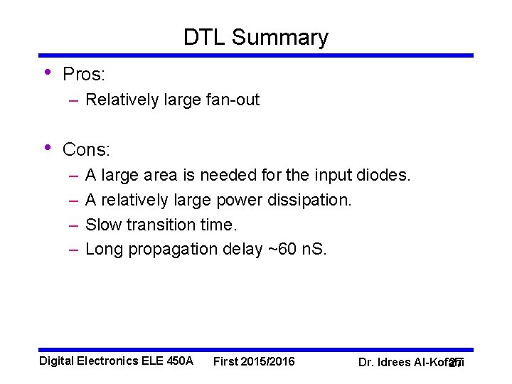
DTL Summary • Pros: – Relatively large fan-out • Cons: – – A large area is needed for the input diodes. A relatively large power dissipation. Slow transition time. Long propagation delay ~60 n. S. Digital Electronics ELE 450 A First 2015/2016 Dr. Idrees Al-Kofahi 27