ECE777 System Level Design and Automation 3 D


- Slides: 111

ECE-777 System Level Design and Automation 3 D integration. Reconfigurability and testing. Cristinel Ababei Electrical and Computer Department, North Dakota State University Spring 2012 1

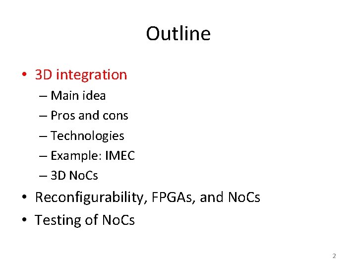
Outline • 3 D integration – Main idea – Pros and cons – Technologies – Example: IMEC – 3 D No. Cs • Reconfigurability, FPGAs, and No. Cs • Testing of No. Cs 2

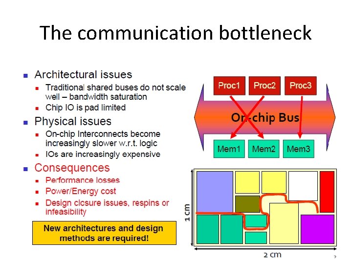
The communication bottleneck 3

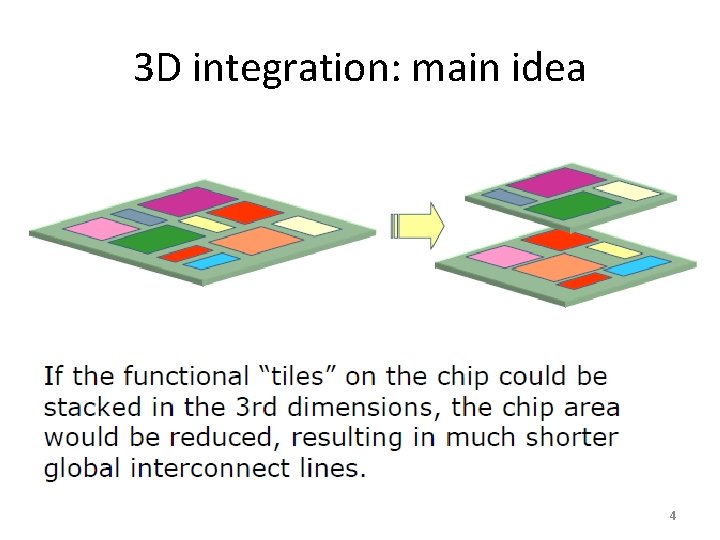
3 D integration: main idea 4

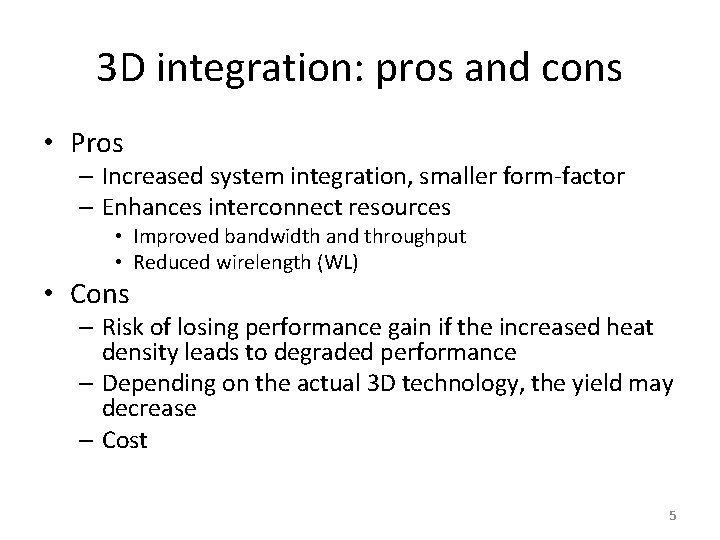
3 D integration: pros and cons • Pros – Increased system integration, smaller form-factor – Enhances interconnect resources • Improved bandwidth and throughput • Reduced wirelength (WL) • Cons – Risk of losing performance gain if the increased heat density leads to degraded performance – Depending on the actual 3 D technology, the yield may decrease – Cost 5

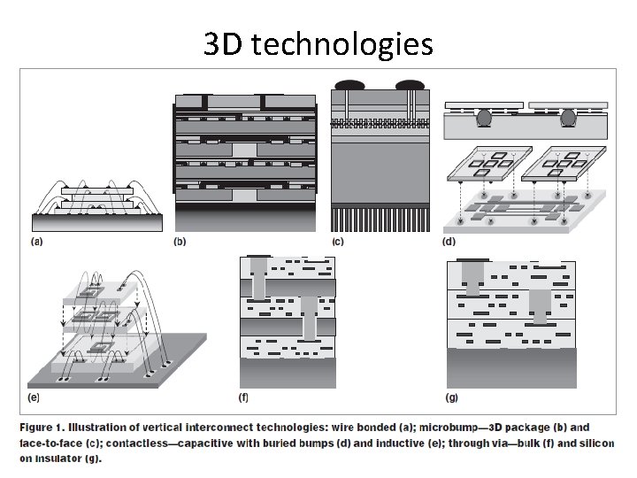
3 D technologies 6

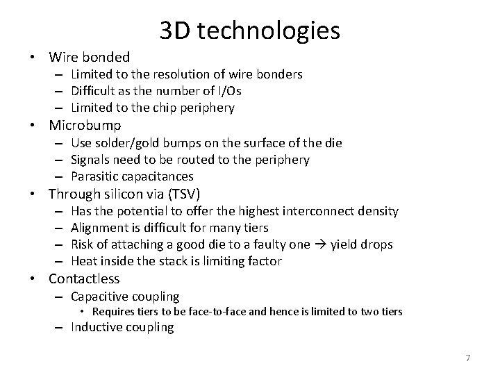
3 D technologies • Wire bonded – Limited to the resolution of wire bonders – Difficult as the number of I/Os – Limited to the chip periphery • Microbump – Use solder/gold bumps on the surface of the die – Signals need to be routed to the periphery – Parasitic capacitances • Through silicon via (TSV) – – Has the potential to offer the highest interconnect density Alignment is difficult for many tiers Risk of attaching a good die to a faulty one yield drops Heat inside the stack is limiting factor • Contactless – Capacitive coupling • Requires tiers to be face-to-face and hence is limited to two tiers – Inductive coupling 7

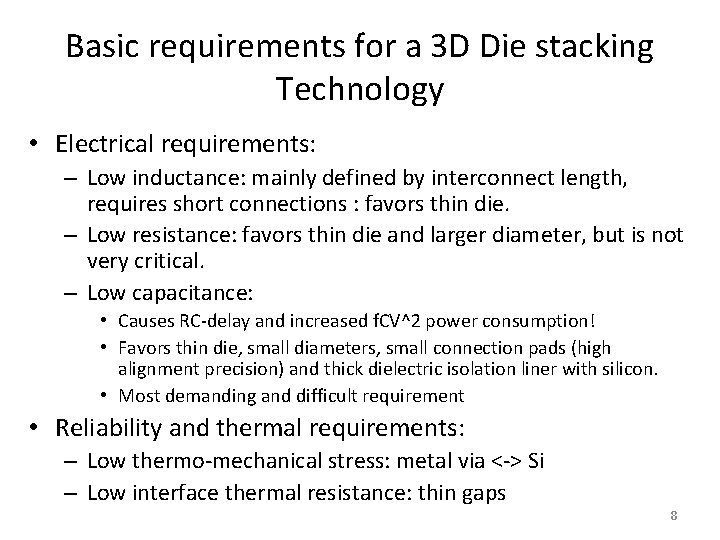
Basic requirements for a 3 D Die stacking Technology • Electrical requirements: – Low inductance: mainly defined by interconnect length, requires short connections : favors thin die. – Low resistance: favors thin die and larger diameter, but is not very critical. – Low capacitance: • Causes RC-delay and increased f. CV^2 power consumption! • Favors thin die, small diameters, small connection pads (high alignment precision) and thick dielectric isolation liner with silicon. • Most demanding and difficult requirement • Reliability and thermal requirements: – Low thermo-mechanical stress: metal via <-> Si – Low interface thermal resistance: thin gaps 8

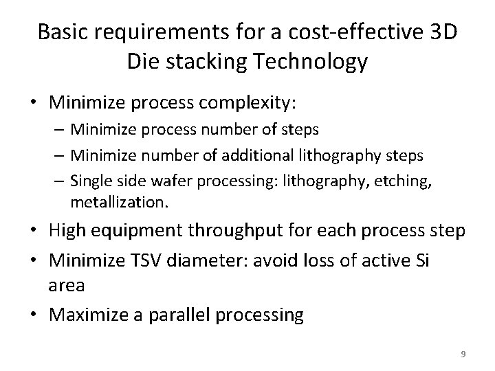
Basic requirements for a cost-effective 3 D Die stacking Technology • Minimize process complexity: – Minimize process number of steps – Minimize number of additional lithography steps – Single side wafer processing: lithography, etching, metallization. • High equipment throughput for each process step • Minimize TSV diameter: avoid loss of active Si area • Maximize a parallel processing 9

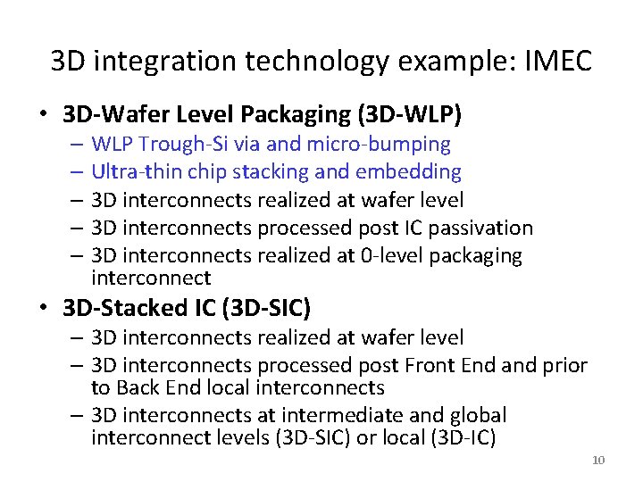
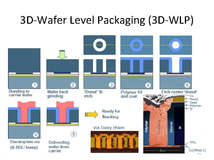
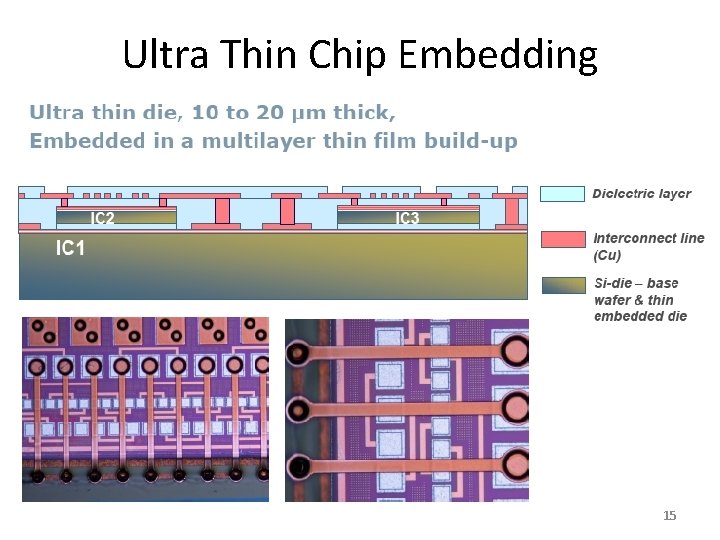
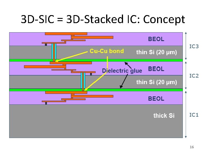
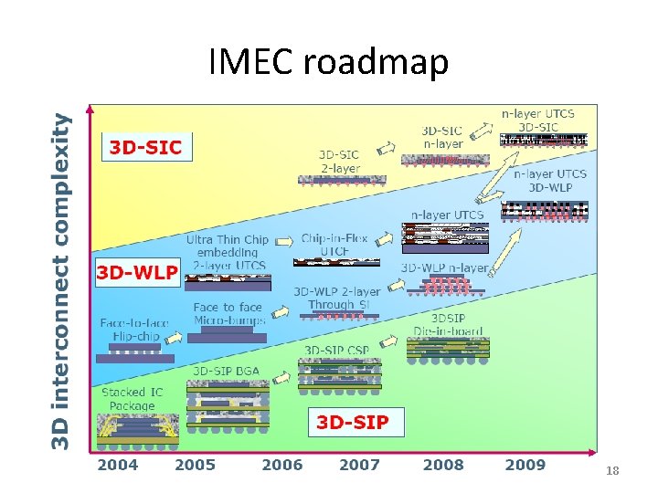
3 D integration technology example: IMEC • 3 D-Wafer Level Packaging (3 D-WLP) – WLP Trough-Si via and micro-bumping – Ultra-thin chip stacking and embedding – 3 D interconnects realized at wafer level – 3 D interconnects processed post IC passivation – 3 D interconnects realized at 0 -level packaging interconnect • 3 D-Stacked IC (3 D-SIC) – 3 D interconnects realized at wafer level – 3 D interconnects processed post Front End and prior to Back End local interconnects – 3 D interconnects at intermediate and global interconnect levels (3 D-SIC) or local (3 D-IC) 10

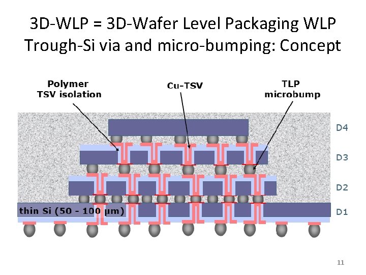
3 D-WLP = 3 D-Wafer Level Packaging WLP Trough-Si via and micro-bumping: Concept 11

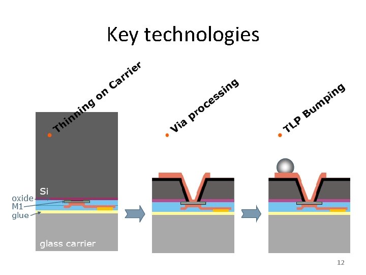
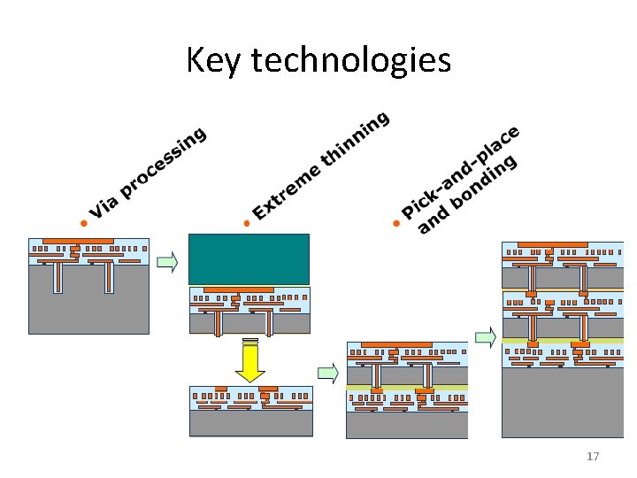
Key technologies 12

3 D-Wafer Level Packaging (3 D-WLP) 13

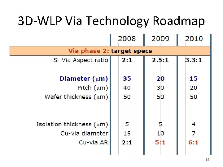
3 D-WLP Via Technology Roadmap 14

Ultra Thin Chip Embedding 15

3 D-SIC = 3 D-Stacked IC: Concept 16

Key technologies 17

IMEC roadmap 18

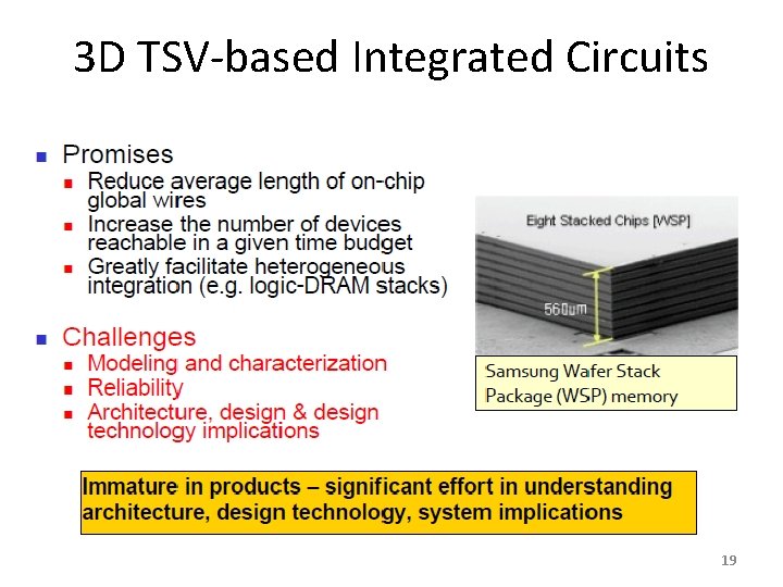
3 D TSV-based Integrated Circuits 19

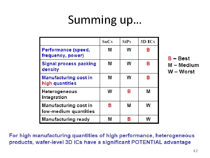
Summing up… Good power and speed Area overhead is significant Reliability not ideal (fabrication and aging) Synchronization is hard (skew minimization across layers) • Therefore: • • – Cost and design effort are not trivial – Not just another dimension for wiring (as of today) – Need a sistematic way to deal with non-ideality 20

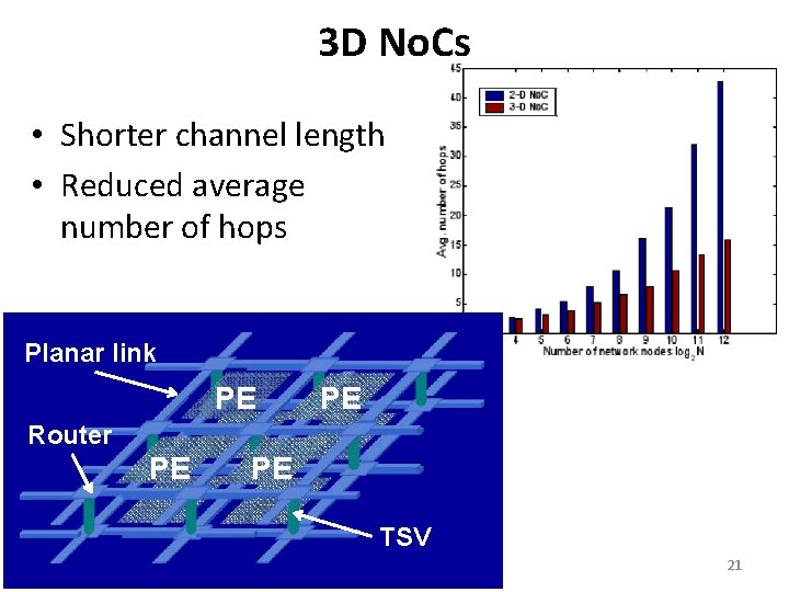
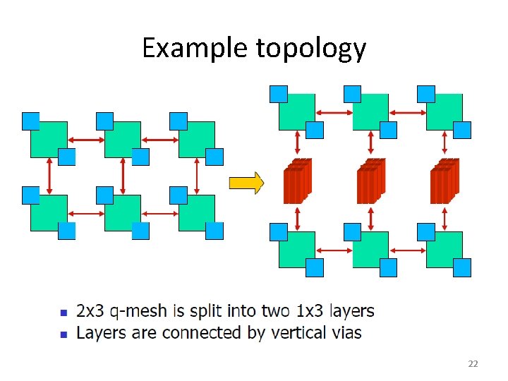
3 D No. Cs • Shorter channel length • Reduced average number of hops Planar link PE PE Router PE PE TSV 21

Example topology 22

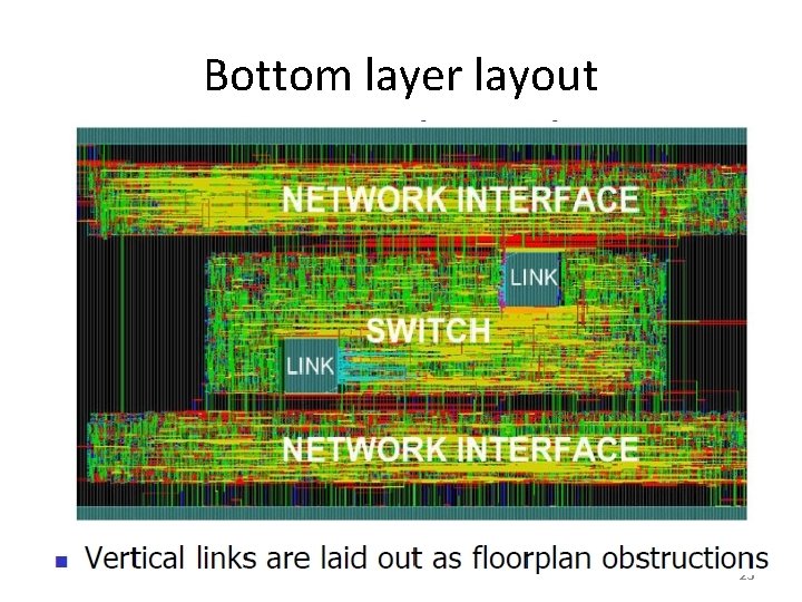
Bottom layer layout 23

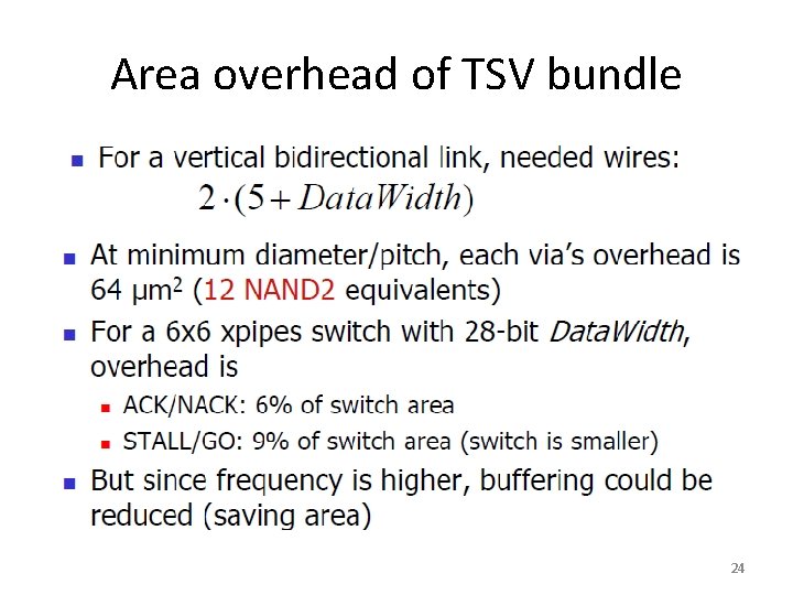
Area overhead of TSV bundle 24

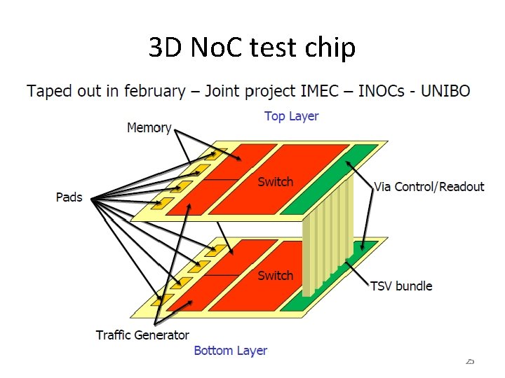
3 D No. C test chip 25

Design challenges • • Mesochronous Synchronization Performance Analysis Reliability Enhancement 3 D No. C Topology Synthesis 26

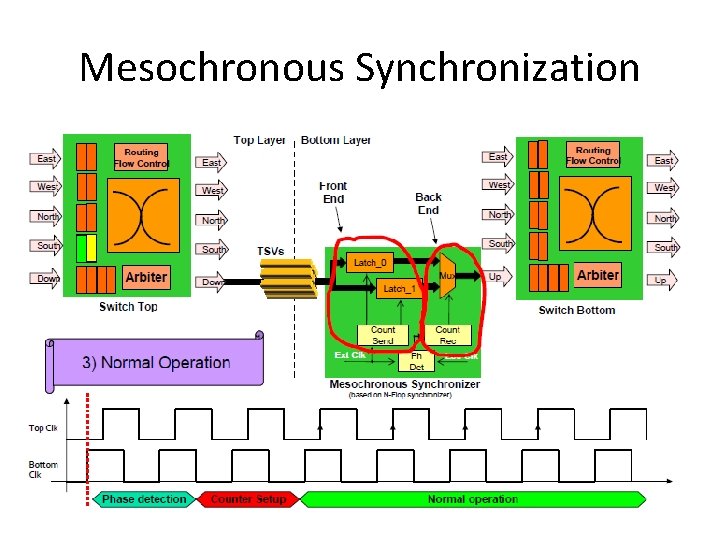
Mesochronous Synchronization 27

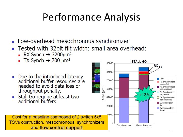
Performance Analysis 28

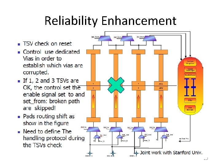
Reliability Enhancement 29

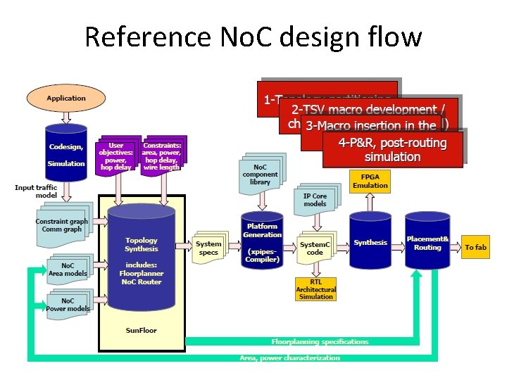
Reference No. C design flow 30

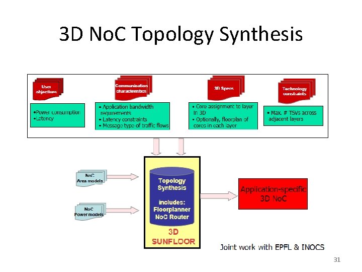
3 D No. C Topology Synthesis 31

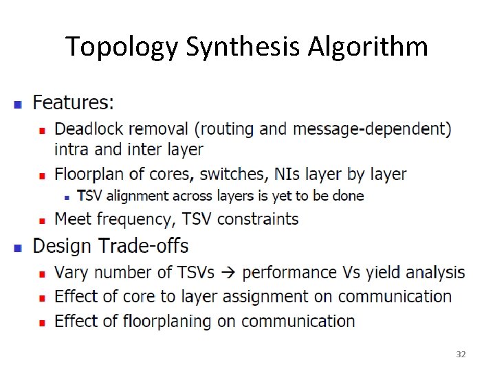
Topology Synthesis Algorithm 32

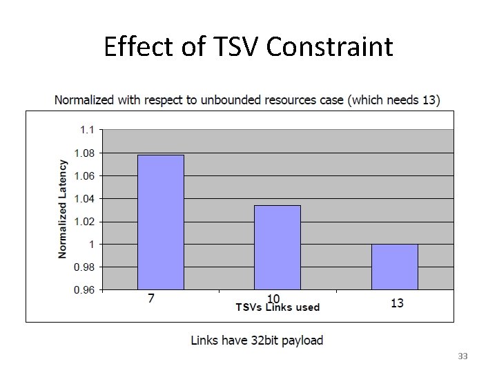
Effect of TSV Constraint 33

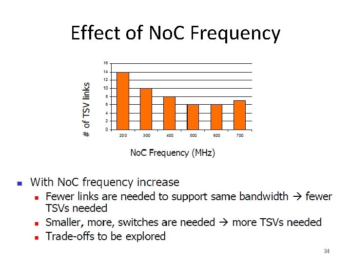
Effect of No. C Frequency 34

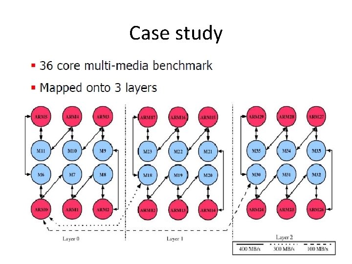
Case study 35

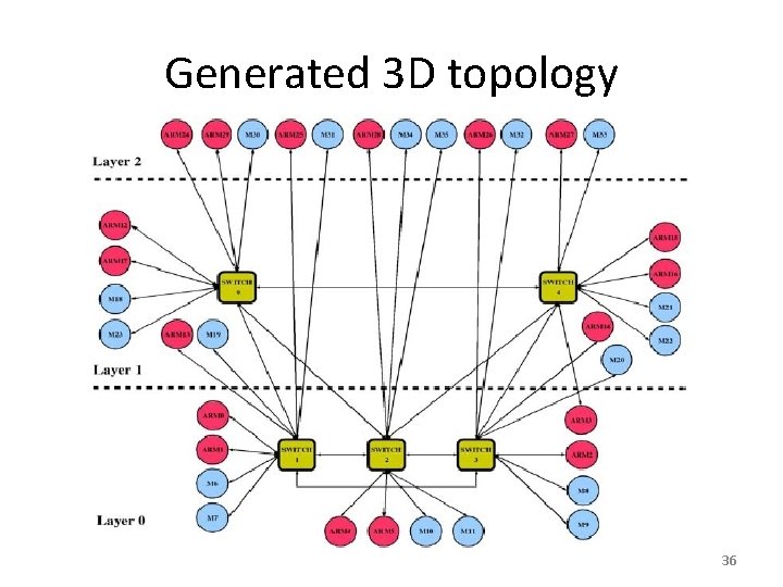
Generated 3 D topology 36

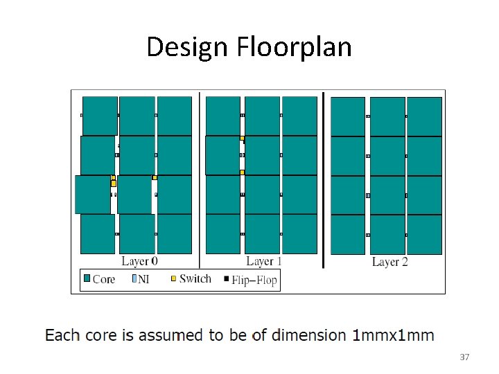
Design Floorplan 37

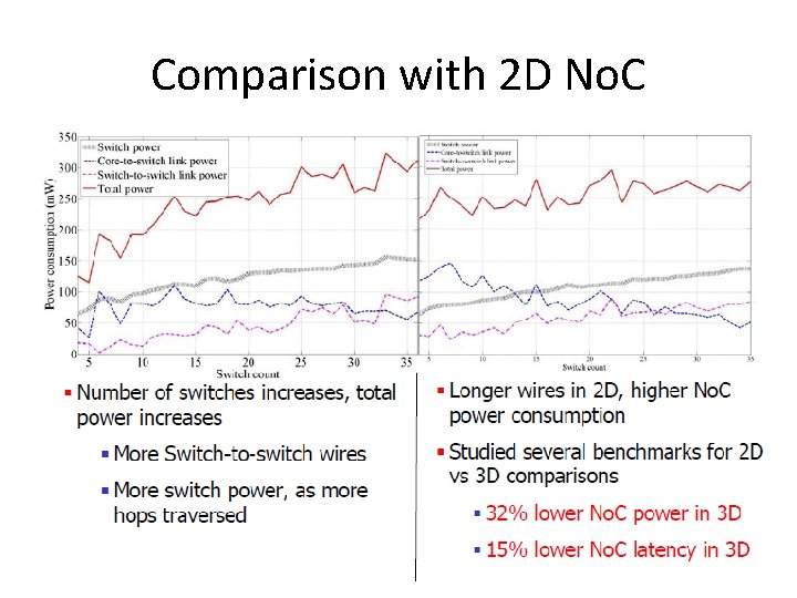
Comparison with 2 D No. C 38

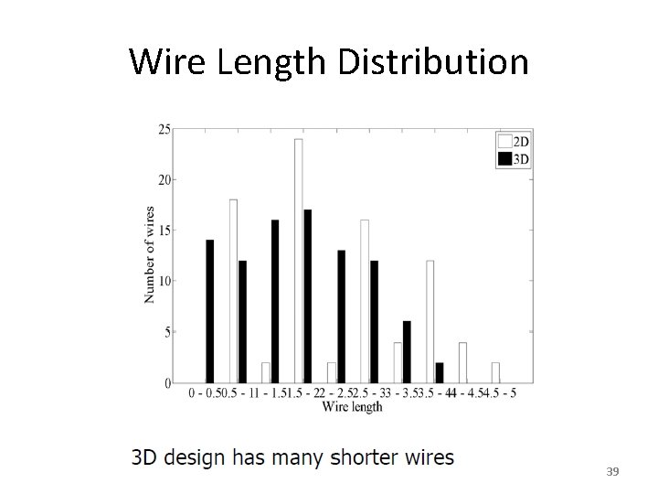
Wire Length Distribution 39

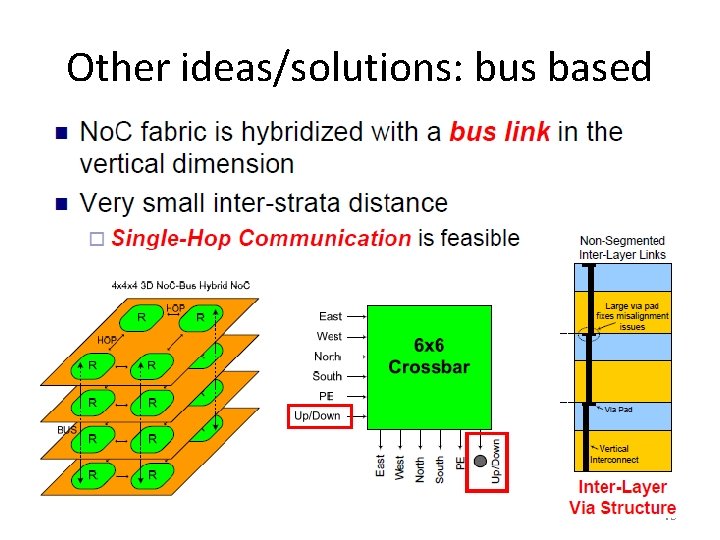
Other ideas/solutions: bus based 40

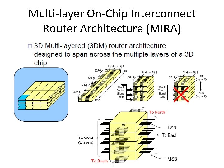
Multi-layer On-Chip Interconnect Router Architecture (MIRA) 41

Summing up… 42

Summing up… 43

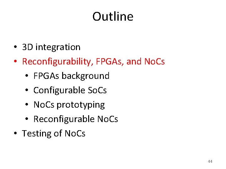
Outline • 3 D integration • Reconfigurability, FPGAs, and No. Cs • FPGAs background • Configurable So. Cs • No. Cs prototyping • Reconfigurable No. Cs • Testing of No. Cs 44

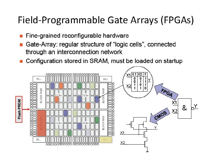
Field-Programmable Gate Arrays (FPGAs) 45

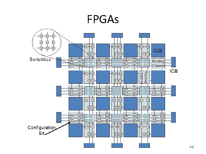
FPGAs 46

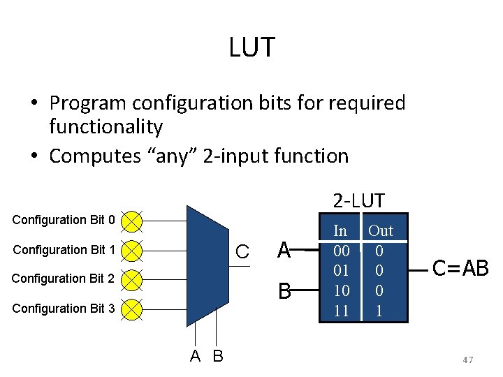
LUT • Program configuration bits for required functionality • Computes “any” 2 -input function 2 -LUT Configuration Bit 0 C Configuration Bit 1 Configuration Bit 2 A B Configuration Bit 3 A B In 00 01 10 11 Out 0 0 0 1 C=AB 47

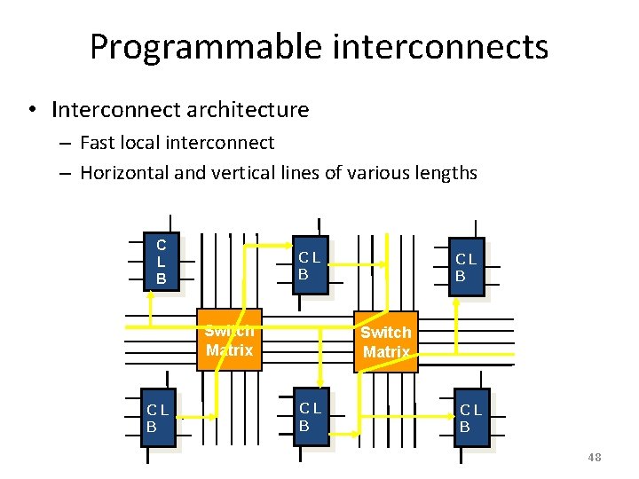
Programmable interconnects • Interconnect architecture – Fast local interconnect – Horizontal and vertical lines of various lengths C L B CL B Switch Matrix CL B 48

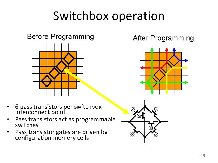
Switchbox operation Before Programming After Programming • 6 pass transistors per switchbox interconnect point • Pass transistors act as programmable switches • Pass transistor gates are driven by configuration memory cells 49

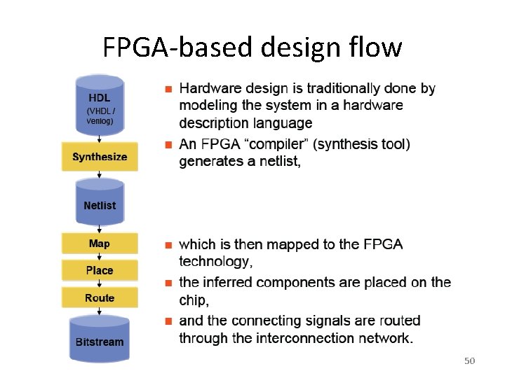
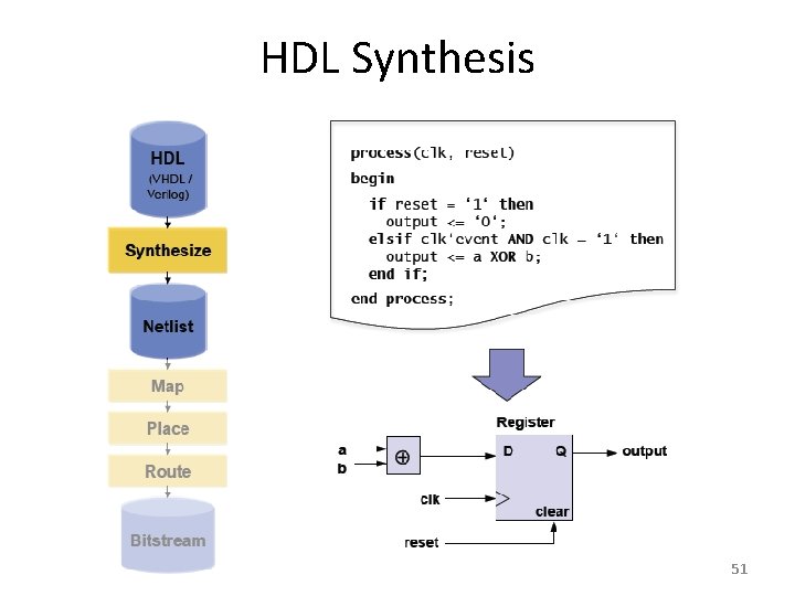
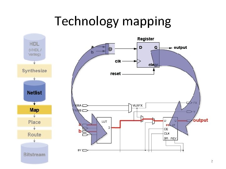
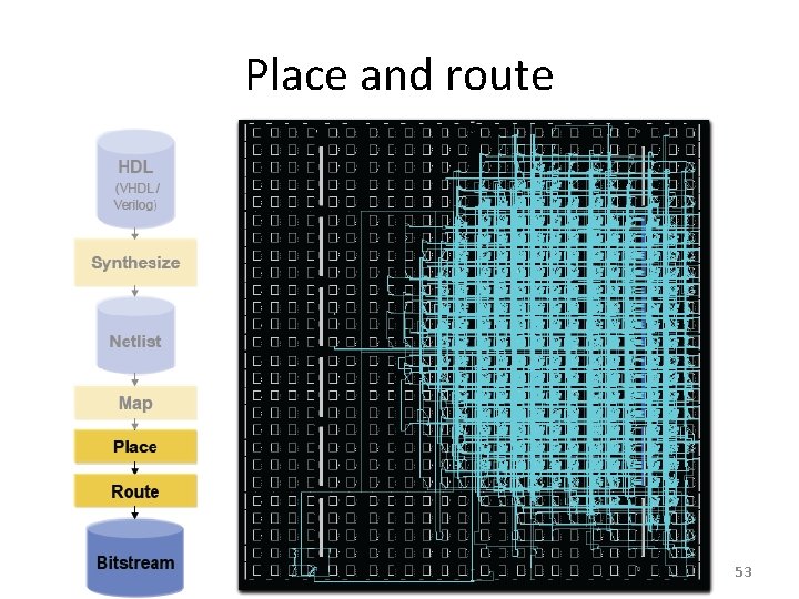
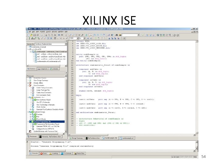
FPGA-based design flow 50

HDL Synthesis 51

Technology mapping 52

Place and route 53

XILINX ISE 54

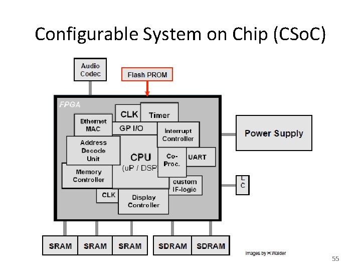
Configurable System on Chip (CSo. C) 55

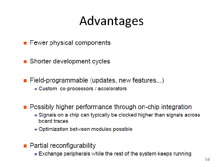
Advantages 56

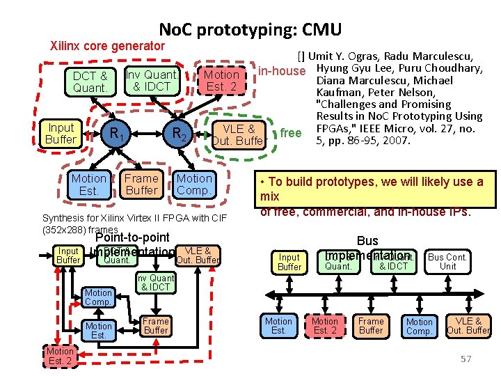
No. C prototyping: CMU Xilinx core generator Inv Quant. & IDCT & Quant. Input Buffer R 1 Motion Est. R 2 Frame Buffer [] Umit Y. Ogras, Radu Marculescu, in-house Hyung Gyu Lee, Puru Choudhary, Motion Diana Marculescu, Michael Est. 2 Kaufman, Peter Nelson, "Challenges and Promising Results in No. C Prototyping Using VLE & free FPGAs, " IEEE Micro, vol. 27, no. 5, pp. 86 -95, 2007. Out. Buffer Motion Comp. Synthesis for Xilinx Virtex II FPGA with CIF (352 x 288) frames Input Buffer Point-to-point DCT & Implementation Quant. Motion Comp. Motion Est. 2 VLE & Out. Buffer • To build prototypes, we will likely use a mix of free, commercial, and in-house IPs. Input Buffer Bus Implementation Inv Quant. DCT & Quant. & IDCT Bus Cont. Unit Inv Quant. & IDCT Frame Buffer Motion Est. 2 Frame Buffer Motion Comp. VLE & Out. Buffer 57

Recore’s reconfigurable system • Recore Systems – http: //www. recoresystems. com • Reconfigurable computing platforms 58

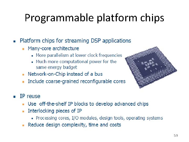
Programmable platform chips 59

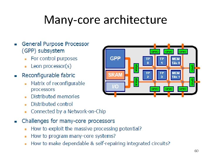
Many-core architecture 60

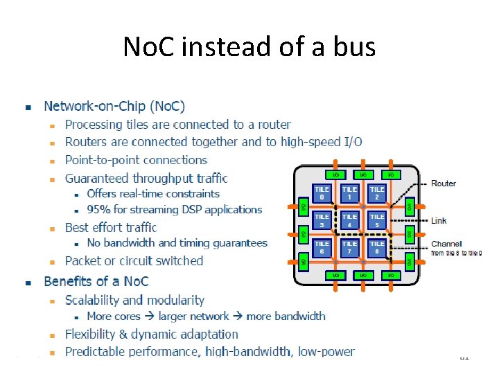
No. C instead of a bus 61

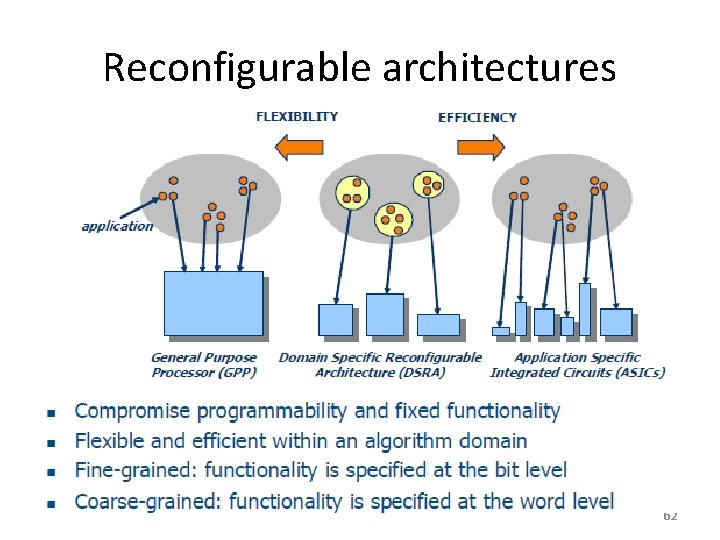
Reconfigurable architectures 62

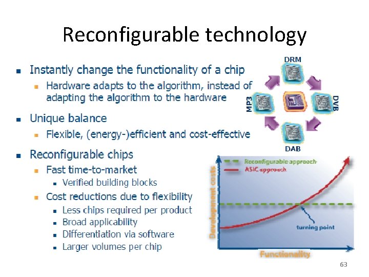
Reconfigurable technology 63

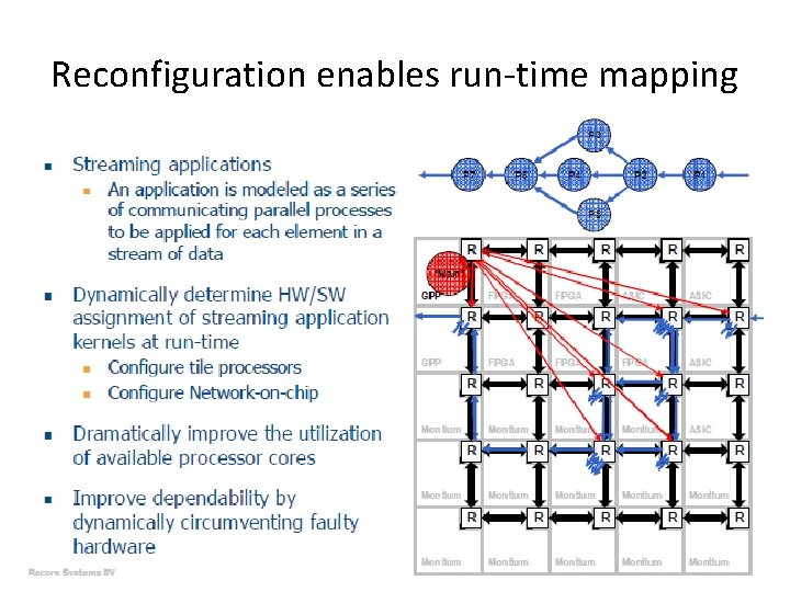
Reconfiguration enables run-time mapping 64

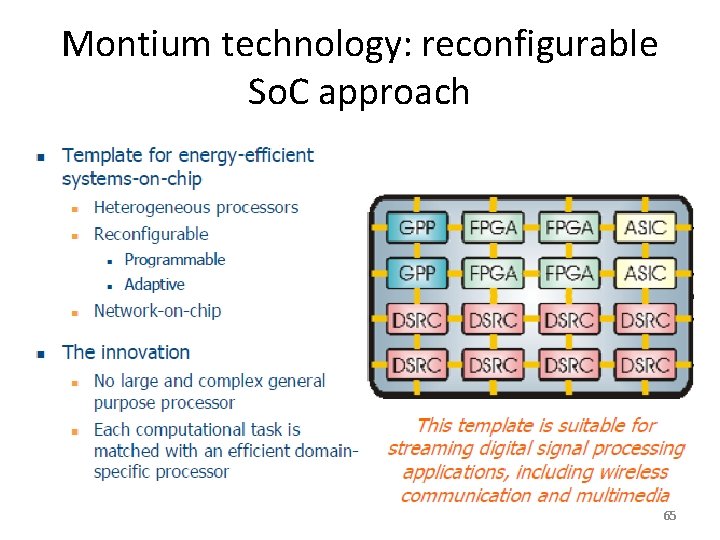
Montium technology: reconfigurable So. C approach 65

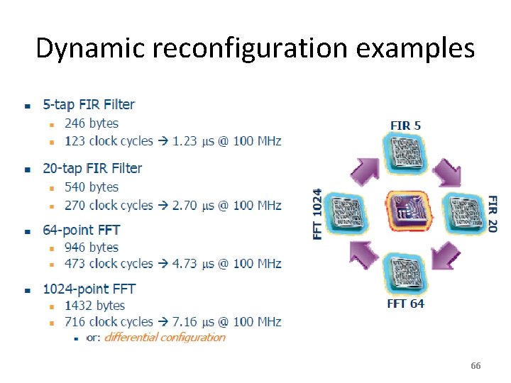
Dynamic reconfiguration examples 66

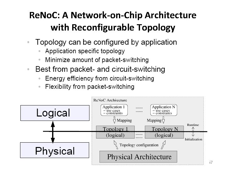
Re. No. C: A Network-on-Chip Architecture with Reconfigurable Topology 67

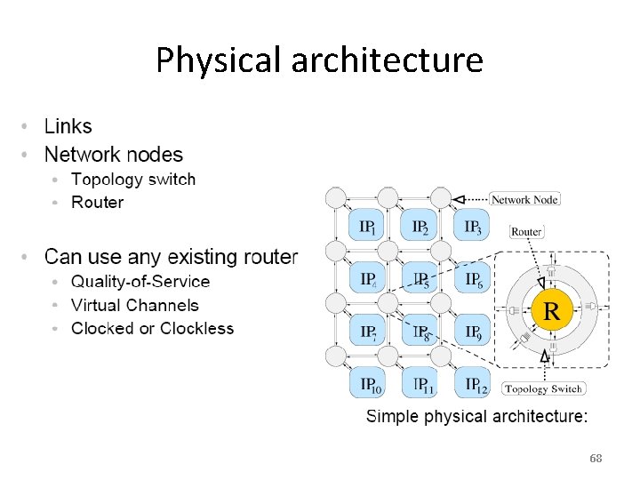
Physical architecture 68

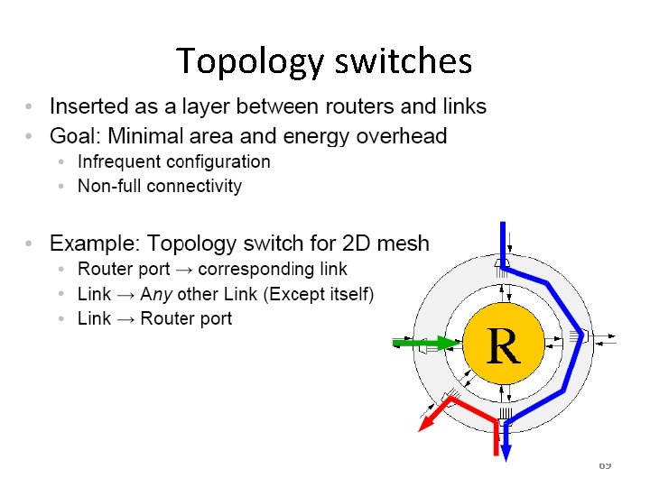
Topology switches 69

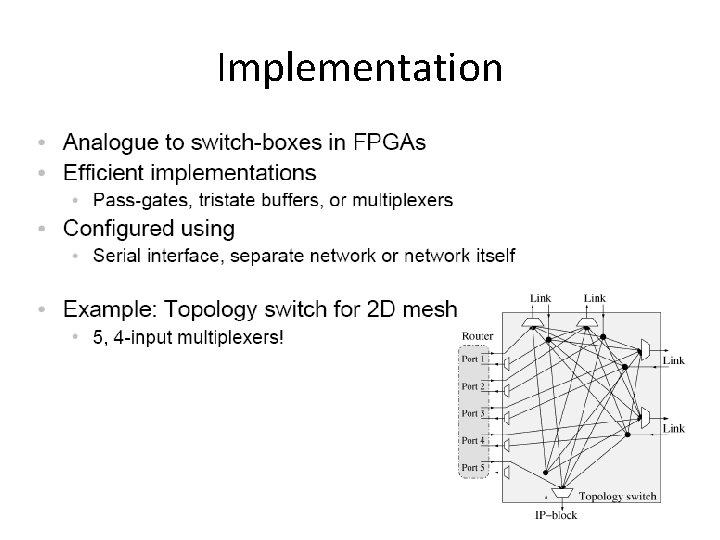
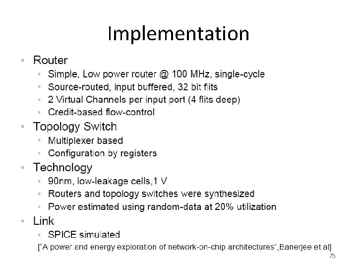
Implementation 70

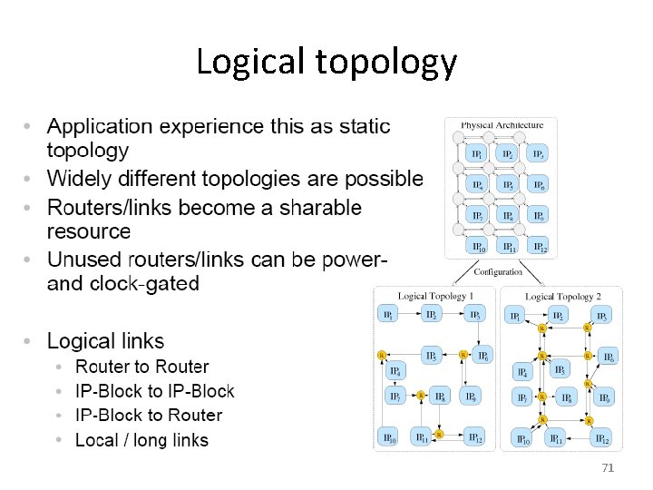
Logical topology 71

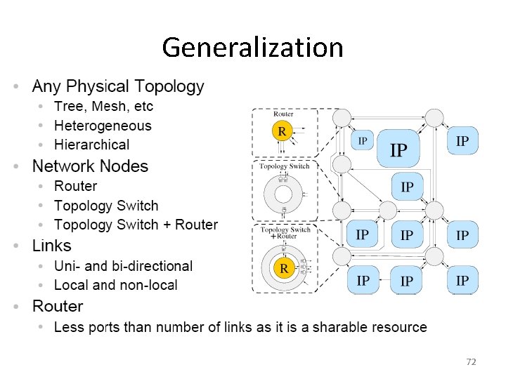
Generalization 72

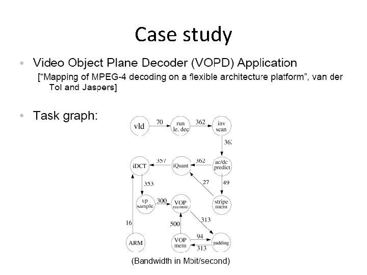
Case study 73

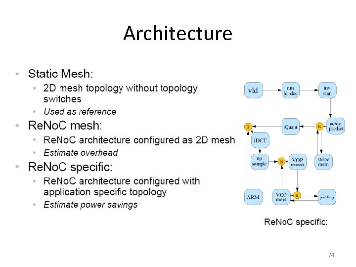
Architecture 74

Implementation 75

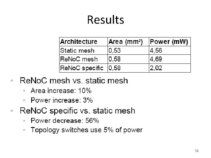
Results 76

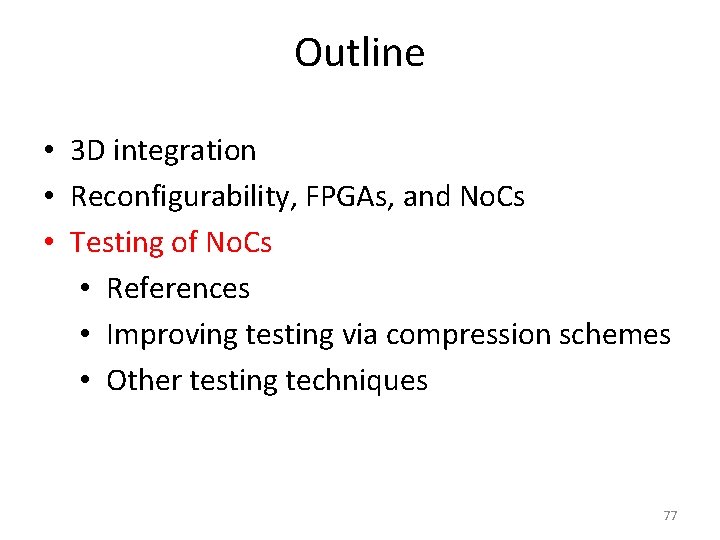
Outline • 3 D integration • Reconfigurability, FPGAs, and No. Cs • Testing of No. Cs • References • Improving testing via compression schemes • Other testing techniques 77

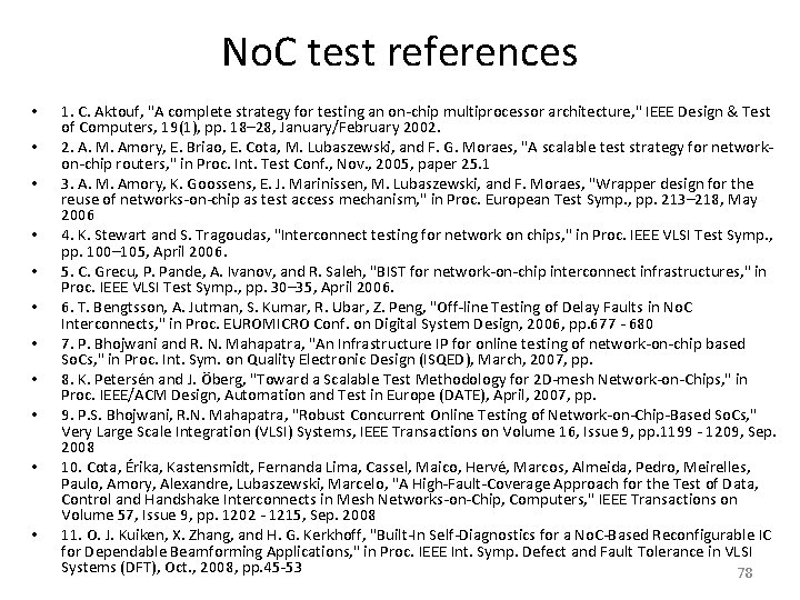
No. C test references • • • 1. C. Aktouf, "A complete strategy for testing an on-chip multiprocessor architecture, " IEEE Design & Test of Computers, 19(1), pp. 18– 28, January/February 2002. 2. A. M. Amory, E. Briao, E. Cota, M. Lubaszewski, and F. G. Moraes, "A scalable test strategy for networkon-chip routers, " in Proc. Int. Test Conf. , Nov. , 2005, paper 25. 1 3. A. M. Amory, K. Goossens, E. J. Marinissen, M. Lubaszewski, and F. Moraes, "Wrapper design for the reuse of networks-on-chip as test access mechanism, " in Proc. European Test Symp. , pp. 213– 218, May 2006 4. K. Stewart and S. Tragoudas, "Interconnect testing for network on chips, " in Proc. IEEE VLSI Test Symp. , pp. 100– 105, April 2006. 5. C. Grecu, P. Pande, A. Ivanov, and R. Saleh, "BIST for network-on-chip interconnect infrastructures, " in Proc. IEEE VLSI Test Symp. , pp. 30– 35, April 2006. 6. T. Bengtsson, A. Jutman, S. Kumar, R. Ubar, Z. Peng, "Off-line Testing of Delay Faults in No. C Interconnects, " in Proc. EUROMICRO Conf. on Digital System Design, 2006, pp. 677 - 680 7. P. Bhojwani and R. N. Mahapatra, "An Infrastructure IP for online testing of network-on-chip based So. Cs, " in Proc. Int. Sym. on Quality Electronic Design (ISQED), March, 2007, pp. 8. K. Petersén and J. Öberg, "Toward a Scalable Test Methodology for 2 D-mesh Network-on-Chips, " in Proc. IEEE/ACM Design, Automation and Test in Europe (DATE), April, 2007, pp. 9. P. S. Bhojwani, R. N. Mahapatra, "Robust Concurrent Online Testing of Network-on-Chip-Based So. Cs, " Very Large Scale Integration (VLSI) Systems, IEEE Transactions on Volume 16, Issue 9, pp. 1199 - 1209, Sep. 2008 10. Cota, Érika, Kastensmidt, Fernanda Lima, Cassel, Maico, Hervé, Marcos, Almeida, Pedro, Meirelles, Paulo, Amory, Alexandre, Lubaszewski, Marcelo, "A High-Fault-Coverage Approach for the Test of Data, Control and Handshake Interconnects in Mesh Networks-on-Chip, Computers, " IEEE Transactions on Volume 57, Issue 9, pp. 1202 - 1215, Sep. 2008 11. O. J. Kuiken, X. Zhang, and H. G. Kerkhoff, "Built-In Self-Diagnostics for a No. C-Based Reconfigurable IC for Dependable Beamforming Applications, " in Proc. IEEE Int. Symp. Defect and Fault Tolerance in VLSI Systems (DFT), Oct. , 2008, pp. 45 -53 78

No. C test references • • • 12. M. Sedghi, E. Koopahi, A. Alaghi, M. Fathy, and Z. Navabi, "An No. C Test Strategy Based on Flooding with Power, Test Time and Coverage Considerations, " in Proc. Int. Conf. on VLSI Design, 2008, pp. 409 -414 13. X. -T. Tran, Y. Thonnart, J. Durupt, V. Beroulle, and C. Robach, "A Design-for-Test Implementation of an Asynchronous Network-on-Chip Architecture and its Associated Test Pattern Generation and Application, " in Proc. Int. Symp. on Networks-on-Chip, 2008, pp. 149 -158 14. J. Dalmasso 1, É. Cota, M. -L. Flottes, and B. Rouzeyre, "Improving the Test of No. C-based So. Cs with Help of Compression Schemes, " in Proc. IEEE Computer Society Annual Symp. on VLSI, 2008, pp. 139 -144 15. B. -G. Ahn, J. -M. Jung, and J. -W. Chong, "Power-Aware Test Framework for Network-on-Chip, " in Proc. , Int. Conf. on Systems, 2008, pp. 103 -107 16. M. Hervé, É. Cota, F. L. Kastensmidt, and M. Lubaszewski, "Diagnosis of Interconnect Shorts in Mesh No. Cs, " in Proc. ACM/IEEE International Symposium on Network-on-Chip (No. CS), May 2009, pp. 256 - 265. 17. B. Vermeulen 1, K. Goossens, "A Network-on-Chip Monitoring Infrastructure for Communicationcentric Debug of Embedded Multi-Processor So. Cs, "in Proc. International Symposium on VLSI Design, Automation and Test (VLSI-DAT), May 2009, pp. 183 -186. 18. A. Eghbal, P. M. Yaghini, H. Pedram, and H. R. Zarandi, "Fault Injection-based Evaluation of a Synchronous No. C Router, " in IEEE International On-Line Testing Symposium (IOLTS), June 2009, pp. 212214. 19. J. Raik, V. Govind, and R. Ubar, "Design-for-testability-based external test and diagnosis of mesh-like network-on-a-chips, " in IET Computers & Digital Techniques, vo. 3, no. 5, pp. 476 - 486, Sep. 2009. 20. X. -T. Tran, Y. Thonnart, J. Durupt, V. Beroulle and C. Robach, "Design-for-test approach of an asynchronous network-on-chip architecture and its associated test pattern generation and application, " in IET Computers & Digital Techniques, vo. 3, no. 5, pp. 487 - 500, Sep. 2009. 21. H. -N. Liu, Y. -J. Huang, and J. -F. Li, "A built-in self-repair method for RAMs in mesh-based No. Cs, " in IEEE Int. Symp. on VLSI Design, Automation, and Test (VLSI-DAT), (Hsinchu), pp. -, Apr. 2009 22. S. -Y. Lin, C. -C. Hsu, and A. -Y. (Andy) Wu, "A Scalable Built-in Self-Test/Self-Diagnosis Architecture for 2 D-mesh Based Chip Multiprocessor Systems, " in Proc. IEEE International Symp. on Circuits and Systems (ISCAS), May, 2009, pp. 2317 -2320. 79

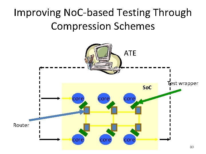
Improving No. C-based Testing Through Compression Schemes ATE So. C core core Test wrapper Router 80

No. C-based testing • Functional inputs and outputs are used during test, similarly standard So. C testing • The No. C will be used to transmit data from the ATE to the cores and vice-versa • Wrappers design – No. C protocol – 1500 -compliant 81

Approaches • Preemptive testing – One vector per message, non-reserved paths – Schedule next test-vector packet of a core as soon as a path is available – Length of the paths travelled by different tests to the same core can be different • Non-preemptive testing – All test-vectors in one message – Routing is done using dedicated paths, similar to circuit switching 82

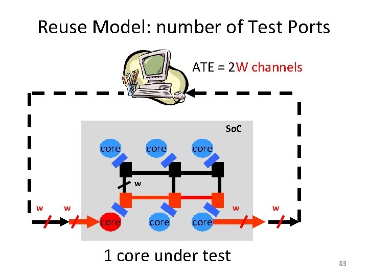
Reuse Model: number of Test Ports ATE = 2 W channels So. C core w w core 1 core under test 83

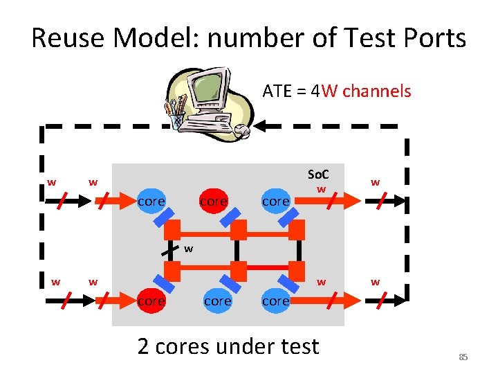
Observations • The main limitation for test time reduction is the number of test ports available • For non-preemptive testing, the problem is even more serious: the number of input and output test ports must be equal (so that a complete access path can be defined per core) • If extra pins can be added to the system to reduce test time, a more expensive ATE will be required 84

Reuse Model: number of Test Ports ATE = 4 W channels w So. C w core w w w core 2 cores under test 85

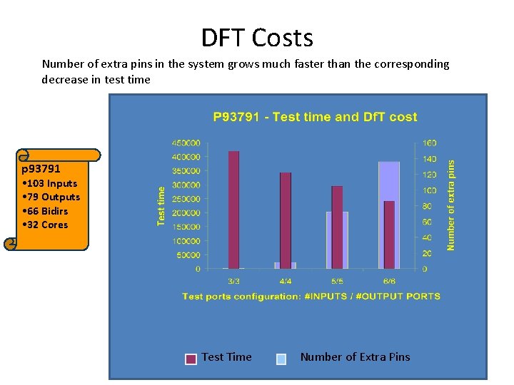
DFT Costs Number of extra pins in the system grows much faster than the corresponding decrease in test time p 93791 • 103 Inputs • 79 Outputs • 66 Bidirs • 32 Cores Test Time Number of Extra Pins 86

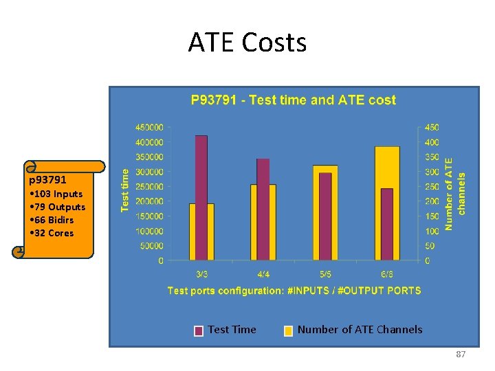
ATE Costs p 93791 • 103 Inputs • 79 Outputs • 66 Bidirs • 32 Cores Test Time Number of ATE Channels 87

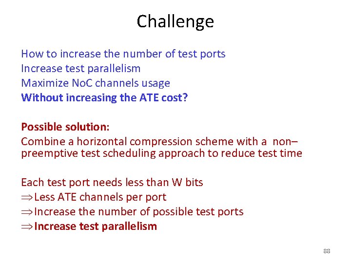
Challenge How to increase the number of test ports Increase test parallelism Maximize No. C channels usage Without increasing the ATE cost? Possible solution: Combine a horizontal compression scheme with a non– preemptive test scheduling approach to reduce test time Each test port needs less than W bits Þ Less ATE channels per port Þ Increase the number of possible test ports Þ Increase test parallelism 88

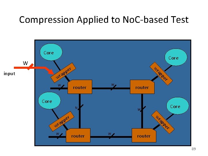
Compression Applied to No. C-based Test Core W wr input er p p er p ap a wr W W router Core N r pe ap W er p p wr a wr Core W router 89

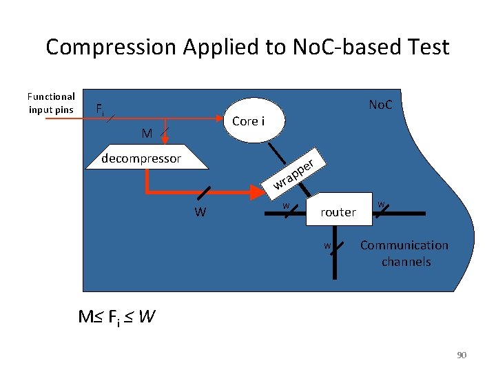
Compression Applied to No. C-based Test Functional input pins Fi No. C Core i M decompressor a wr W W r e pp router W W Communication channels M≤ Fi ≤ W 90

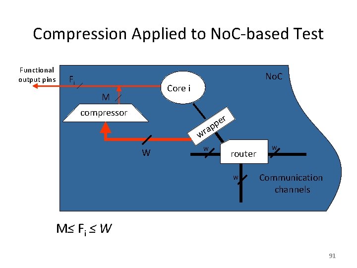
Compression Applied to No. C-based Test Functional output pins Fi No. C Core i M compressor a wr W W r e pp router W W Communication channels M≤ Fi ≤ W 91

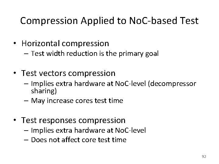
Compression Applied to No. C-based Test • Horizontal compression – Test width reduction is the primary goal • Test vectors compression – Implies extra hardware at No. C-level (decompressor sharing) – May increase cores test time • Test responses compression – Implies extra hardware at No. C-level – Does not affect core test time 92

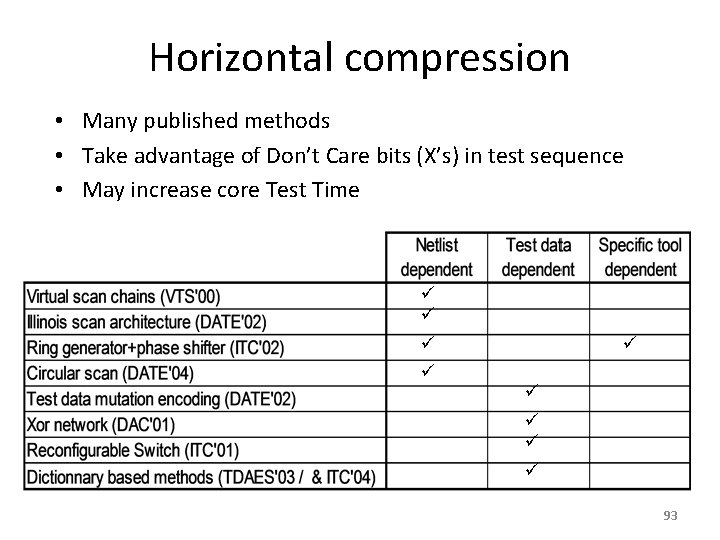
Horizontal compression • Many published methods • Take advantage of Don’t Care bits (X’s) in test sequence • May increase core Test Time 93

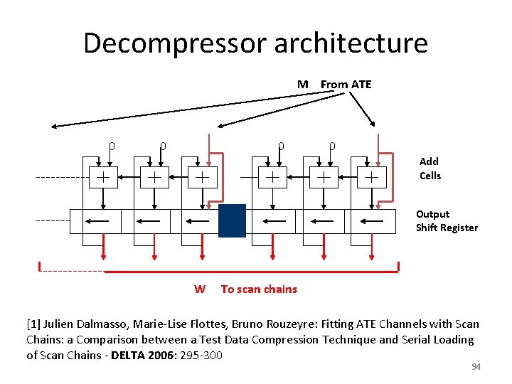
Decompressor architecture M From ATE 0 0 Add Cells Output Shift Register W To scan chains [1] Julien Dalmasso, Marie-Lise Flottes, Bruno Rouzeyre: Fitting ATE Channels with Scan Chains: a Comparison between a Test Data Compression Technique and Serial Loading of Scan Chains - DELTA 2006: 295 -300 94

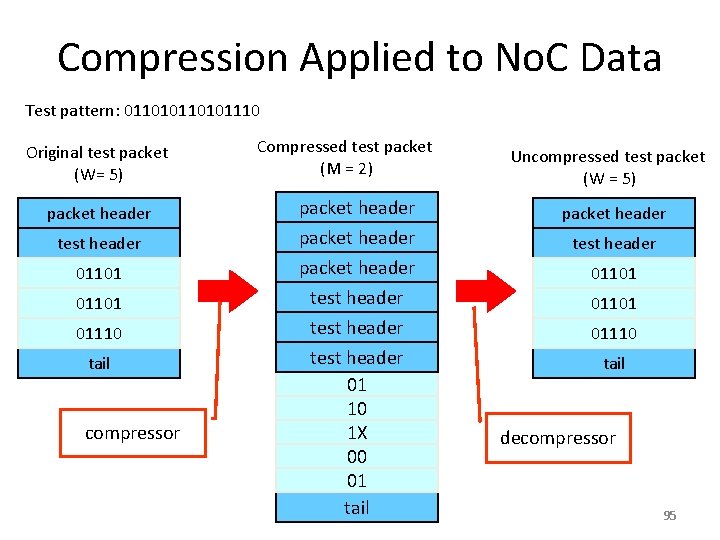
Compression Applied to No. C Data Test pattern: 0110101110 Original test packet (W= 5) packet header test header 01101 01110 tail compressor Compressed test packet (M = 2) Uncompressed test packet (W = 5) packet header test header 01 10 1 X 00 01 tail 01101 test header 01101 01110 tail decompressor 95

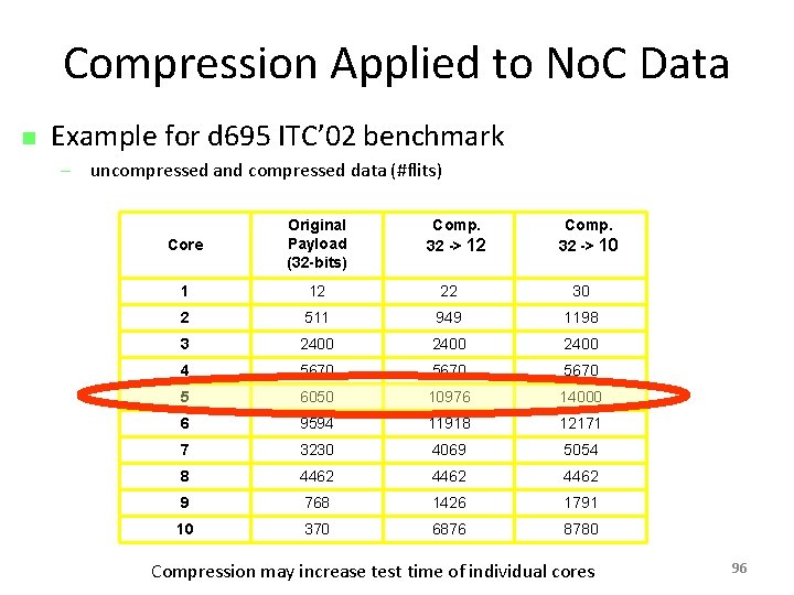
Compression Applied to No. C Data n Example for d 695 ITC’ 02 benchmark – uncompressed and compressed data (#flits) Core Original Payload (32 -bits) Comp. 32 -> 12 Comp. 32 -> 10 1 12 22 30 2 511 949 1198 3 2400 4 5670 5 6050 10976 14000 6 9594 11918 12171 7 3230 4069 5054 8 4462 9 768 1426 1791 10 370 6876 8780 Compression may increase test time of individual cores 96

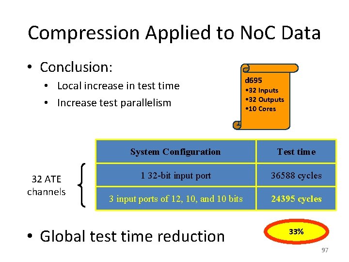
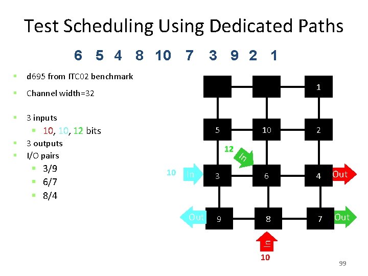
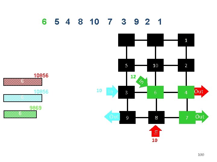
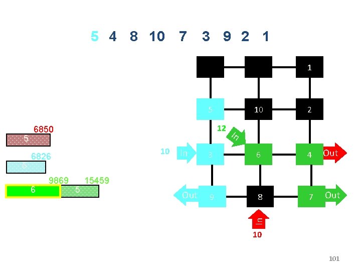
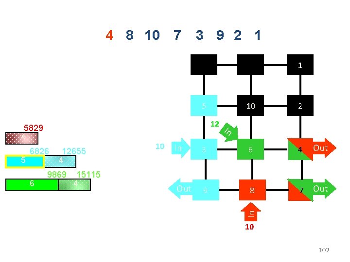
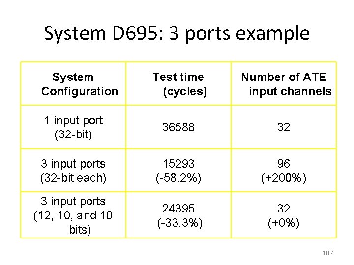
Compression Applied to No. C Data • Conclusion: • Local increase in test time • Increase test parallelism 32 ATE channels d 695 • 32 Inputs • 32 Outputs • 10 Cores System Configuration Test time 1 32 -bit input port 36588 cycles 3 input ports of 12, 10, and 10 bits 24395 cycles • Global test time reduction 33% 97

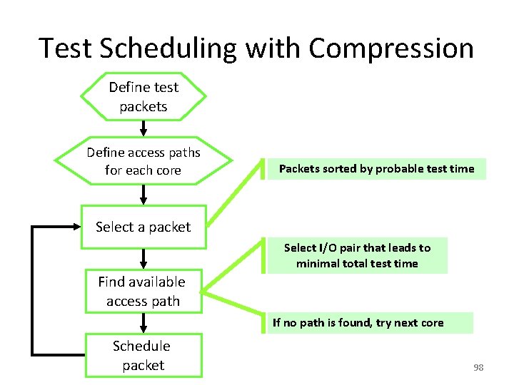
Test Scheduling with Compression Define test packets Define access paths for each core Packets sorted by probable test time Select a packet Select I/O pair that leads to minimal total test time Find available access path If no path is found, try next core Schedule packet 98

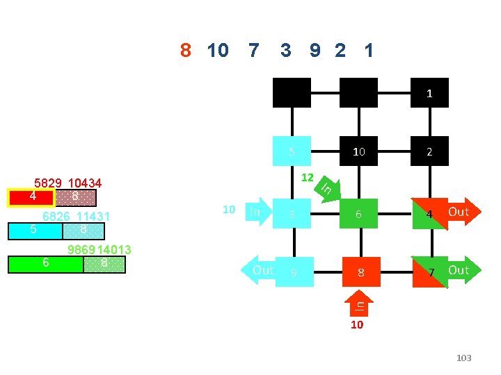
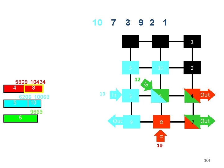
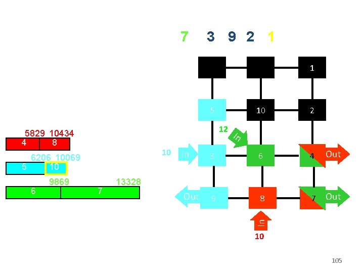
Test Scheduling Using Dedicated Paths 6 5 4 8 10 d 695 from ITC 02 benchmark § Channel width=32 § 3 inputs 1 5 § 10, 12 bits § § 3 9 2 1 3 outputs I/O pairs § 3/9 § 6/7 § 8/4 12 10 10 2 In In 3 6 4 Out 9 8 7 Out In § 7 10 99

6 5 4 8 10 7 3 9 2 1 1 5 6 6 10856 12 10 2 In In 3 6 4 Out 9 8 7 Out 9869 In 6 10856 10 10 100

5 4 8 10 7 3 9 2 1 1 5 5 10 6826 6 9869 5 2 In In 3 6 4 Out 9 8 7 Out 15459 In 5 12 6850 10 10 101

4 8 10 7 3 9 2 1 1 5 12 5 6826 6 12655 4 9869 15115 4 10 2 In In 3 6 4 Out 9 8 7 Out In 5829 4 10 10 102

8 10 7 3 9 2 1 1 5 6826 11431 5 8 6 9869 14013 8 12 10 2 In In 3 6 4 Out 9 8 7 Out In 5829 10434 4 8 10 10 103

10 7 3 9 2 1 1 5 5829 10434 4 8 6206 10069 5 10 10 2 In In 3 6 4 Out 9 8 7 Out 9869 In 6 12 10 10 104

7 3 9 2 1 1 5 12 5829 10434 4 8 10 6206 10069 5 10 7 2 In In 3 6 4 Out 9 8 7 Out 13328 In 6 9869 10 10 105

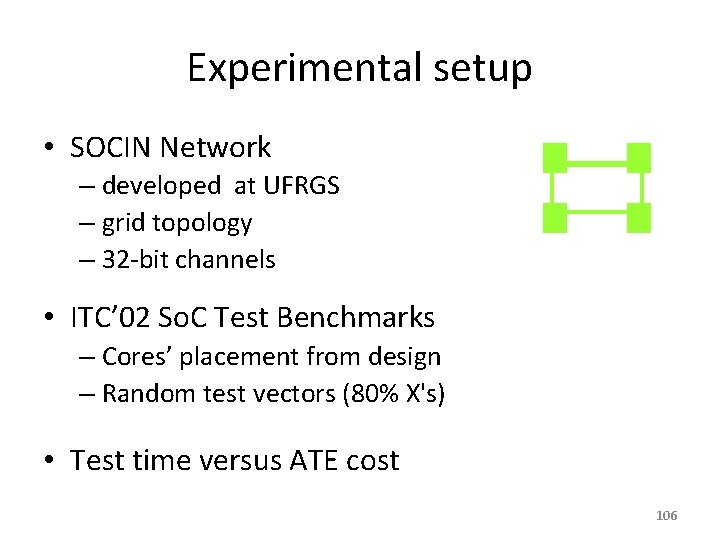
Experimental setup • SOCIN Network – developed at UFRGS – grid topology – 32 -bit channels • ITC’ 02 So. C Test Benchmarks – Cores’ placement from design – Random test vectors (80% X's) • Test time versus ATE cost 106

System D 695: 3 ports example System Configuration Test time (cycles) Number of ATE input channels 1 input port (32 -bit) 36588 32 3 input ports (32 -bit each) 15293 (-58. 2%) 96 (+200%) 3 input ports (12, 10, and 10 bits) 24395 (-33. 3%) 32 (+0%) 107

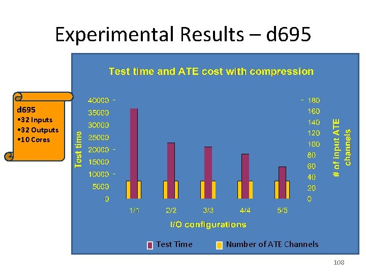
Experimental Results – d 695 • 32 Inputs • 32 Outputs • 10 Cores Test Time Number of ATE Channels 108

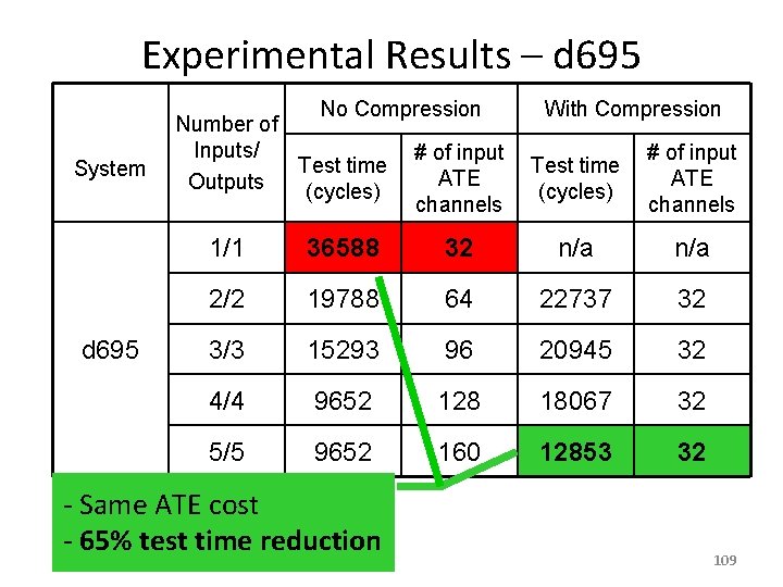
Experimental Results – d 695 No Compression System d 695 Number of Inputs/ Test time Outputs (cycles) With Compression # of input ATE channels Test time (cycles) # of input ATE channels 1/1 36588 32 n/a 2/2 19788 64 22737 32 3/3 15293 96 20945 32 4/4 9652 128 18067 32 5/5 9652 160 12853 32 - Same ATE cost - 65% test time reduction 109

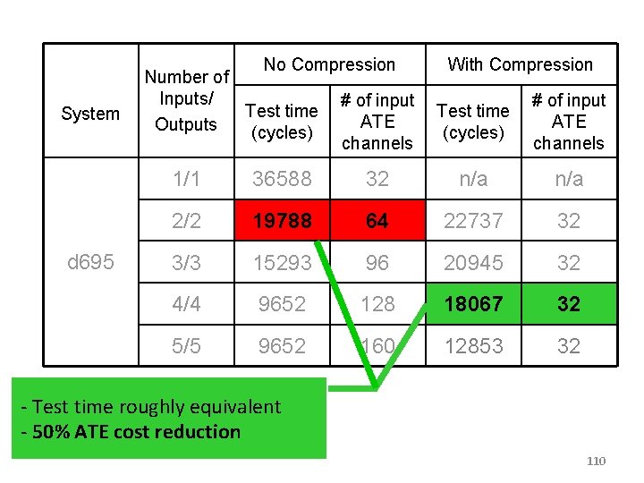
No Compression System d 695 Number of Inputs/ Test time Outputs (cycles) With Compression # of input ATE channels Test time (cycles) # of input ATE channels 1/1 36588 32 n/a 2/2 19788 64 22737 32 3/3 15293 96 20945 32 4/4 9652 128 18067 32 5/5 9652 160 12853 32 - Test time roughly equivalent - 50% ATE cost reduction 110

Summing up… • Combination of No. C-based testing and horizontal compression – Reduces So. C test time – Reduces ATE costs • Compression technique – compliant with So. C Testing • Future works – seek for the best partition of ATE channels into test interfaces at No. C-level – test time reduction / area overhead trade-off 111