ELEC 516 VLSI System Design and Design Automation
![More realistic H-tree [Restle 98] 42 ELEC 516/10 Lecture 6 More realistic H-tree [Restle 98] 42 ELEC 516/10 Lecture 6](https://slidetodoc.com/presentation_image_h/7937443dfa0ffc2895e125d336ef0aef/image-42.jpg)
- Slides: 56

ELEC 516 VLSI System Design and Design Automation Spring 2010 Lecture 6: Timing and Clocking Issues Reading Assignment: Rabaey: Chapter 10 Note: some of the figures in this slide set are adapted from the slide set of “ Digital Integrated Circuits” by Rabaey et. al. , Copyright 2002 1 ELEC 516/10 Lecture 6

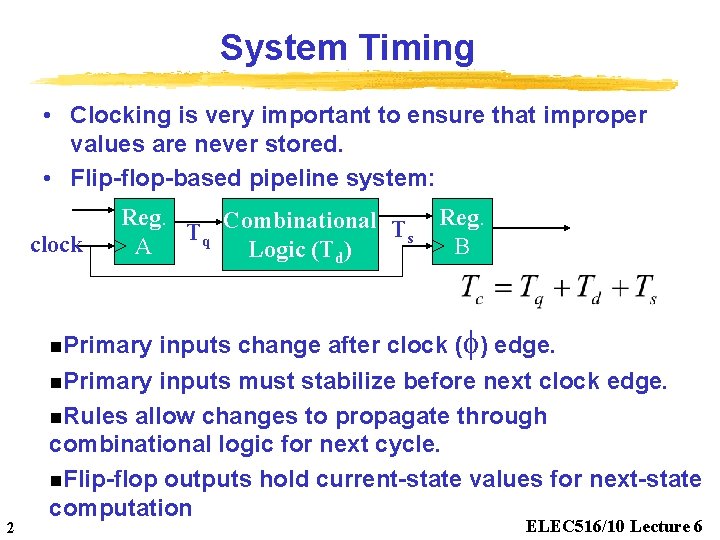
System Timing • Clocking is very important to ensure that improper values are never stored. • Flip-flop-based pipeline system: clock Reg. Tq Combinational Ts A Logic (Td) Reg. B inputs change after clock ( ) edge. n. Primary inputs must stabilize before next clock edge. n. Rules allow changes to propagate through combinational logic for next cycle. n. Flip-flop outputs hold current-state values for next-state computation n. Primary 2 ELEC 516/10 Lecture 6

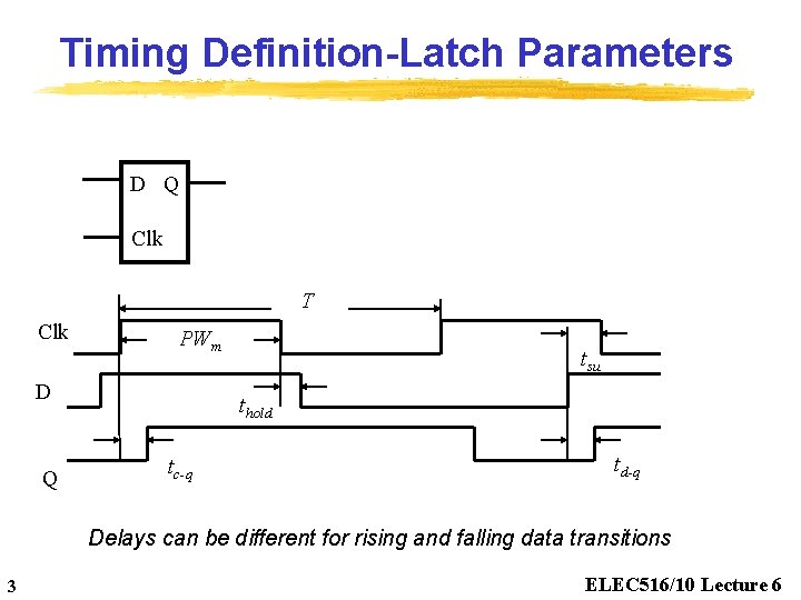
Timing Definition-Latch Parameters D Q Clk T Clk PWm D Q tsu thold tc-q td-q Delays can be different for rising and falling data transitions 3 ELEC 516/10 Lecture 6

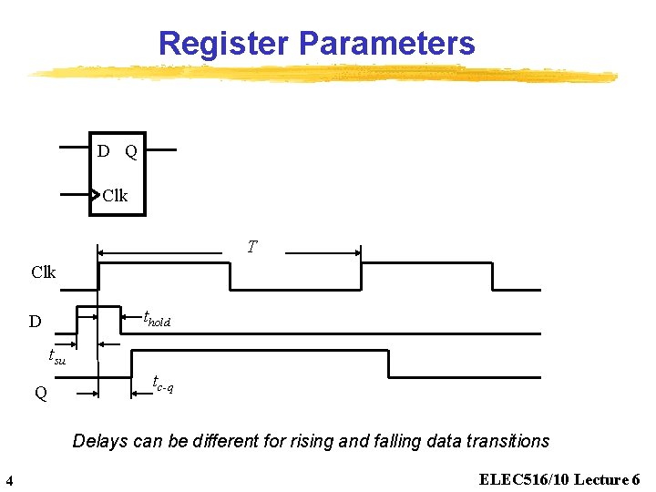
Register Parameters D Q Clk T Clk thold D tsu Q tc-q Delays can be different for rising and falling data transitions 4 ELEC 516/10 Lecture 6

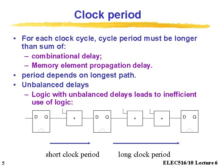
Clock period • For each clock cycle, cycle period must be longer than sum of: – combinational delay; – Memory element propagation delay. • period depends on longest path. • Unbalanced delays – Logic with unbalanced delays leads to inefficient use of logic: short clock period 5 long clock period ELEC 516/10 Lecture 6

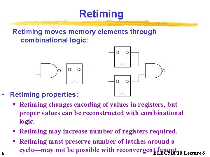
Retiming moves memory elements through combinational logic: • Retiming properties: § Retiming changes encoding of values in registers, but proper values can be reconstructed with combinational logic. § Retiming may increase number of registers required. § Retiming must preserve number of latches around a cycle—may not be possible with reconvergent. ELEC 516/10 fanout. Lecture 6 6

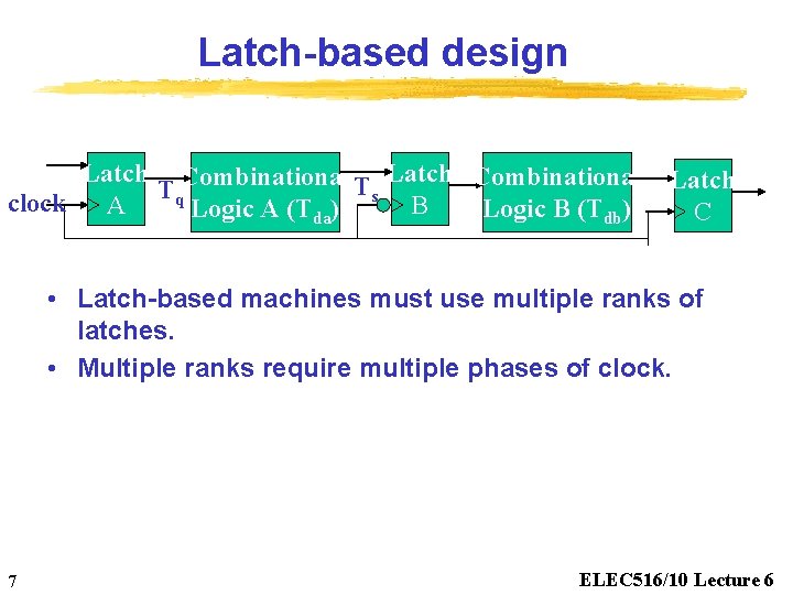
Latch-based design Latch Combinational Tq s clock A B Logic A (Tda) Logic B (Tdb) Latch C • Latch-based machines must use multiple ranks of latches. • Multiple ranks require multiple phases of clock. 7 ELEC 516/10 Lecture 6

Clock Race • In a synchronous system, if the data input to a register does not obey the setup and hold-time constraints, then potential clock race problems may occur. • Clock race results in erroneous data being stored in registers. • Assuming a perfectly synchronous system with perfect clocks, zero hold-time registers, and clock-to -Q time greater than the setup time, no clock race problem should occur. • However, at the chip level this might be hard to ensure. 8 ELEC 516/10 Lecture 6

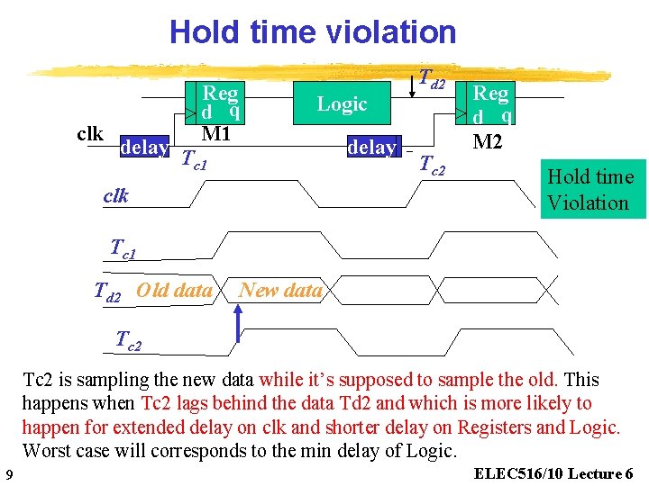
Hold time violation clk delay Reg d q M 1 Logic Tc 1 clk delay Td 2 Tc 2 Reg d q M 2 Hold time Violation Tc 1 Td 2 Old data New data Tc 2 is sampling the new data while it’s supposed to sample the old. This happens when Tc 2 lags behind the data Td 2 and which is more likely to happen for extended delay on clk and shorter delay on Registers and Logic. Worst case will corresponds to the min delay of Logic. 9 ELEC 516/10 Lecture 6

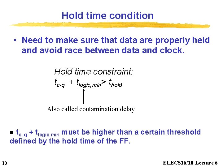
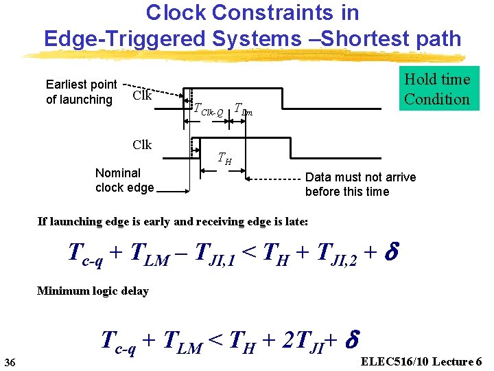
Hold time condition • Need to make sure that data are properly held and avoid race between data and clock. Hold time constraint: tc-q + tlogic, min> thold Also called contamination delay n tc_q + tlogic, min must be higher than a certain threshold defined by the hold time of the FF. 10 ELEC 516/10 Lecture 6

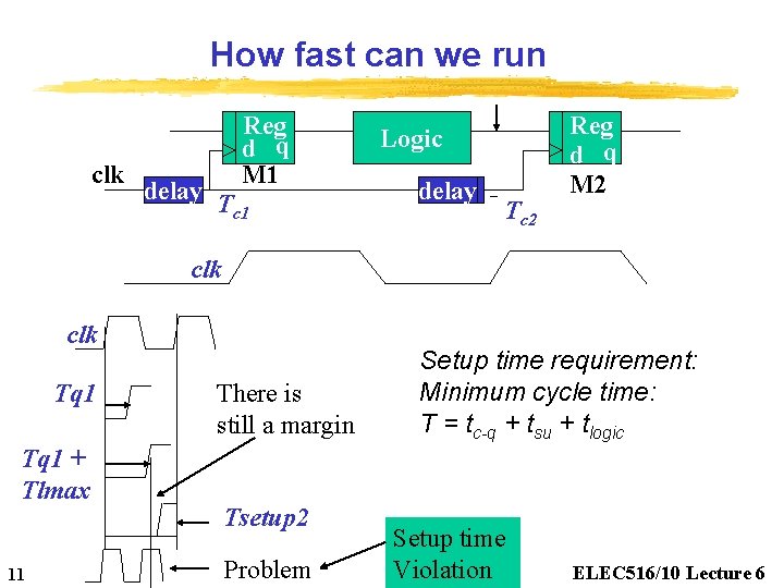
How fast can we run clk delay Reg d q M 1 Tc 1 Logic delay Tc 2 Reg d q M 2 clk Tq 1 + Tlmax 11 There is still a margin Tsetup 2 Problem Setup time requirement: Minimum cycle time: T = tc-q + tsu + tlogic Setup time Violation ELEC 516/10 Lecture 6

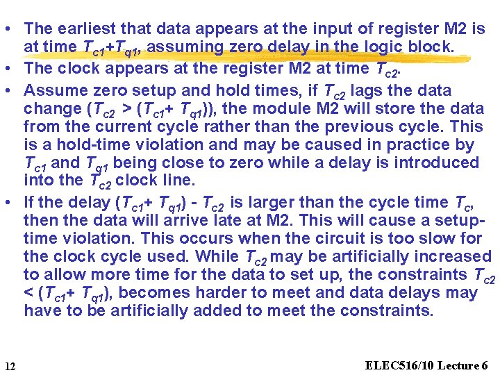
• The earliest that data appears at the input of register M 2 is at time Tc 1+Tq 1, assuming zero delay in the logic block. • The clock appears at the register M 2 at time Tc 2. • Assume zero setup and hold times, if Tc 2 lags the data change (Tc 2 > (Tc 1+ Tq 1)), the module M 2 will store the data from the current cycle rather than the previous cycle. This is a hold-time violation and may be caused in practice by Tc 1 and Tq 1 being close to zero while a delay is introduced into the Tc 2 clock line. • If the delay (Tc 1+ Tq 1) - Tc 2 is larger than the cycle time Tc, then the data will arrive late at M 2. This will cause a setuptime violation. This occurs when the circuit is too slow for the clock cycle used. While Tc 2 may be artificially increased to allow more time for the data to set up, the constraints Tc 2 < (Tc 1+ Tq 1), becomes harder to meet and data delays may have to be artificially added to meet the constraints. 12 ELEC 516/10 Lecture 6

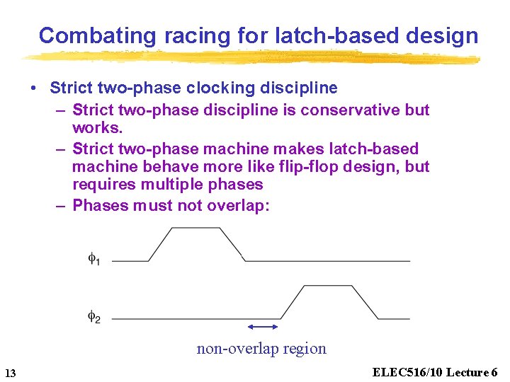
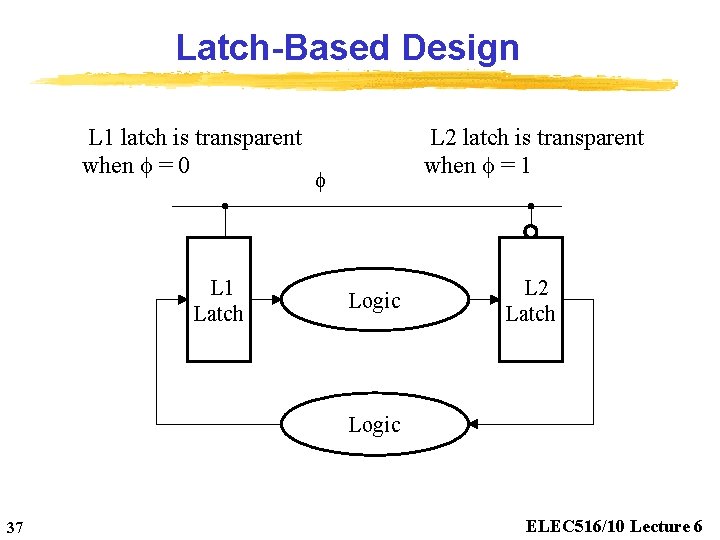
Combating racing for latch-based design • Strict two-phase clocking discipline – Strict two-phase discipline is conservative but works. – Strict two-phase machine makes latch-based machine behave more like flip-flop design, but requires multiple phases – Phases must not overlap: non-overlap region 13 ELEC 516/10 Lecture 6

Two phase clocking • Each phase has a one-sided constraint: phase must be long enough for all combinational delays. • If there are no combinational loops, phases can always be stretched to make that section of the machine work. • Total clock period depends on sum of phase periods. 14 ELEC 516/10 Lecture 6

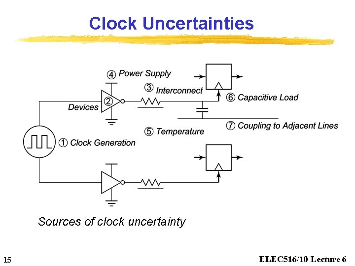
Clock Uncertainties Sources of clock uncertainty 15 ELEC 516/10 Lecture 6

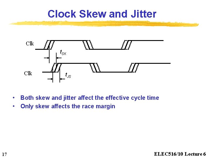
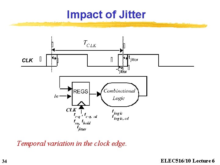
Clock Nonidealities • Clock skew – Spatial variation in temporally equivalent clock edges; deterministic + random, t. SK • Clock jitter – Temporal variations in consecutive edges of the clock signal; modulation + random noise – Cycle-to-cycle (short-term) t. JS – Long term t. JL • Variation of the pulse width – Important for level sensitive clocking 16 ELEC 516/10 Lecture 6

Clock Skew and Jitter Clk t. SK Clk t. JS • Both skew and jitter affect the effective cycle time • Only skew affects the race margin 17 ELEC 516/10 Lecture 6

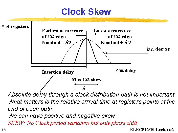
Clock Skew # of registers Earliest occurrence of Clk edge Nominal – /2 Latest occurrence of Clk edge Nominal + /2 Bad design Insertion delay Max Clk skew Clk delay Absolute delay through a clock distribution path is not important. What matters is the relative arrival time at registers points at the end of each path. We can have positive and negative skew SKEW: No Clock period variation but only phase shift 18 ELEC 516/10 Lecture 6

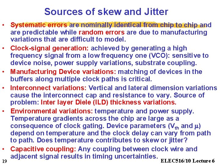
Sources of skew and Jitter • Systematic errors are nominally identical from chip to chip and are predictable while random errors are due to manufacturing variations that are difficult to model. • Clock-signal generation: achieved by generating a high frequency signal from a low frequency one (VCO): sensitive to device noise, power supply variations, substrate coupling. • Manufacturing Device variations: matching of devices in the buffers along multiple clock paths is critical. • Interconnect variations: Vertical and lateral dimension variations cause the interconnect cap and resistance to vary. Source of problem: Inter layer Diele (ILD) thickness variations. • Environmental variations: temperature and power supply. Temperature gradients across the chip are large as a consequence of clock gating. Device parameters (Vth and m) depend on temperature and the clock delay can vary from path to path. Does temperature contributes to skew or jitter? • Capacitive coupling: Any coupling between clock wire and adjacent signal results in timing uncertainties. 19 ELEC 516/10 Lecture 6

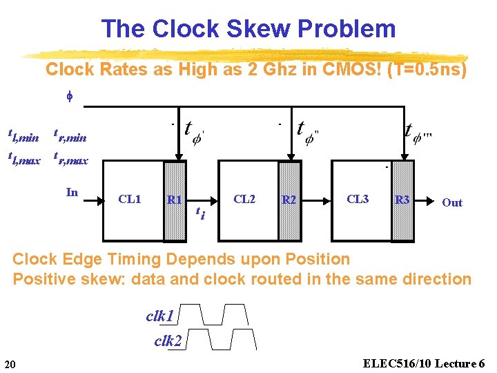
The Clock Skew Problem Clock Rates as High as 2 Ghz in CMOS! (T=0. 5 ns) f t l, min t r, min t l, max t r, max In CL 1 R 1 ti CL 2 R 2 CL 3 R 3 Out Clock Edge Timing Depends upon Positive skew: data and clock routed in the same direction clk 1 clk 2 20 ELEC 516/10 Lecture 6

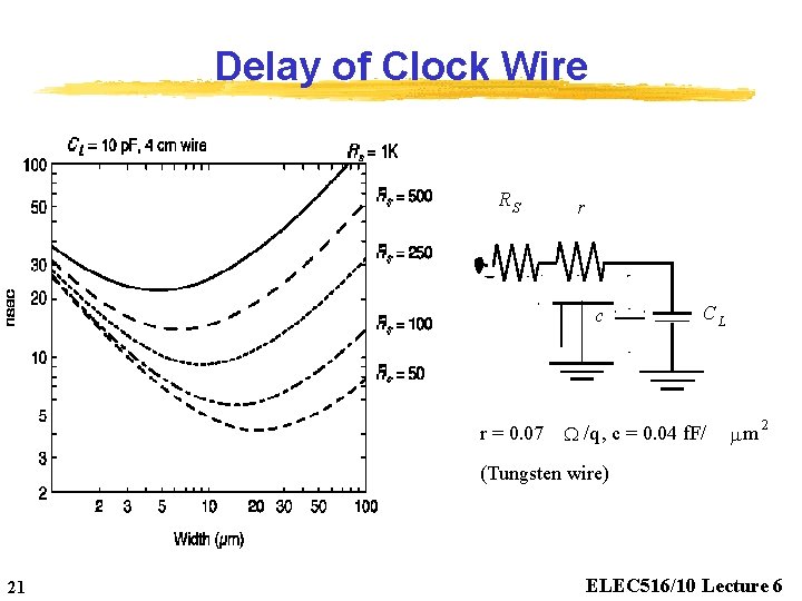
Delay of Clock Wire RS r c r = 0. 07 CL W /q , c = 0. 04 f. F/ mm 2 (Tungsten wire) 21 ELEC 516/10 Lecture 6

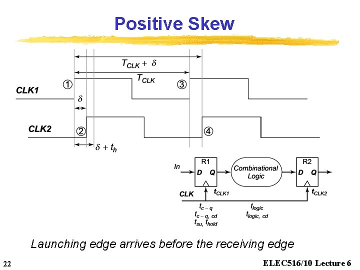
Positive Skew Launching edge arrives before the receiving edge 22 ELEC 516/10 Lecture 6

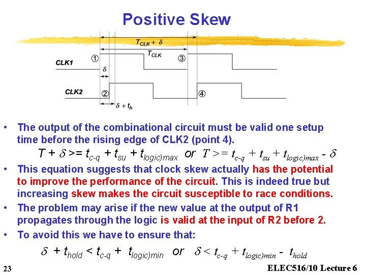
Positive Skew • The output of the combinational circuit must be valid one setup time before the rising edge of CLK 2 (point 4). T + >= tc-q + tsu + tlogic)max or T >= tc-q + tsu + tlogic)max - • This equation suggests that clock skew actually has the potential to improve the performance of the circuit. This is indeed true but increasing skew makes the circuit susceptible to race conditions. • The problem may arise if the new value at the output of R 1 propagates through the logic is valid at the input of R 2 before 2. • To avoid this we have to ensure that: + thold < tc-q + tlogic)min or < tc-q + tlogic)min - thold 23 ELEC 516/10 Lecture 6

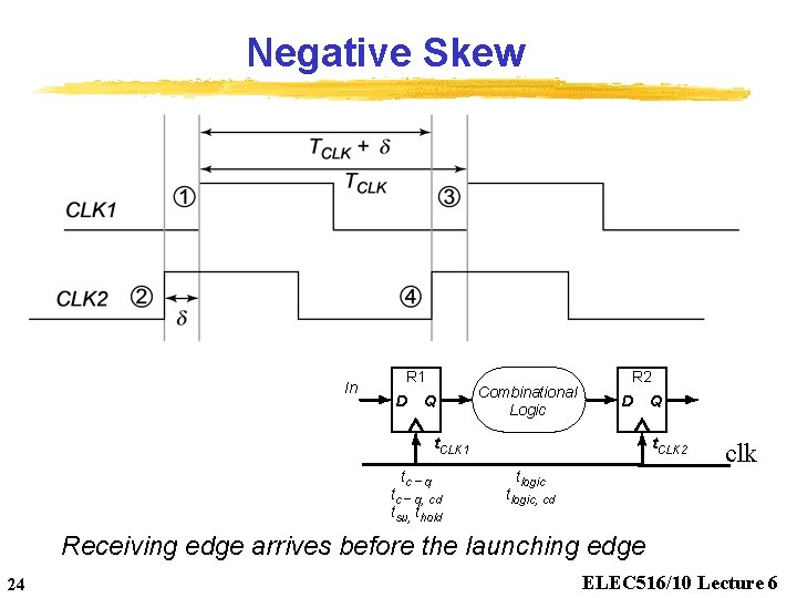
Negative Skew In R 1 D Q Combinational Logic R 2 D t. CLK 1 tc - q, cd tsu, thold Q t. CLK 2 clk tlogic, cd Receiving edge arrives before the launching edge 24 ELEC 516/10 Lecture 6

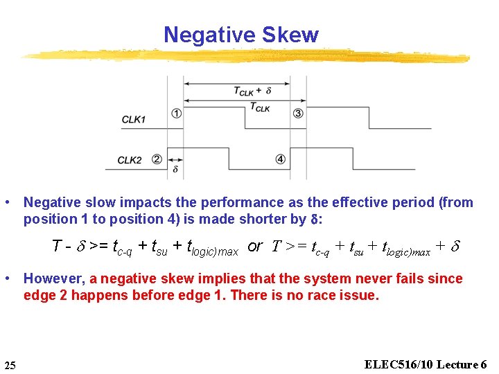
Negative Skew • Negative slow impacts the performance as the effective period (from position 1 to position 4) is made shorter by : T - >= tc-q + tsu + tlogic)max or T >= tc-q + tsu + tlogic)max + • However, a negative skew implies that the system never fails since edge 2 happens before edge 1. There is no race issue. 25 ELEC 516/10 Lecture 6

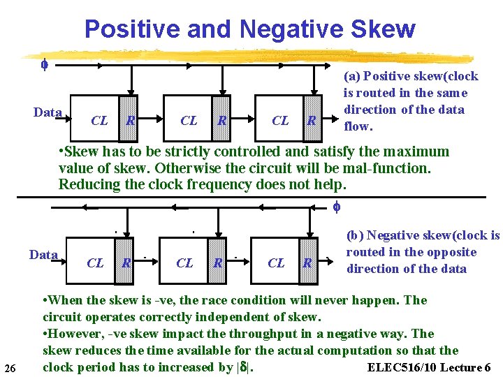
Positive and Negative Skew f Data CL R CL (a) Positive skew(clock is routed in the same direction of the data flow. R • Skew has to be strictly controlled and satisfy the maximum value of skew. Otherwise the circuit will be mal-function. Reducing the clock frequency does not help. f Data 26 CL R (b) Negative skew(clock is routed in the opposite direction of the data • When the skew is -ve, the race condition will never happen. The circuit operates correctly independent of skew. • However, -ve skew impact the throughput in a negative way. The skew reduces the time available for the actual computation so that the clock period has to increased by | |. ELEC 516/10 Lecture 6

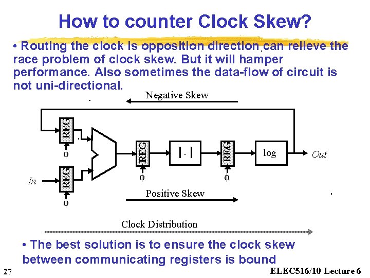
How to counter Clock Skew? • Routing the clock is opposition direction can relieve the race problem of clock skew. But it will hamper performance. Also sometimes the data-flow of circuit is not uni-directional. . REG In REG Negative Skew log Out Positive Skew Clock Distribution • The best solution is to ensure the clock skew between communicating registers is bound 27 ELEC 516/10 Lecture 6

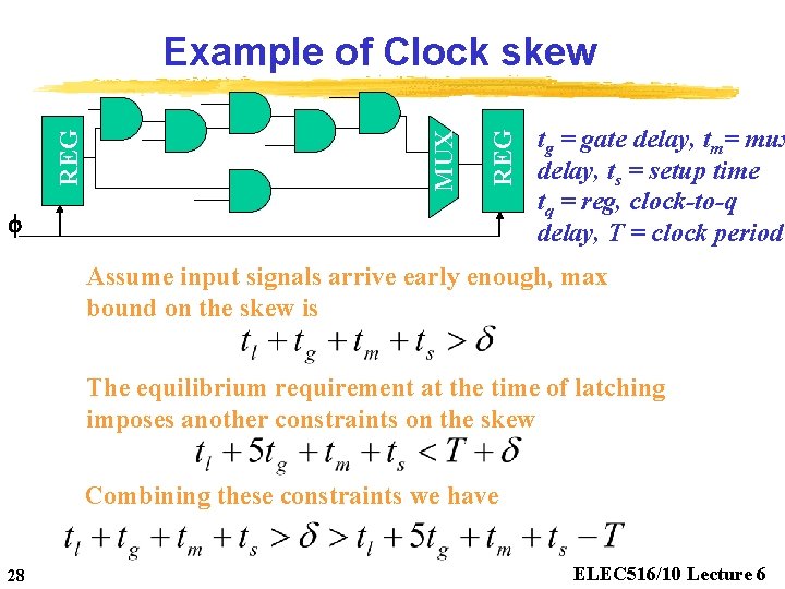
REG MUX REG Example of Clock skew f tg = gate delay, tm= mux delay, ts = setup time tq = reg, clock-to-q delay, T = clock period Assume input signals arrive early enough, max bound on the skew is The equilibrium requirement at the time of latching imposes another constraints on the skew Combining these constraints we have 28 ELEC 516/10 Lecture 6

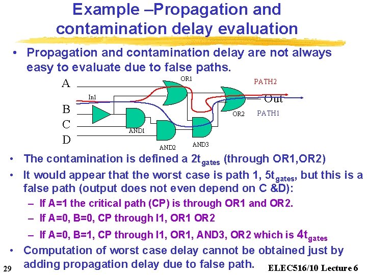
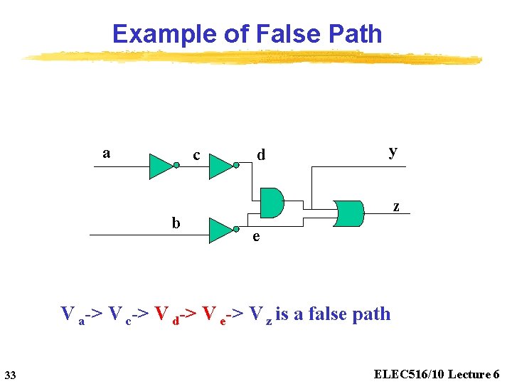
Example –Propagation and contamination delay evaluation • Propagation and contamination delay are not always easy to evaluate due to false paths. OR 1 PATH 2 A In 1 Out B PATH 1 OR 2 C AND 1 D AND 3 AND 2 REG • The contamination is defined a 2 tgates (through OR 1, OR 2) • It would appear that the worst case is path 1, 5 tgates, but this is a false path (output does not even depend on C &D): – If A=1 the critical path (CP) is through OR 1 and OR 2. – If A=0, B=0, CP through I 1, OR 1 OR 2 – If A=0, B=1, CP through I 1, OR 1, AND 3, OR 2 which is 4 tgates • Computation of worst case delay cannot be obtained just by ELEC 516/10 Lecture 6 29 adding propagation delay due to false path.

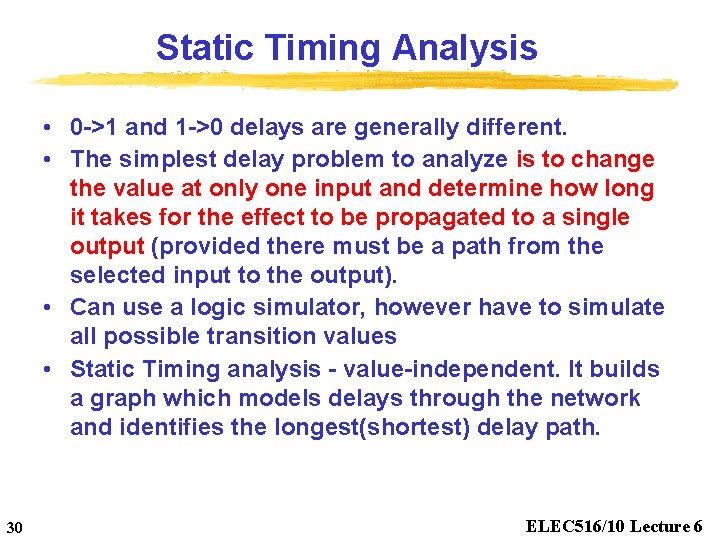
Static Timing Analysis • 0 ->1 and 1 ->0 delays are generally different. • The simplest delay problem to analyze is to change the value at only one input and determine how long it takes for the effect to be propagated to a single output (provided there must be a path from the selected input to the output). • Can use a logic simulator, however have to simulate all possible transition values • Static Timing analysis - value-independent. It builds a graph which models delays through the network and identifies the longest(shortest) delay path. 30 ELEC 516/10 Lecture 6

Critical Path • The longest delay path is known as critical path since that path limits the system performance. • The critical path not only tells us the system cycle time, it points out what part of the combinational logic must be changed to improved system performance. • Speed up gates on the critical path by increasing transistor sizes, or reducing wiring capacitance, or redesign logic along the critical path to use a faster gate configuration. • Speeding up the system may require modifying several sections of logic since the critical path can have multiple branches. Identify the critical path and identify the cutset of the graph represents the critical path. Then determine the edge (gate) to speed up. 31 ELEC 516/10 Lecture 6

False Path • False path - critical paths that can never be exercised during normal circuit operation. In this case the actual critical path is thus shorter than what would be predicted from the first-order analysis. • Detecting false path is not easy since it requires an understanding of the logic functionality of the network. • Also it is a N-P complete problem to determine whether a path is false or not, however new CAD tools/algorithm are available now to find false paths in practical networks. 32 ELEC 516/10 Lecture 6

Example of False Path a c b d y z e V a-> V c-> V d-> V e-> V z is a false path 33 ELEC 516/10 Lecture 6

Impact of Jitter Temporal variation in the clock edge. 34 ELEC 516/10 Lecture 6

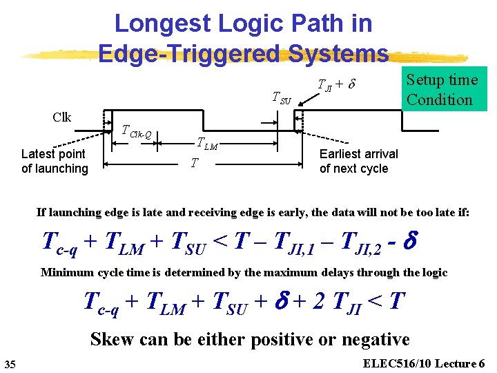
Longest Logic Path in Edge-Triggered Systems TSU Clk TClk-Q Latest point of launching TLM T Setup time Condition TJI + Earliest arrival of next cycle If launching edge is late and receiving edge is early, the data will not be too late if: Tc-q + TLM + TSU < T – TJI, 1 – TJI, 2 - Minimum cycle time is determined by the maximum delays through the logic Tc-q + TLM + TSU + + 2 TJI < T Skew can be either positive or negative 35 ELEC 516/10 Lecture 6

Clock Constraints in Edge-Triggered Systems –Shortest path Earliest point of launching Clk Nominal clock edge Hold time Condition TClk-Q TLm TH Data must not arrive before this time If launching edge is early and receiving edge is late: Tc-q + TLM – TJI, 1 < TH + TJI, 2 + Minimum logic delay 36 Tc-q + TLM < TH + 2 TJI+ ELEC 516/10 Lecture 6

Latch-Based Design L 1 latch is transparent when = 0 L 1 Latch L 2 latch is transparent when = 1 Logic L 2 Latch Logic 37 ELEC 516/10 Lecture 6

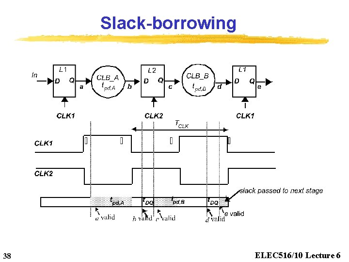
Slack-borrowing 38 ELEC 516/10 Lecture 6

Clock-distribution network design parameters • Interconnect material used for the clock network • Shape of the clock-distribution network • Clock driver and the buffer scheme used • Load on the clock lines (I. e. the clock fan-out) • Rise and fall time of the clock 39 ELEC 516/10 Lecture 6

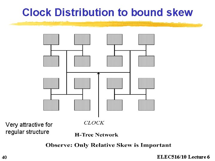
Clock Distribution to bound skew Very attractive for regular structure 40 ELEC 516/10 Lecture 6

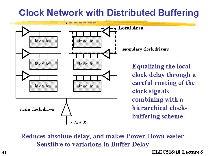
Clock Network with Distributed Buffering Local Area Module secondary clock drivers Module main clock driver Equalizing the local clock delay through a careful routing of the clock signals combining with a hierarchical clockbuffering scheme CLOCK Reduces absolute delay, and makes Power-Down easier Sensitive to variations in Buffer Delay 41 ELEC 516/10 Lecture 6
![More realistic Htree Restle 98 42 ELEC 51610 Lecture 6 More realistic H-tree [Restle 98] 42 ELEC 516/10 Lecture 6](https://slidetodoc.com/presentation_image_h/7937443dfa0ffc2895e125d336ef0aef/image-42.jpg)
More realistic H-tree [Restle 98] 42 ELEC 516/10 Lecture 6

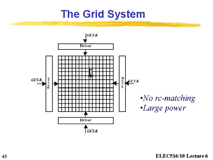
The Grid System • No rc-matching • Large power 43 ELEC 516/10 Lecture 6

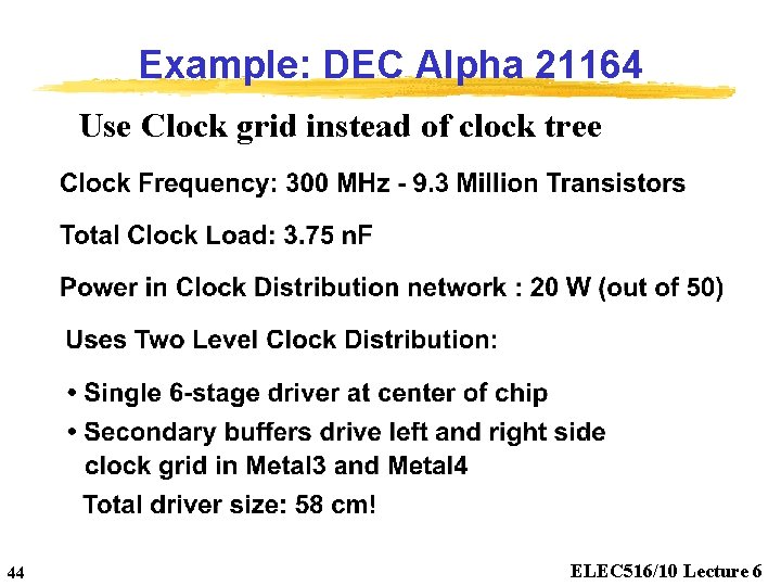
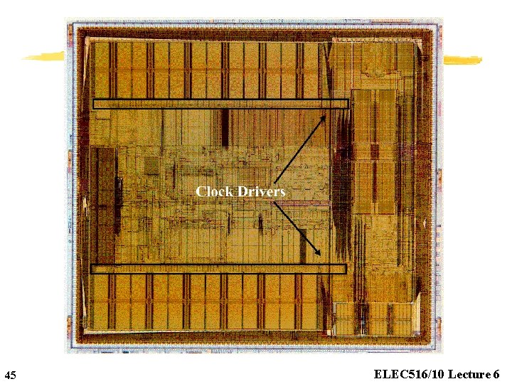
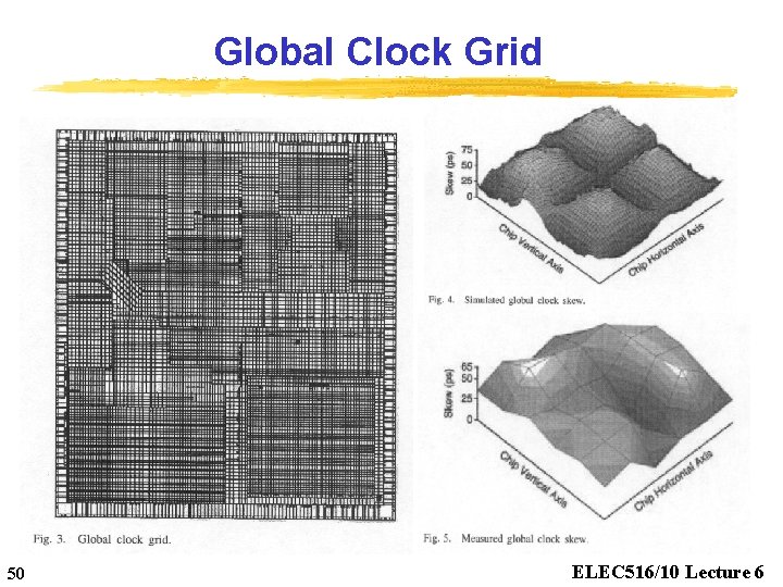
Example: DEC Alpha 21164 Use Clock grid instead of clock tree 44 ELEC 516/10 Lecture 6

45 ELEC 516/10 Lecture 6

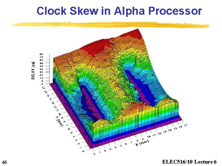
Clock Skew in Alpha Processor 46 ELEC 516/10 Lecture 6

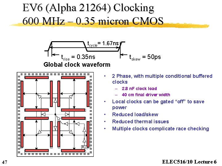
EV 6 (Alpha 21264) Clocking 600 MHz – 0. 35 micron CMOS tcycle= 1. 67 ns trise = 0. 35 ns Global clock waveform • tskew = 50 ps 2 Phase, with multiple conditional buffered clocks – 2. 8 n. F clock load – 40 cm final driver width • • 47 Local clocks can be gated “off” to save power Reduced load/skew Reduced thermal issues Multiple clocks complicate race checking ELEC 516/10 Lecture 6

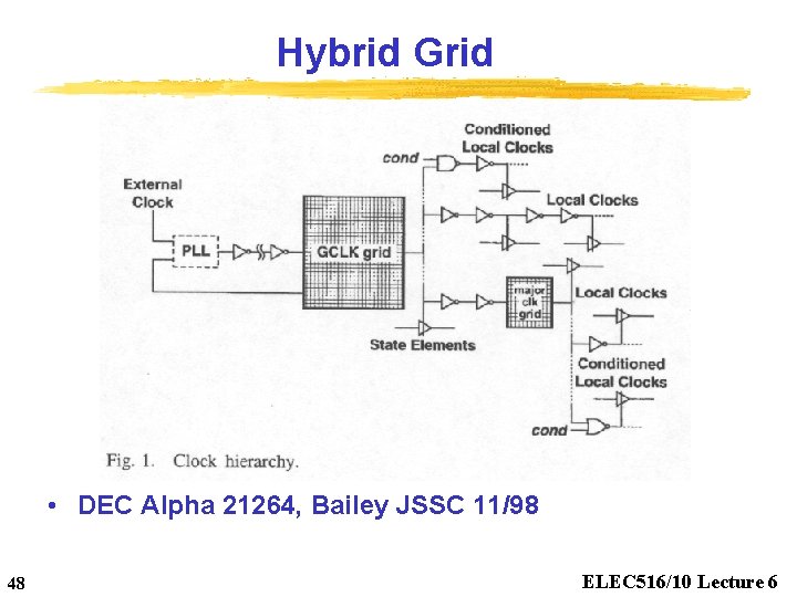
Hybrid Grid • DEC Alpha 21264, Bailey JSSC 11/98 48 ELEC 516/10 Lecture 6

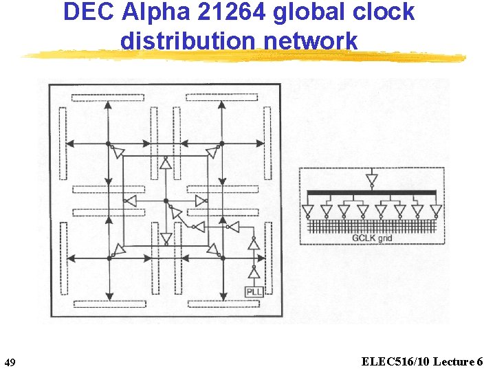
DEC Alpha 21264 global clock distribution network 49 ELEC 516/10 Lecture 6

Global Clock Grid 50 ELEC 516/10 Lecture 6

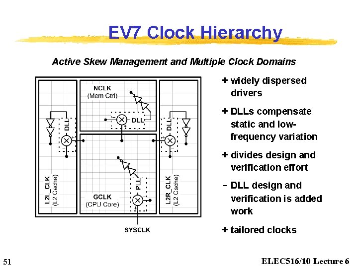
EV 7 Clock Hierarchy Active Skew Management and Multiple Clock Domains + widely dispersed drivers + DLLs compensate static and lowfrequency variation + divides design and verification effort - DLL design and verification is added work + tailored clocks 51 ELEC 516/10 Lecture 6

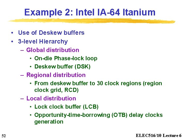
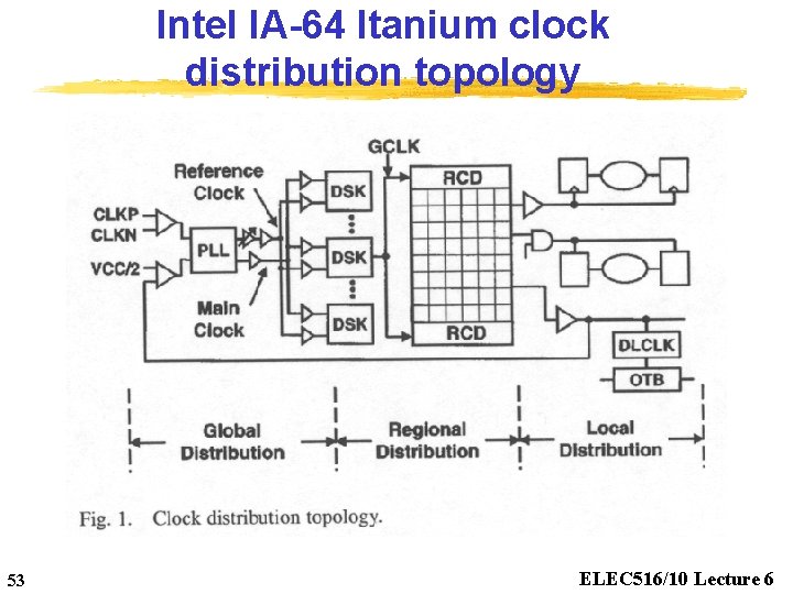
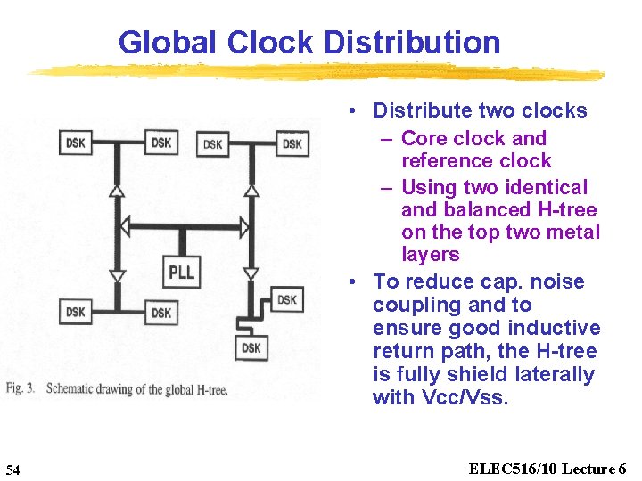
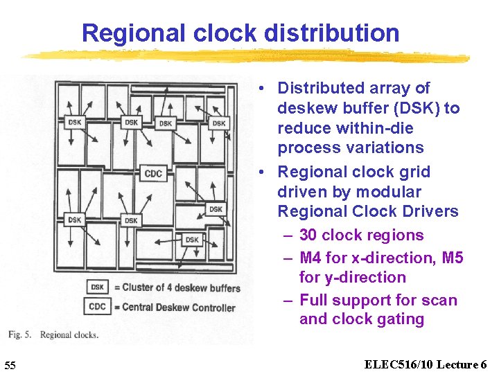
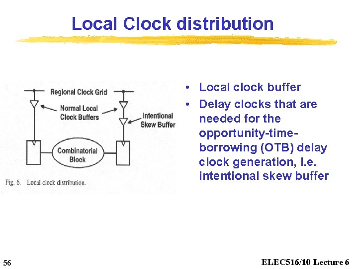
Example 2: Intel IA-64 Itanium • Use of Deskew buffers • 3 -level Hierarchy – Global distribution • On-die Phase-lock loop • Deskew buffer (DSK) – Regional distribution • From deskew buffer to 30 clock regions (region clock grid, RCD) – Local distribution • Lock clock buffer (LCB) • Opportunity-time-borrowing (OTB) delay clocks generation 52 ELEC 516/10 Lecture 6

Intel IA-64 Itanium clock distribution topology 53 ELEC 516/10 Lecture 6

Global Clock Distribution • Distribute two clocks – Core clock and reference clock – Using two identical and balanced H-tree on the top two metal layers • To reduce cap. noise coupling and to ensure good inductive return path, the H-tree is fully shield laterally with Vcc/Vss. 54 ELEC 516/10 Lecture 6

Regional clock distribution • Distributed array of deskew buffer (DSK) to reduce within-die process variations • Regional clock grid driven by modular Regional Clock Drivers – 30 clock regions – M 4 for x-direction, M 5 for y-direction – Full support for scan and clock gating 55 ELEC 516/10 Lecture 6

Local Clock distribution • Local clock buffer • Delay clocks that are needed for the opportunity-timeborrowing (OTB) delay clock generation, I. e. intentional skew buffer 56 ELEC 516/10 Lecture 6