CMOS Digital Integrated Circuits Chapter 10 Semiconductor Memories
- Slides: 79

CMOS Digital Integrated Circuits Chapter 10 Semiconductor Memories S. M. Kang, Y. Leblebici, and C. Kim 1 Copyright © 2014 Mc. Graw-Hill Education. Permission required for reproduction or display.

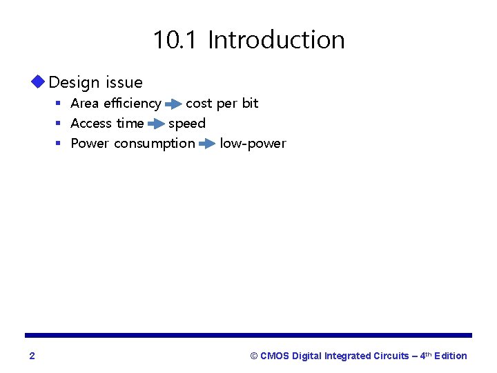
10. 1 Introduction u Design issue § Area efficiency cost per bit § Access time speed § Power consumption low-power 2 © CMOS Digital Integrated Circuits – 4 th Edition

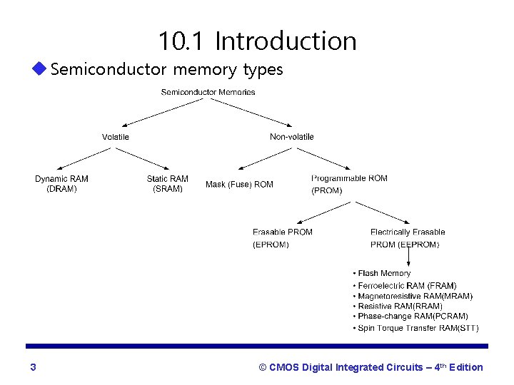
10. 1 Introduction u Semiconductor memory types 3 © CMOS Digital Integrated Circuits – 4 th Edition

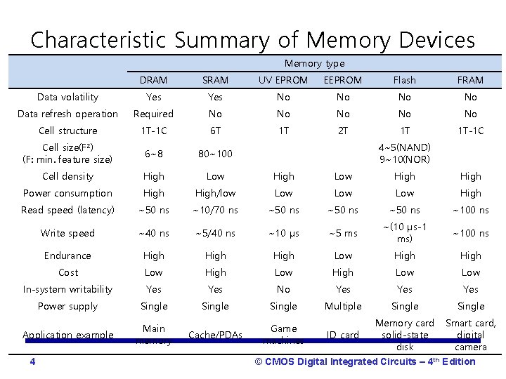
Characteristic Summary of Memory Devices Memory type DRAM SRAM UV EPROM EEPROM Flash FRAM Data volatility Yes No No Data refresh operation Required No No No Cell structure 1 T-1 C 6 T 1 T 2 T 1 T 1 T-1 C Cell size(F 2) (F: min. feature size) 6~8 80~100 Cell density High Low High Power consumption High/low Low Low High Read speed (latency) ~50 ns ~10/70 ns ~50 ns ~100 ns Write speed ~40 ns ~5/40 ns ~10 μs ~5 ms ~(10 μs-1 ms) ~100 ns Endurance High Low High Cost Low High Low In-system writability Yes No Yes Yes Power supply Single Multiple Single Application example Main memory Cache/PDAs Game machines ID card Memory card solid-state disk Smart card, digital camera 4 4~5(NAND) 9~10(NOR) © CMOS Digital Integrated Circuits – 4 th Edition

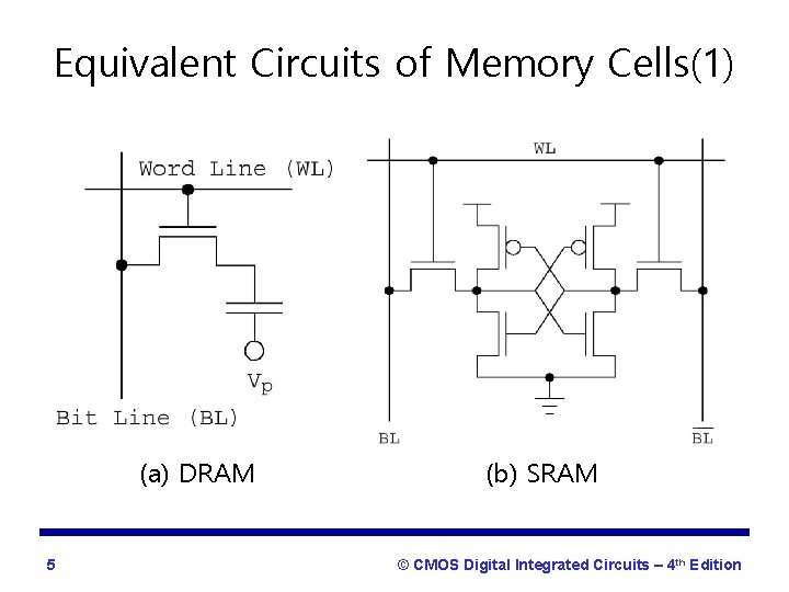
Equivalent Circuits of Memory Cells(1) (a) DRAM 5 (b) SRAM © CMOS Digital Integrated Circuits – 4 th Edition

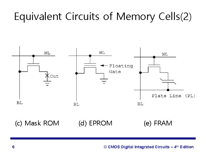
Equivalent Circuits of Memory Cells(2) (c) Mask ROM 6 (d) EPROM (e) FRAM © CMOS Digital Integrated Circuits – 4 th Edition

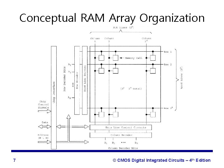
Conceptual RAM Array Organization 7 © CMOS Digital Integrated Circuits – 4 th Edition

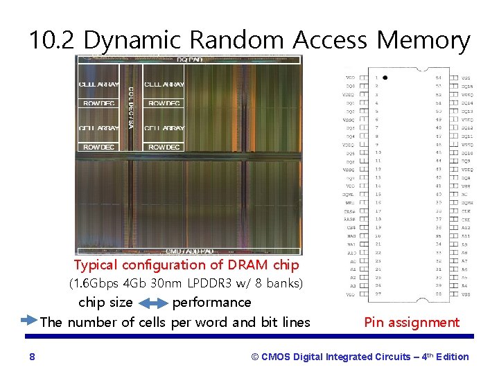
10. 2 Dynamic Random Access Memory Typical configuration of DRAM chip (1. 6 Gbps 4 Gb 30 nm LPDDR 3 w/ 8 banks) chip size performance The number of cells per word and bit lines 8 Pin assignment © CMOS Digital Integrated Circuits – 4 th Edition

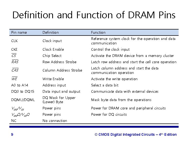
Definition and Function of DRAM Pins Pin name Definition Function CLK Clock input Reference system clock for the operation and data communication CKE Clock Enable Control the clock input CS Chip Select Activate the DRAM device from a memory cluster RAS Row Address Strobe Latch row address and start the cell core operation CAS Column Address Strobe Latch column address and start the data communication operation WE Write Enable Activate the write operation A 0 to A 14 Address input Select a data bit DQ 0 to DQ 15 Data input and output Communicate data with external devices DQMU/DQML DQ Mask for Upper (Lower) Byte Mask byte data from the operations VDD/VSS Power pins Power for DRAM core and peripheral circuits VDDQ/VSSQ Power pins Power for DQ circuits NC No connection 9 © CMOS Digital Integrated Circuits – 4 th Edition

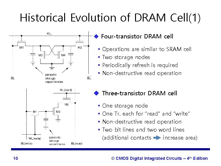
Historical Evolution of DRAM Cell(1) u Four-transistor DRAM cell § § Operations are similar to SRAM cell Two storage nodes Periodically refresh is required Non-destructive read operation u Three-transistor DRAM cell § § 10 One storage node One Tr. each for “read” and “write” Non-destructive read operation Two bit lines and two word lines (additional contacts increase area) © CMOS Digital Integrated Circuits – 4 th Edition

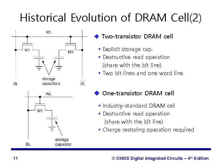
Historical Evolution of DRAM Cell(2) u Two-transistor DRAM cell § Explicit storage cap. § Destructive read operation (share with the bit line) § Two bit lines and one word line u One-transistor DRAM cell § Industry-standard DRAM cell § Destructive read operation (share with the bit line) § Charge restoring operation required 11 © CMOS Digital Integrated Circuits – 4 th Edition

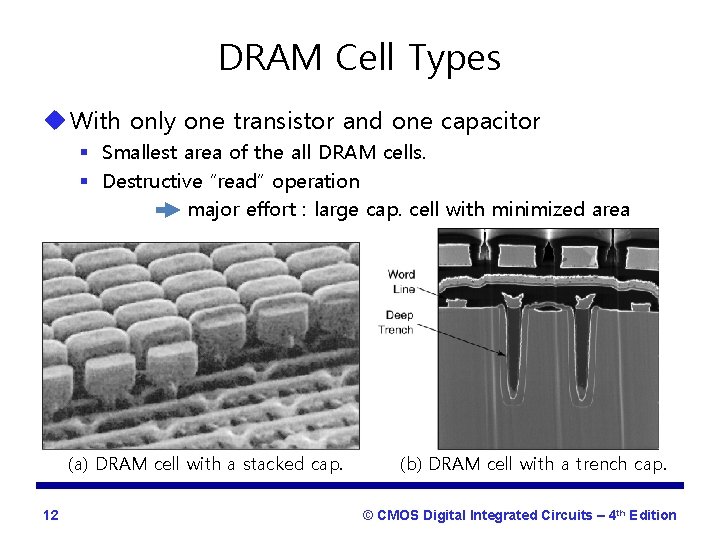
DRAM Cell Types u With only one transistor and one capacitor § Smallest area of the all DRAM cells. § Destructive “read” operation major effort : large cap. cell with minimized area (a) DRAM cell with a stacked cap. 12 (b) DRAM cell with a trench cap. © CMOS Digital Integrated Circuits – 4 th Edition

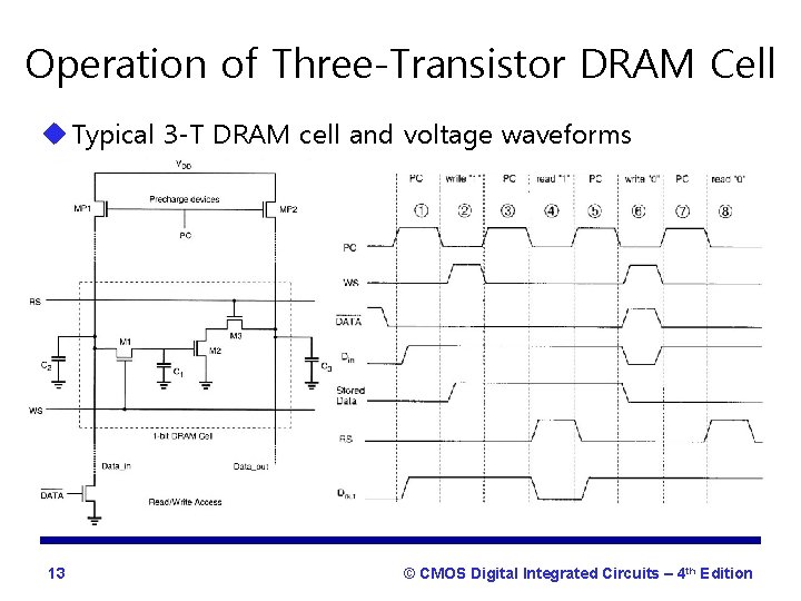
Operation of Three-Transistor DRAM Cell u Typical 3 -T DRAM cell and voltage waveforms 13 © CMOS Digital Integrated Circuits – 4 th Edition

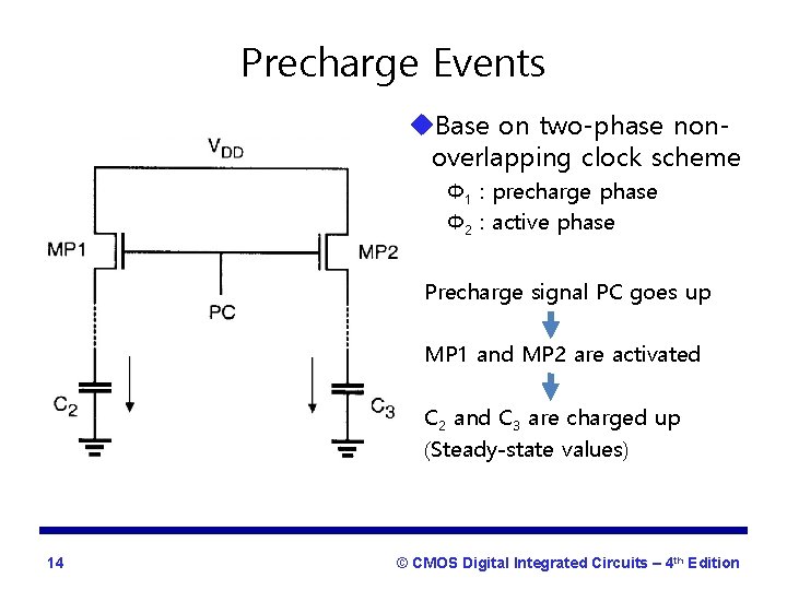
Precharge Events u. Base on two-phase nonoverlapping clock scheme Φ 1 : precharge phase Φ 2 : active phase Precharge signal PC goes up MP 1 and MP 2 are activated C 2 and C 3 are charged up (Steady-state values) 14 © CMOS Digital Integrated Circuits – 4 th Edition

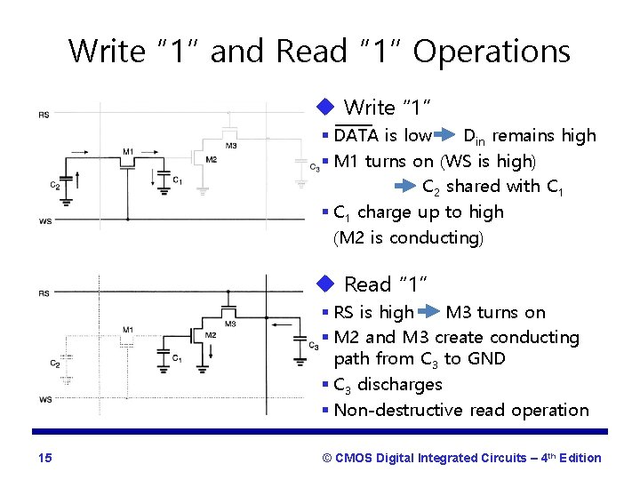
Write “ 1” and Read “ 1” Operations u Write “ 1” § DATA is low Din remains high § M 1 turns on (WS is high) C 2 shared with C 1 § C 1 charge up to high (M 2 is conducting) u Read “ 1” § RS is high M 3 turns on § M 2 and M 3 create conducting path from C 3 to GND § C 3 discharges § Non-destructive read operation 15 © CMOS Digital Integrated Circuits – 4 th Edition

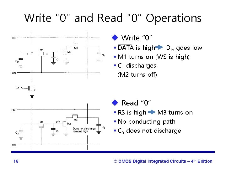
Write “ 0” and Read “ 0” Operations u Write “ 0” § DATA is high Din goes low § M 1 turns on (WS is high) § C 1 discharges (M 2 turns off) u Read “ 0” § RS is high M 3 turns on § No conducting path § C 3 does not discharge 16 © CMOS Digital Integrated Circuits – 4 th Edition

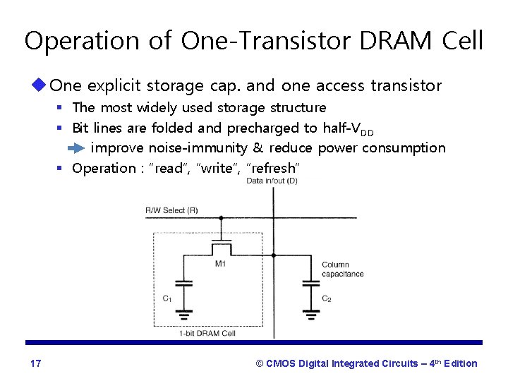
Operation of One-Transistor DRAM Cell u One explicit storage cap. and one access transistor § The most widely used storage structure § Bit lines are folded and precharged to half-VDD improve noise-immunity & reduce power consumption § Operation : “read”, “write”, “refresh” 17 © CMOS Digital Integrated Circuits – 4 th Edition

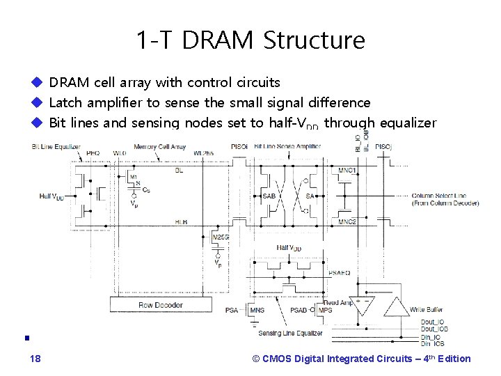
1 -T DRAM Structure u DRAM cell array with control circuits u Latch amplifier to sense the small signal difference u Bit lines and sensing nodes set to half-VDD through equalizer 18 © CMOS Digital Integrated Circuits – 4 th Edition

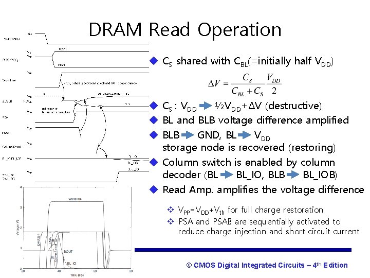
DRAM Read Operation u CS shared with CBL(=initially half VDD) u CS : VDD ½VDD+ΔV (destructive) u BL and BLB voltage difference amplified u BLB GND, BL VDD storage node is recovered (restoring) u Column switch is enabled by column decoder (BL BL_IO, BLB BL_IOB) u Read Amp. amplifies the voltage difference v VPP=VDD+Vth for full charge restoration v PSA and PSAB are sequentially activated to reduce charge injection and short circuit current 19 © CMOS Digital Integrated Circuits – 4 th Edition

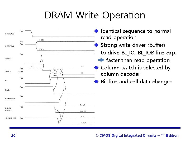
DRAM Write Operation u Identical sequence to normal read operation u Strong write driver (buffer) to drive BL_IO, BL_IOB line cap. faster than read operation u Column switch is selected by column decoder u Bit line and cell data changed 20 © CMOS Digital Integrated Circuits – 4 th Edition

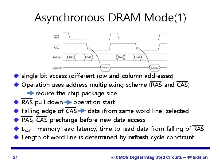
Asynchronous DRAM Mode(1) u single bit access (different row and column addresses) u Operation uses address multiplexing scheme (RAS and CAS) reduce the chip package size u RAS pull down operation start u Falling edge of CAS data (from same word line) selected u RAS, CAS precharge before new data access u t. RAC : memory read latency, time to read data from falling of RAS u Length of word line is determined by refresh cycle constraint 21 © CMOS Digital Integrated Circuits – 4 th Edition

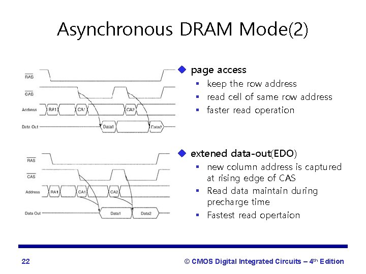
Asynchronous DRAM Mode(2) u page access § keep the row address § read cell of same row address § faster read operation u extened data-out(EDO) § new column address is captured at rising edge of CAS § Read data maintain during precharge time § Fastest read opertaion 22 © CMOS Digital Integrated Circuits – 4 th Edition

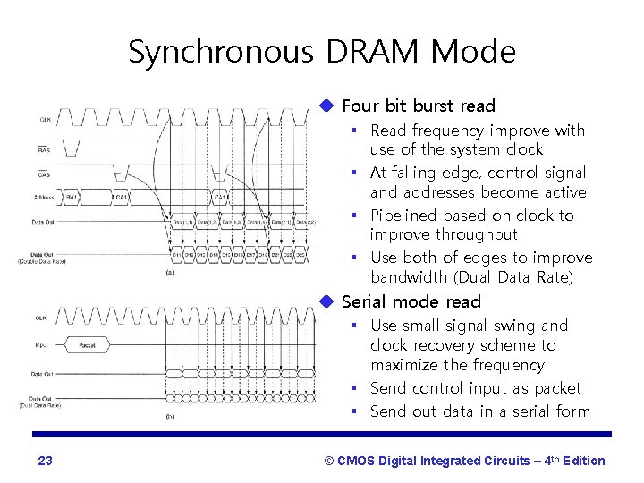
Synchronous DRAM Mode u Four bit burst read § Read frequency improve with use of the system clock § At falling edge, control signal and addresses become active § Pipelined based on clock to improve throughput § Use both of edges to improve bandwidth (Dual Data Rate) u Serial mode read § Use small signal swing and clock recovery scheme to maximize the frequency § Send control input as packet § Send out data in a serial form 23 © CMOS Digital Integrated Circuits – 4 th Edition

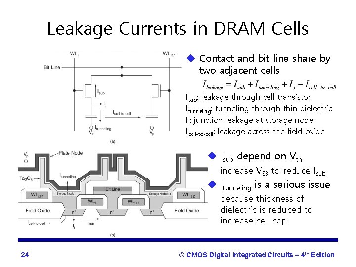
Leakage Currents in DRAM Cells u Contact and bit line share by two adjacent cells Isub: leakage through cell transistor Itunneling: tunneling through thin dielectric Ij: junction leakage at storage node Icell-to-cell: leakage across the field oxide u Isub depend on Vth increase VSB to reduce Isub u Itunneling is a serious issue because thickness of dielectric is reduced to increase cell cap. 24 © CMOS Digital Integrated Circuits – 4 th Edition

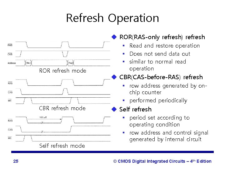
Refresh Operation u ROR(RAS-only refresh) refresh ROR refresh mode § Read and restore operation § Does not send data out § similar to normal read operation u CBR(CAS-before-RAS) refresh § row address generated by onchip counter § performed periodically CBR refresh mode Self refresh mode 25 u Self refresh § period set according to operating condition § row address and control signal generated by internal circuit © CMOS Digital Integrated Circuits – 4 th Edition

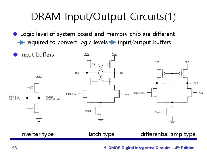
DRAM Input/Output Circuits(1) u Logic level of system board and memory chip are different required to convert logic levels input/output buffers u Input buffers inverter type 26 latch type differential amp type © CMOS Digital Integrated Circuits – 4 th Edition

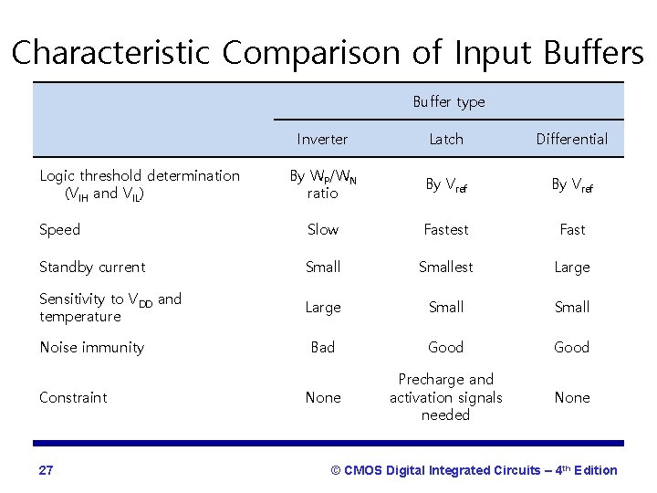
Characteristic Comparison of Input Buffers Buffer type Inverter Latch Differential By WP/WN ratio By Vref Speed Slow Fastest Fast Standby current Smallest Large Sensitivity to VDD and temperature Large Small Bad Good None Precharge and activation signals needed None Logic threshold determination (VIH and VIL) Noise immunity Constraint 27 © CMOS Digital Integrated Circuits – 4 th Edition

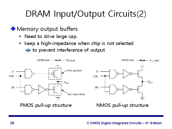
DRAM Input/Output Circuits(2) u Memory output buffers § Need to drive large cap. § Keep a high-impedance when chip is not selected to prevent interference of output PMOS pull-up structure 28 NMOS pull-up structure © CMOS Digital Integrated Circuits – 4 th Edition

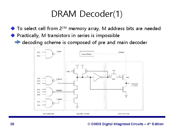
DRAM Decoder(1) u To select cell from 22 M memory array, M address bits are needed u Practically, M transistors in series is impossible decoding scheme is composed of pre and main decoder 29 © CMOS Digital Integrated Circuits – 4 th Edition

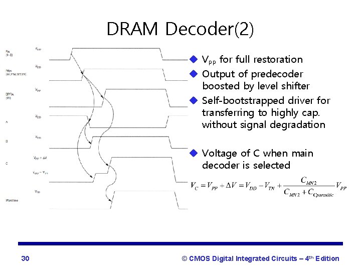
DRAM Decoder(2) u VPP for full restoration u Output of predecoder boosted by level shifter u Self-bootstrapped driver for transferring to highly cap. without signal degradation u Voltage of C when main decoder is selected 30 © CMOS Digital Integrated Circuits – 4 th Edition

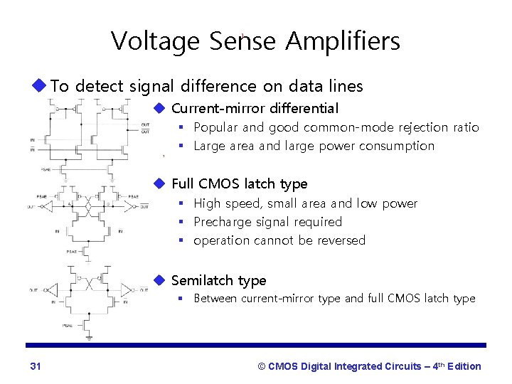
Voltage Sense Amplifiers u To detect signal difference on data lines u Current-mirror differential § Popular and good common-mode rejection ratio § Large area and large power consumption u Full CMOS latch type § High speed, small area and low power § Precharge signal required § operation cannot be reversed u Semilatch type § Between current-mirror type and full CMOS latch type 31 © CMOS Digital Integrated Circuits – 4 th Edition

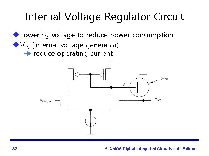
Internal Voltage Regulator Circuit u Lowering voltage to reduce power consumption u VINT(internal voltage generator) reduce operating current 32 © CMOS Digital Integrated Circuits – 4 th Edition

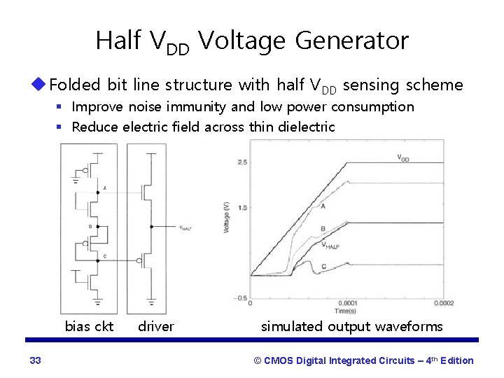
Half VDD Voltage Generator u Folded bit line structure with half VDD sensing scheme § Improve noise immunity and low power consumption § Reduce electric field across thin dielectric bias ckt 33 driver simulated output waveforms © CMOS Digital Integrated Circuits – 4 th Edition

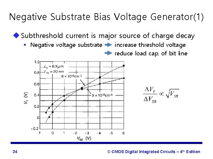
Negative Substrate Bias Voltage Generator(1) u Subthreshold current is major source of charge decay § Negative voltage substrate 34 increase threshold voltage reduce load cap. of bit line © CMOS Digital Integrated Circuits – 4 th Edition

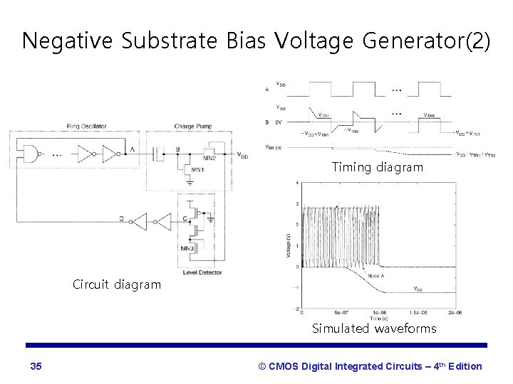
Negative Substrate Bias Voltage Generator(2) Timing diagram Circuit diagram Simulated waveforms 35 © CMOS Digital Integrated Circuits – 4 th Edition

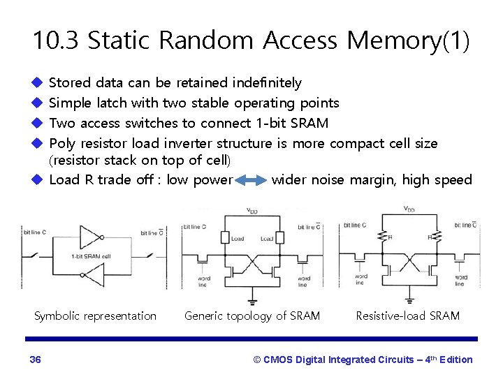
10. 3 Static Random Access Memory(1) Stored data can be retained indefinitely Simple latch with two stable operating points Two access switches to connect 1 -bit SRAM Poly resistor load inverter structure is more compact cell size (resistor stack on top of cell) u Load R trade off : low power wider noise margin, high speed u u Symbolic representation 36 Generic topology of SRAM Resistive-load SRAM © CMOS Digital Integrated Circuits – 4 th Edition

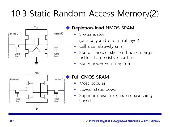
10. 3 Static Random Access Memory(2) u Depletion-load NMOS SRAM § Six-transistor (one poly and one metal layer) § Cell size relatively small § Static characteristics and noise margins better than resistive-load cell § Static power consumption u Full CMOS SRAM § Most popular § Lowest static power § Superior noise margins and switching speed 37 © CMOS Digital Integrated Circuits – 4 th Edition

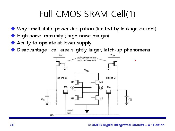
Full CMOS SRAM Cell(1) u u 38 Very small static power dissipation (limited by leakage current) High noise immunity (large noise margin) Ability to operate at lower supply Disadvantage : cell area slightly larger, latch-up phenomena © CMOS Digital Integrated Circuits – 4 th Edition

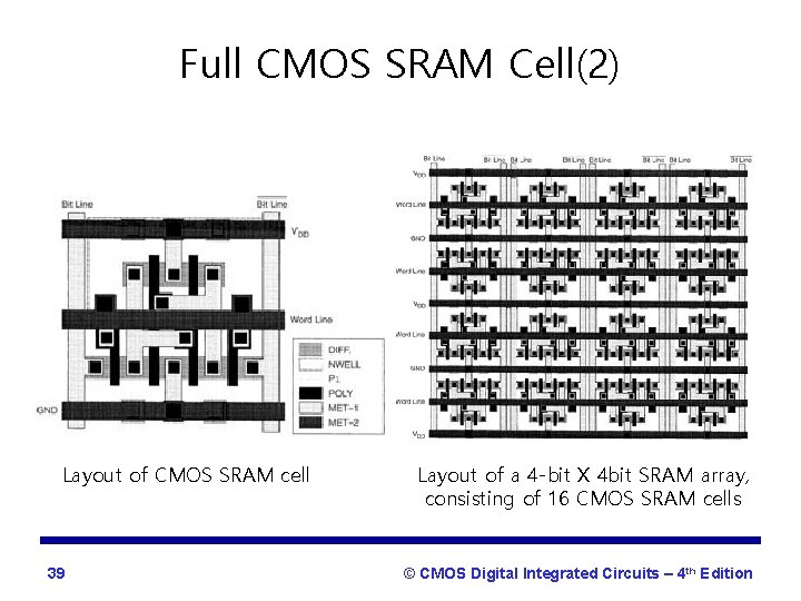
Full CMOS SRAM Cell(2) Layout of CMOS SRAM cell 39 Layout of a 4 -bit X 4 bit SRAM array, consisting of 16 CMOS SRAM cells © CMOS Digital Integrated Circuits – 4 th Edition

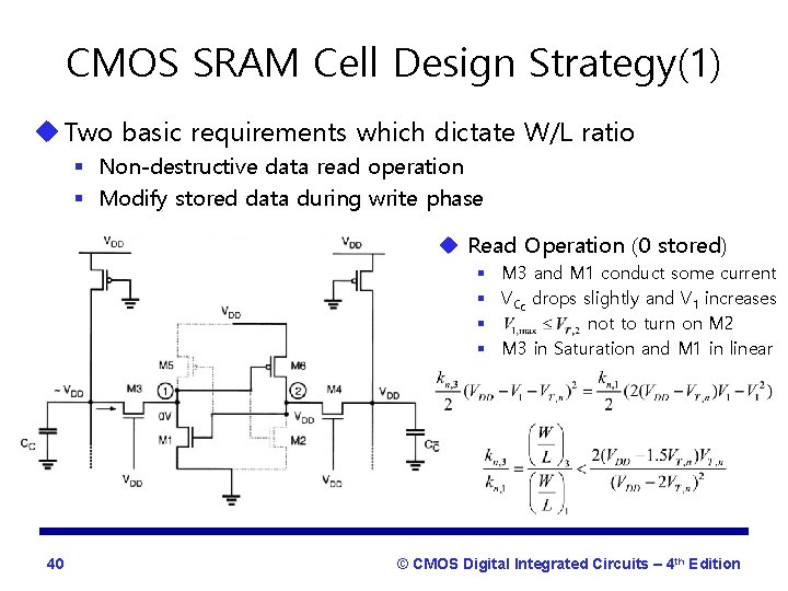
CMOS SRAM Cell Design Strategy(1) u Two basic requirements which dictate W/L ratio § Non-destructive data read operation § Modify stored data during write phase u Read Operation (0 stored) § M 3 and M 1 conduct some current § VCc drops slightly and V 1 increases § not to turn on M 2 § M 3 in Saturation and M 1 in linear 40 © CMOS Digital Integrated Circuits – 4 th Edition

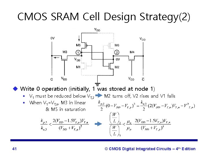
CMOS SRAM Cell Design Strategy(2) u Write 0 operation (initially, 1 was stored at node 1) § V 1 must be reduced below VT, 2 § When V 1=VT, n, M 3 in linear & M 5 in saturation 41 M 2 turns off, V 2 rises and V 1 falls © CMOS Digital Integrated Circuits – 4 th Edition

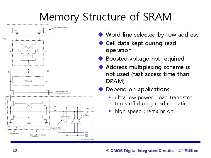
Memory Structure of SRAM u Word line selected by row address u Cell data kept during read operation u Boosted voltage not required u Address multiplexing scheme is not used (fast access time than DRAM) u Depend on applications § ultra low power : load transistor turns off during read operation § high speed : remains on 42 © CMOS Digital Integrated Circuits – 4 th Edition

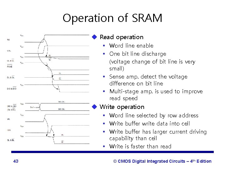
Operation of SRAM u Read operation § Word line enable § One bit line discharge (voltage change of bit line is very small) § Sense amp. detect the voltage difference on bit line § Multi-stage amp. is used to improve read speed u Write operation § Word line selected by row address § Write buffer write data into cell § Write buffer has larger current driving capability than cell § Write is faster than read 43 © CMOS Digital Integrated Circuits – 4 th Edition

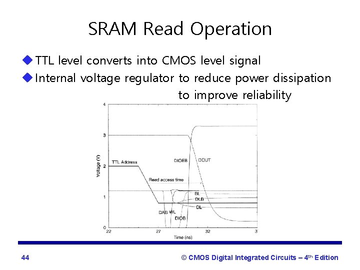
SRAM Read Operation u TTL level converts into CMOS level signal u Internal voltage regulator to reduce power dissipation to improve reliability 44 © CMOS Digital Integrated Circuits – 4 th Edition

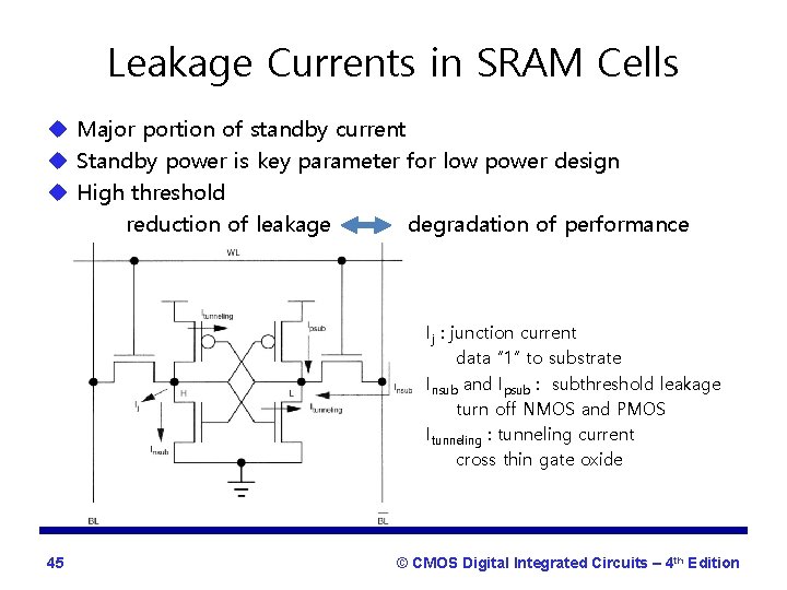
Leakage Currents in SRAM Cells u Major portion of standby current u Standby power is key parameter for low power design u High threshold reduction of leakage degradation of performance Ij : junction current data “ 1” to substrate Insub and Ipsub : subthreshold leakage turn off NMOS and PMOS Itunneling : tunneling current cross thin gate oxide 45 © CMOS Digital Integrated Circuits – 4 th Edition

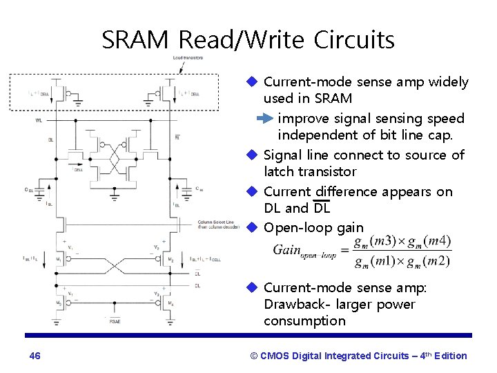
SRAM Read/Write Circuits u Current-mode sense amp widely used in SRAM improve signal sensing speed independent of bit line cap. u Signal line connect to source of latch transistor u Current difference appears on DL and DL u Open-loop gain u Current-mode sense amp: Drawback- larger power consumption 46 © CMOS Digital Integrated Circuits – 4 th Edition

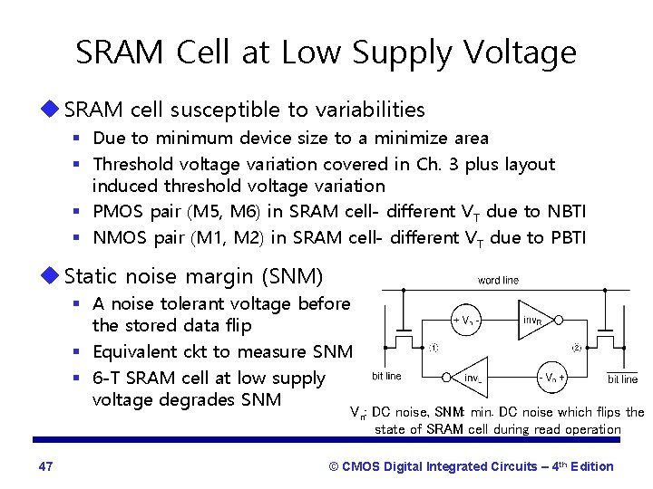
SRAM Cell at Low Supply Voltage u SRAM cell susceptible to variabilities § Due to minimum device size to a minimize area § Threshold voltage variation covered in Ch. 3 plus layout induced threshold voltage variation § PMOS pair (M 5, M 6) in SRAM cell- different VT due to NBTI § NMOS pair (M 1, M 2) in SRAM cell- different VT due to PBTI u Static noise margin (SNM) § A noise tolerant voltage before the stored data flip § Equivalent ckt to measure SNM § 6 -T SRAM cell at low supply voltage degrades SNM Vn: DC noise, SNM: min. DC noise which flips the state of SRAM cell during read operation 47 © CMOS Digital Integrated Circuits – 4 th Edition

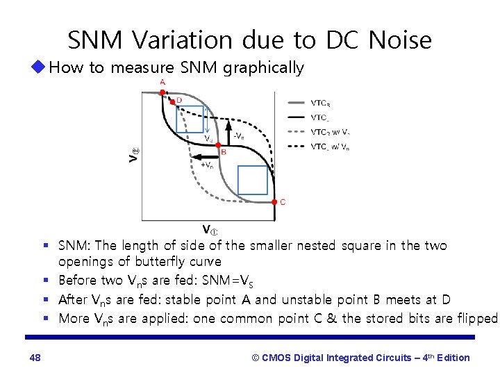
SNM Variation due to DC Noise u How to measure SNM graphically § SNM: The length of side of the smaller nested square in the two openings of butterfly curve § Before two Vns are fed: SNM=VS § After Vns are fed: stable point A and unstable point B meets at D § More Vns are applied: one common point C & the stored bits are flipped 48 © CMOS Digital Integrated Circuits – 4 th Edition

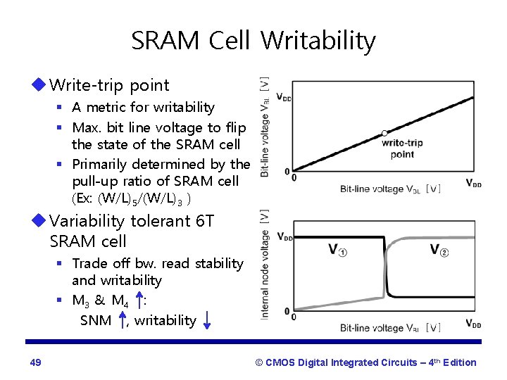
SRAM Cell Writability u Write-trip point § A metric for writability § Max. bit line voltage to flip the state of the SRAM cell § Primarily determined by the pull-up ratio of SRAM cell (Ex: (W/L)5/(W/L)3 ) u Variability tolerant 6 T SRAM cell § Trade off bw. read stability and writability § M 3 & M 4 : SNM , writability 49 © CMOS Digital Integrated Circuits – 4 th Edition

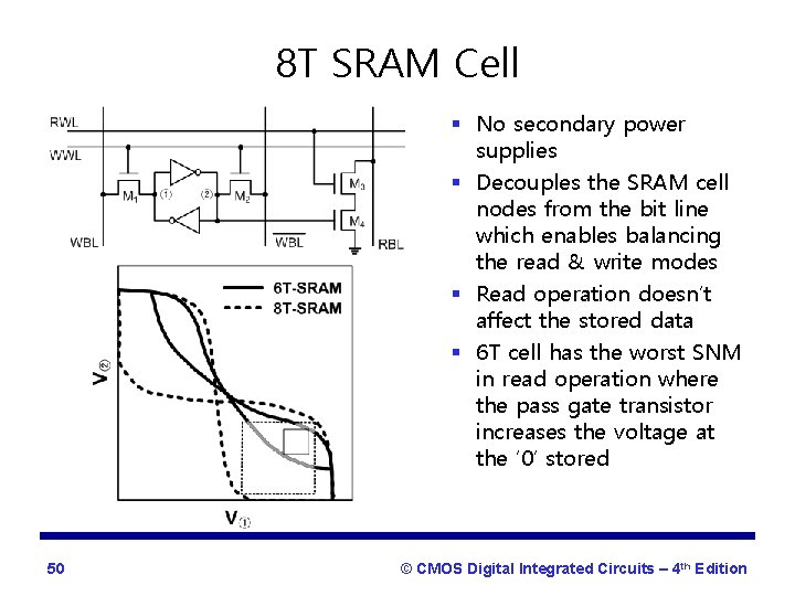
8 T SRAM Cell § No secondary power supplies § Decouples the SRAM cell nodes from the bit line which enables balancing the read & write modes § Read operation doesn’t affect the stored data § 6 T cell has the worst SNM in read operation where the pass gate transistor increases the voltage at the ‘ 0’ stored 50 © CMOS Digital Integrated Circuits – 4 th Edition

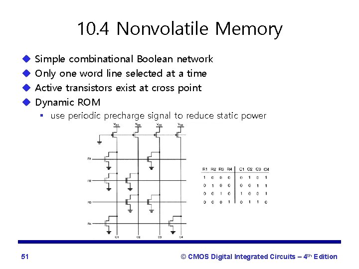
10. 4 Nonvolatile Memory u u Simple combinational Boolean network Only one word line selected at a time Active transistors exist at cross point Dynamic ROM § use periodic precharge signal to reduce static power 51 © CMOS Digital Integrated Circuits – 4 th Edition

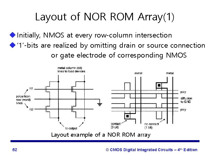
Layout of NOR ROM Array(1) u Initially, NMOS at every row-column intersection u ‘ 1’-bits are realized by omitting drain or source connection or gate electrode of corresponding NMOS Layout example of a NOR ROM array 52 © CMOS Digital Integrated Circuits – 4 th Edition

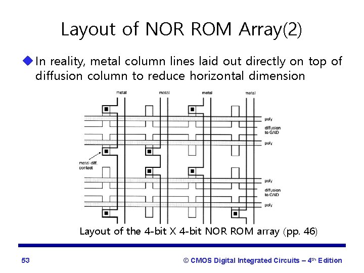
Layout of NOR ROM Array(2) u In reality, metal column lines laid out directly on top of diffusion column to reduce horizontal dimension Layout of the 4 -bit X 4 -bit NOR ROM array (pp. 46) 53 © CMOS Digital Integrated Circuits – 4 th Edition

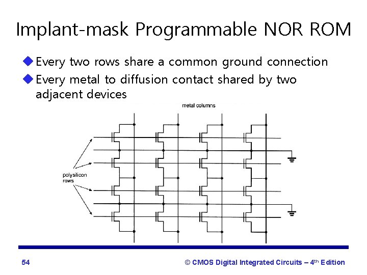
Implant-mask Programmable NOR ROM u Every two rows share a common ground connection u Every metal to diffusion contact shared by two adjacent devices 54 © CMOS Digital Integrated Circuits – 4 th Edition

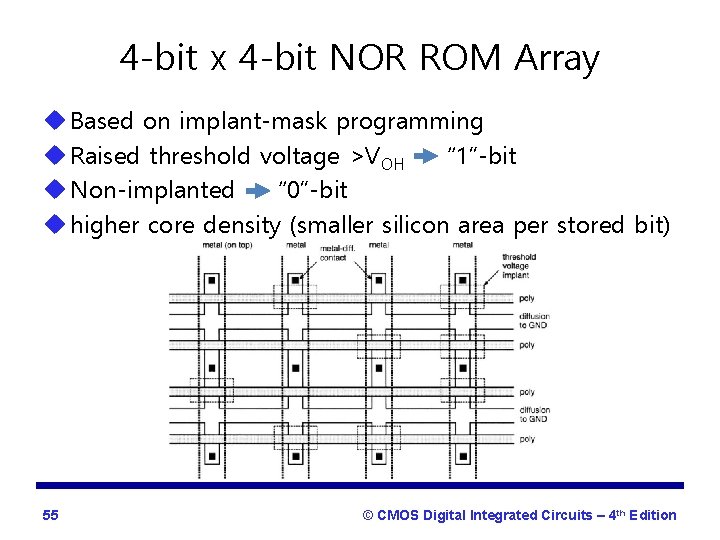
4 -bit x 4 -bit NOR ROM Array u Based on implant-mask programming u Raised threshold voltage >VOH “ 1”-bit u Non-implanted “ 0”-bit u higher core density (smaller silicon area per stored bit) 55 © CMOS Digital Integrated Circuits – 4 th Edition

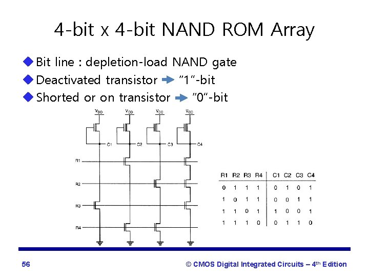
4 -bit x 4 -bit NAND ROM Array u Bit line : depletion-load NAND gate u Deactivated transistor “ 1”-bit u Shorted or on transistor “ 0”-bit 56 © CMOS Digital Integrated Circuits – 4 th Edition

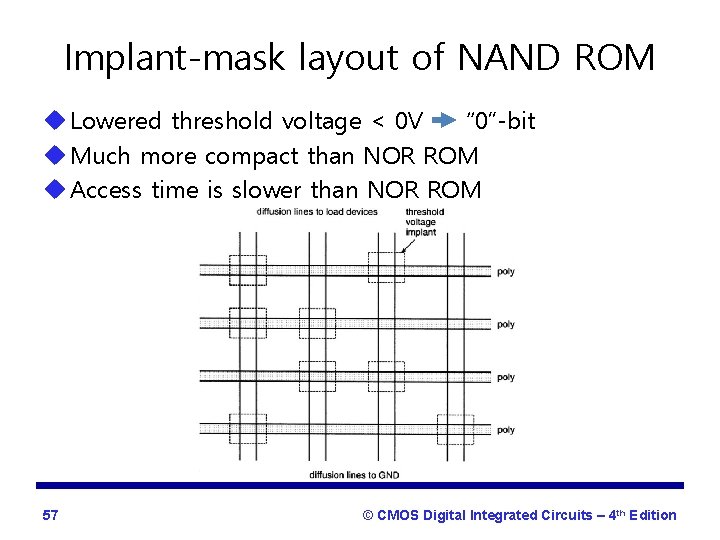
Implant-mask layout of NAND ROM u Lowered threshold voltage < 0 V “ 0”-bit u Much more compact than NOR ROM u Access time is slower than NOR ROM 57 © CMOS Digital Integrated Circuits – 4 th Edition

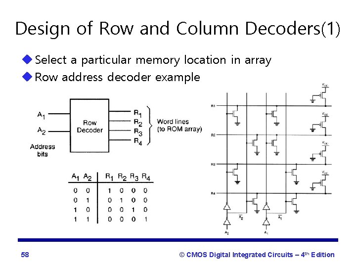
Design of Row and Column Decoders(1) u Select a particular memory location in array u Row address decoder example 58 © CMOS Digital Integrated Circuits – 4 th Edition

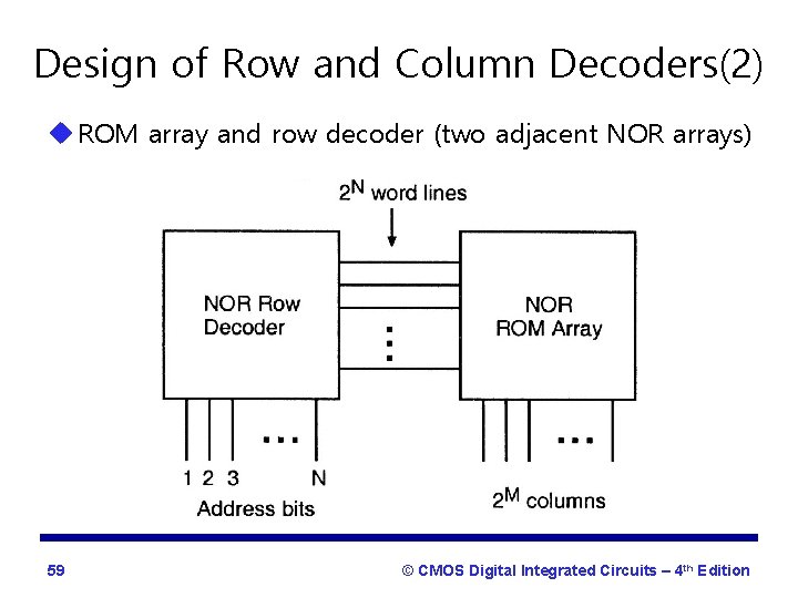
Design of Row and Column Decoders(2) u ROM array and row decoder (two adjacent NOR arrays) 59 © CMOS Digital Integrated Circuits – 4 th Edition

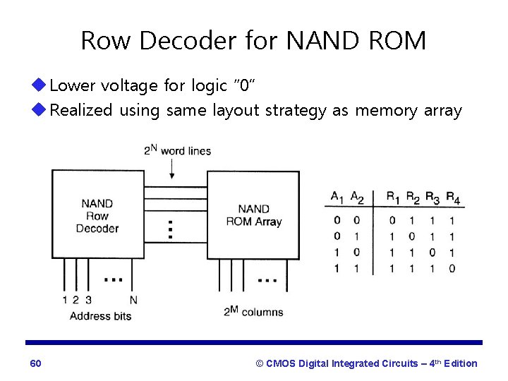
Row Decoder for NAND ROM u Lower voltage for logic “ 0” u Realized using same layout strategy as memory array 60 © CMOS Digital Integrated Circuits – 4 th Edition

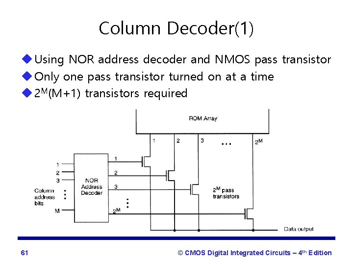
Column Decoder(1) u Using NOR address decoder and NMOS pass transistor u Only one pass transistor turned on at a time u 2 M(M+1) transistors required 61 © CMOS Digital Integrated Circuits – 4 th Edition

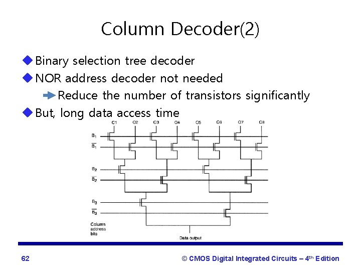
Column Decoder(2) u Binary selection tree decoder u NOR address decoder not needed Reduce the number of transistors significantly u But, long data access time 62 © CMOS Digital Integrated Circuits – 4 th Edition

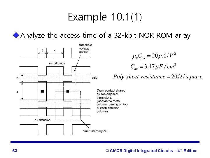
Example 10. 1(1) u Analyze the access time of a 32 -kbit NOR ROM array 63 © CMOS Digital Integrated Circuits – 4 th Edition

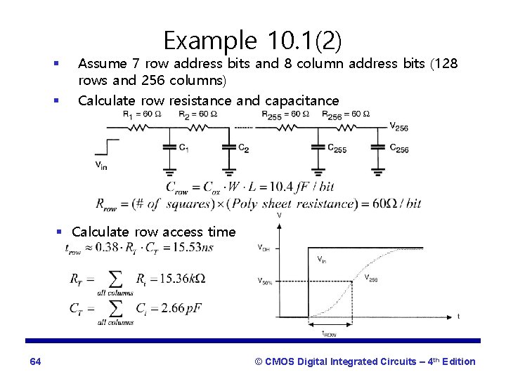
Example 10. 1(2) § § Assume 7 row address bits and 8 column address bits (128 rows and 256 columns) Calculate row resistance and capacitance § Calculate row access time 64 © CMOS Digital Integrated Circuits – 4 th Edition

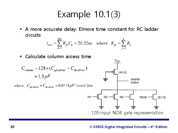
Example 10. 1(3) § A more accurate delay: Elmore time constant for RC ladder circuits § Calculate column access time 128 -input NOR gate representation 65 © CMOS Digital Integrated Circuits – 4 th Edition

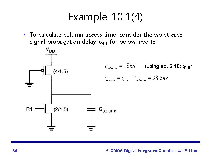
Example 10. 1(4) § To calculate column access time, consider the worst-case signal propagation delay τPHL for below inverter (using eq. 6. 18: t. PHL) 66 © CMOS Digital Integrated Circuits – 4 th Edition

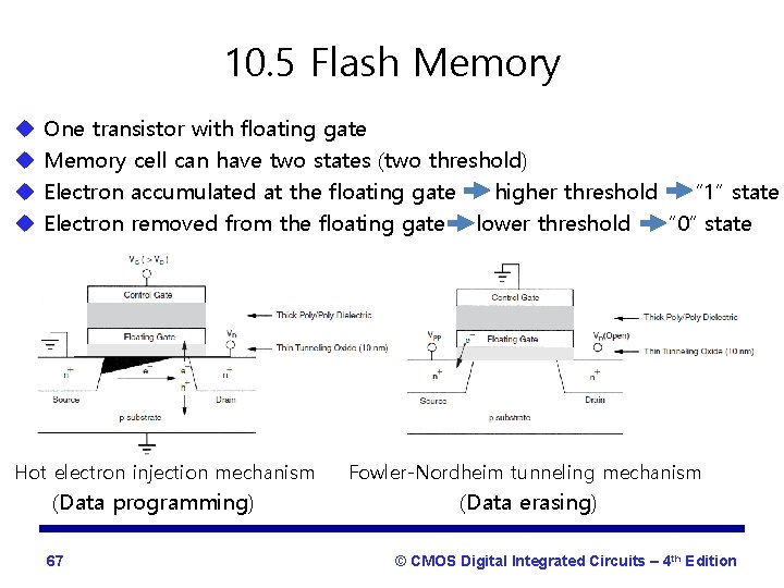
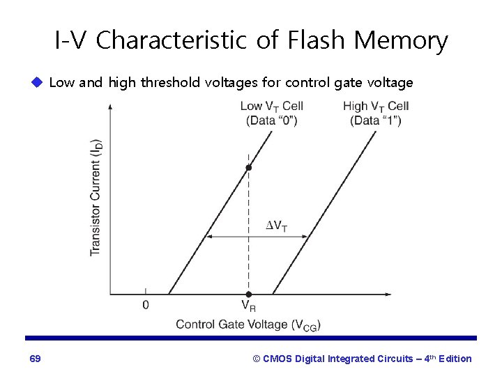
10. 5 Flash Memory u u One transistor with floating gate Memory cell can have two states (two threshold) Electron accumulated at the floating gate higher threshold “ 1” state Electron removed from the floating gate lower threshold “ 0” state Hot electron injection mechanism (Data programming) 67 Fowler-Nordheim tunneling mechanism (Data erasing) © CMOS Digital Integrated Circuits – 4 th Edition

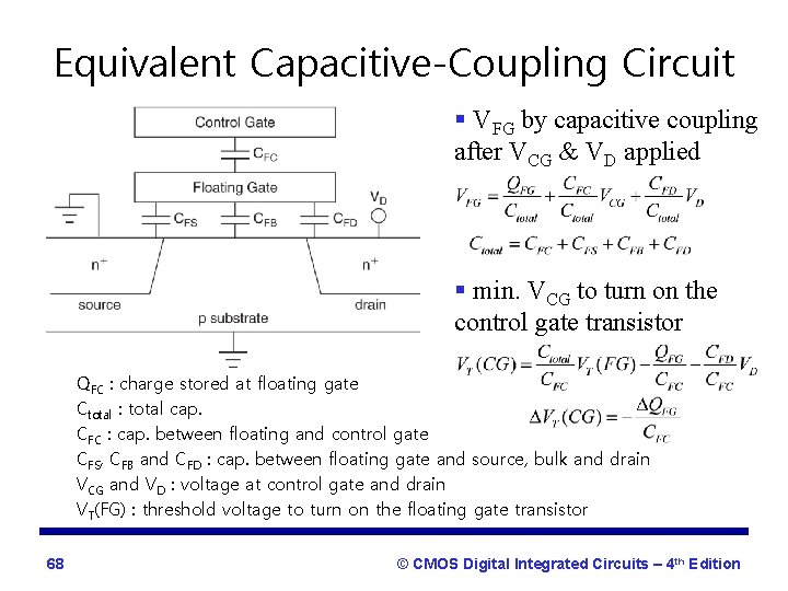
Equivalent Capacitive-Coupling Circuit § VFG by capacitive coupling after VCG & VD applied § min. VCG to turn on the control gate transistor QFC : charge stored at floating gate Ctotal : total cap. CFC : cap. between floating and control gate CFS, CFB and CFD : cap. between floating gate and source, bulk and drain VCG and VD : voltage at control gate and drain VT(FG) : threshold voltage to turn on the floating gate transistor 68 © CMOS Digital Integrated Circuits – 4 th Edition

I-V Characteristic of Flash Memory u Low and high threshold voltages for control gate voltage 69 © CMOS Digital Integrated Circuits – 4 th Edition

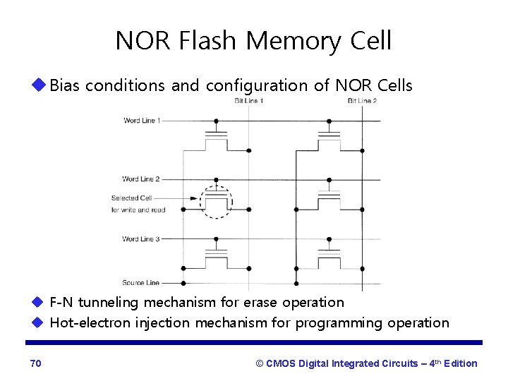
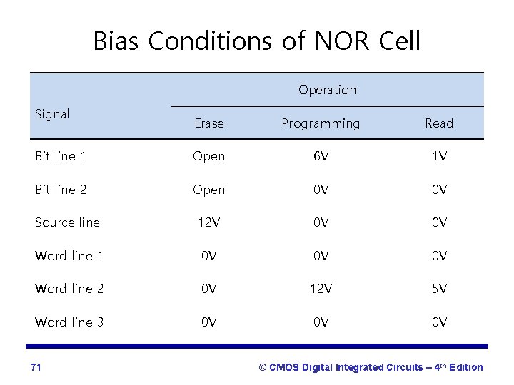
NOR Flash Memory Cell u Bias conditions and configuration of NOR Cells u F-N tunneling mechanism for erase operation u Hot-electron injection mechanism for programming operation 70 © CMOS Digital Integrated Circuits – 4 th Edition

Bias Conditions of NOR Cell Operation Signal Erase Programming Read Bit line 1 Open 6 V 1 V Bit line 2 Open 0 V 0 V Source line 12 V 0 V 0 V Word line 1 0 V 0 V 0 V Word line 2 0 V 12 V 5 V Word line 3 0 V 0 V 0 V 71 © CMOS Digital Integrated Circuits – 4 th Edition

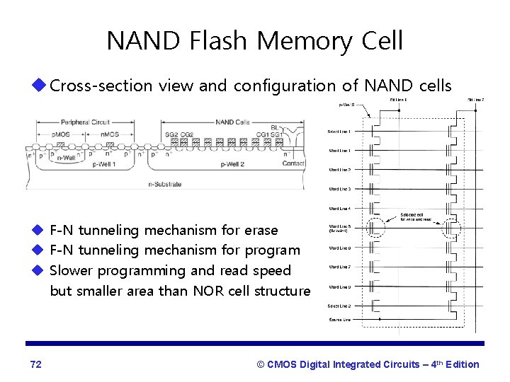
NAND Flash Memory Cell u Cross-section view and configuration of NAND cells u F-N tunneling mechanism for erase u F-N tunneling mechanism for program u Slower programming and read speed but smaller area than NOR cell structure 72 © CMOS Digital Integrated Circuits – 4 th Edition

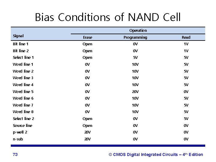
Bias Conditions of NAND Cell Operation Signal Erase Programming Read Bit line 1 Open 0 V 1 V Bit line 2 Open 0 V 1 V Select line 1 Open 5 V 5 V Word line 1 0 V 10 V 5 V Word line 2 0 V 10 V 5 V Word line 3 0 V 10 V 5 V Word line 4 0 V 10 V 5 V Word line 5 0 V 20 V 0 V Word line 6 0 V 10 V 5 V Word line 7 0 V 10 V 5 V Word line 8 0 V 10 V 5 V Select line 2 Open 0 V 5 V Source line Open 0 V 0 V p-well 2 20 V 0 V 0 V n-sub 20 V 0 V 0 V 73 © CMOS Digital Integrated Circuits – 4 th Edition

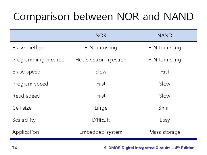
Comparison between NOR and NAND NOR NAND F-N tunneling Hot electron injection F-N tunneling Erase speed Slow Fast Program speed Fast Slow Read speed Fast Slow Large Small Difficult Easy Embedded system Mass storage Erase method Programming method Cell size Scalability Application 74 © CMOS Digital Integrated Circuits – 4 th Edition

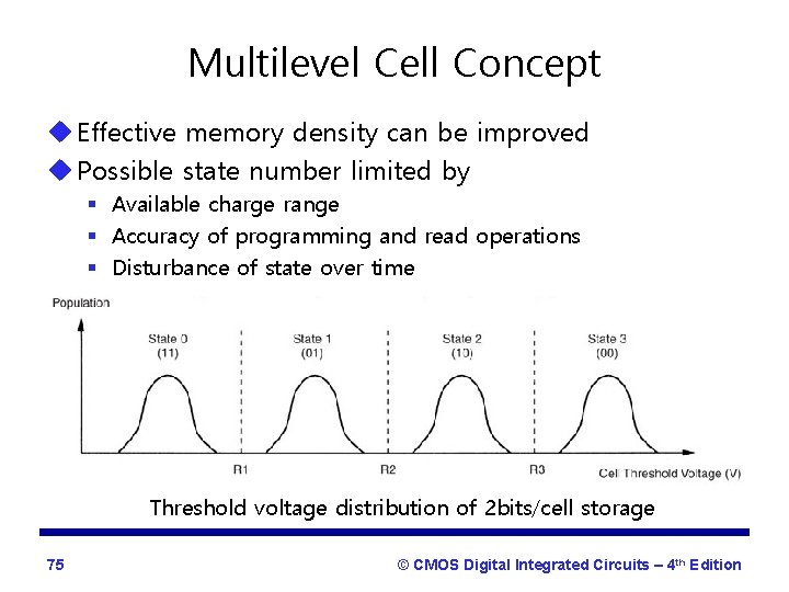
Multilevel Cell Concept u Effective memory density can be improved u Possible state number limited by § Available charge range § Accuracy of programming and read operations § Disturbance of state over time Threshold voltage distribution of 2 bits/cell storage 75 © CMOS Digital Integrated Circuits – 4 th Edition

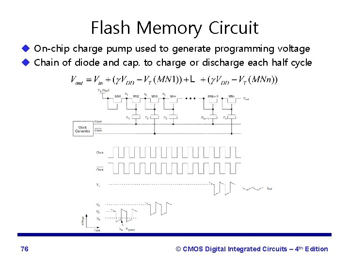
Flash Memory Circuit u On-chip charge pump used to generate programming voltage u Chain of diode and cap. to charge or discharge each half cycle 76 © CMOS Digital Integrated Circuits – 4 th Edition

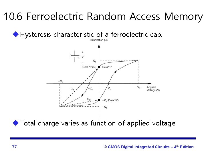
10. 6 Ferroelectric Random Access Memory u Hysteresis characteristic of a ferroelectric cap. u Total charge varies as function of applied voltage 77 © CMOS Digital Integrated Circuits – 4 th Edition

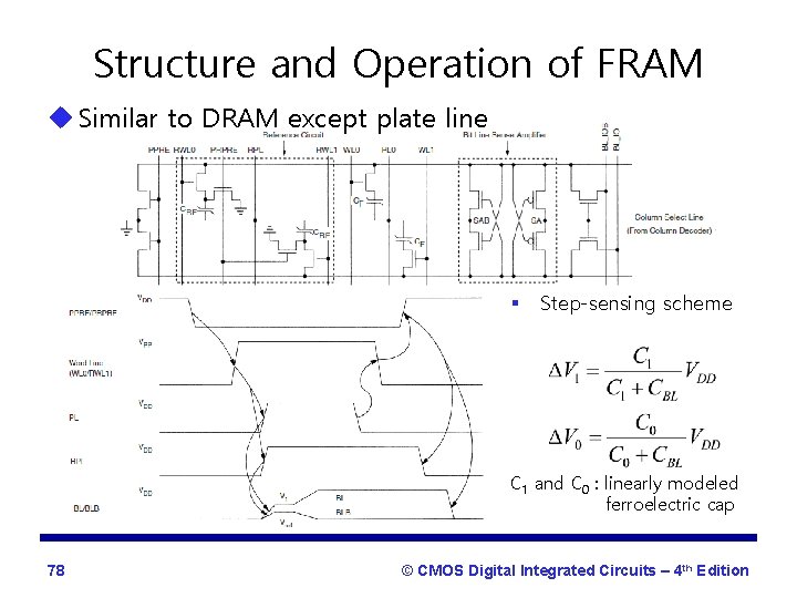
Structure and Operation of FRAM u Similar to DRAM except plate line § Step-sensing scheme C 1 and C 0 : linearly modeled ferroelectric cap 78 © CMOS Digital Integrated Circuits – 4 th Edition

Problems of FRAM u Step-sensing scheme cause reliability issues § Pulse sensing scheme also used with read speed penalty u Fatigue § Capacitance charge gradually degraded with repeated use u Imprint § Ferroelectric cap tends to stay at one state preferably when state maintained for a long time 79 © CMOS Digital Integrated Circuits – 4 th Edition