CMOS LogicGate Circuits 1 Static CMOS Circuits At


- Slides: 33

CMOS Logic-Gate Circuits 1

Static CMOS Circuits At every point in time (when input and output are stable) each gate output is connected to either VDD or Vss via a low-resistive path. The outputs of the gates assume at all times the value of the Boolean function, dependent of input signals (ignoring, once again, the transient effects during switching periods). They differ from the dynamic class circuits, which relies on temporary storage of signal values on the capacitance of high impedance circuit nodes. Microelectronic Circuits - Fifth Edition Sedra/Smith Copyright 2004 by Oxford University Press, Inc. 2

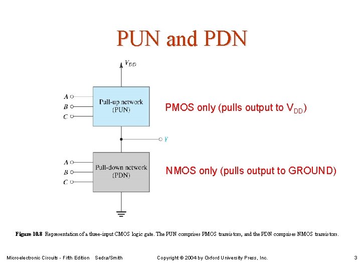
PUN and PDN PMOS only (pulls output to VDD) NMOS only (pulls output to GROUND) Figure 10. 8 Representation of a three-input CMOS logic gate. The PUN comprises PMOS transistors, and the PDN comprises NMOS transistors. Microelectronic Circuits - Fifth Edition Sedra/Smith Copyright 2004 by Oxford University Press, Inc. 3

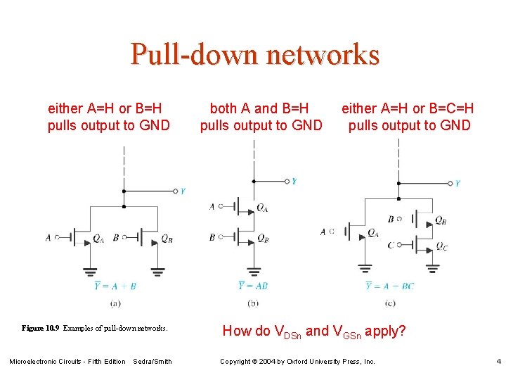
Pull-down networks either A=H or B=H pulls output to GND Figure 10. 9 Examples of pull-down networks. Microelectronic Circuits - Fifth Edition Sedra/Smith both A and B=H pulls output to GND either A=H or B=C=H pulls output to GND How do VDSn and VGSn apply? Copyright 2004 by Oxford University Press, Inc. 4

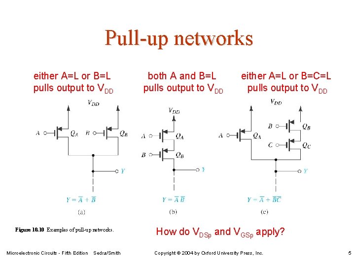
Pull-up networks either A=L or B=L pulls output to VDD Figure 10. 10 Examples of pull-up networks. Microelectronic Circuits - Fifth Edition Sedra/Smith both A and B=L pulls output to VDD either A=L or B=C=L pulls output to VDD How do VDSp and VGSp apply? Copyright 2004 by Oxford University Press, Inc. 5

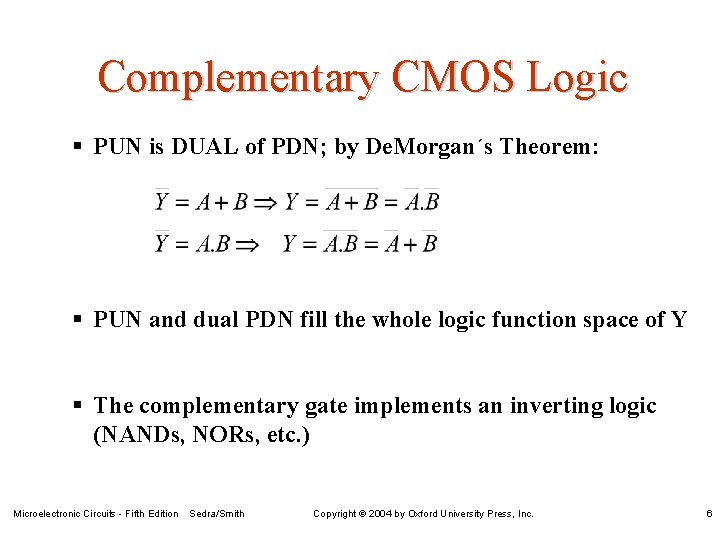
Complementary CMOS Logic § PUN is DUAL of PDN; by De. Morgan´s Theorem: § PUN and dual PDN fill the whole logic function space of Y § The complementary gate implements an inverting logic (NANDs, NORs, etc. ) Microelectronic Circuits - Fifth Edition Sedra/Smith Copyright 2004 by Oxford University Press, Inc. 6

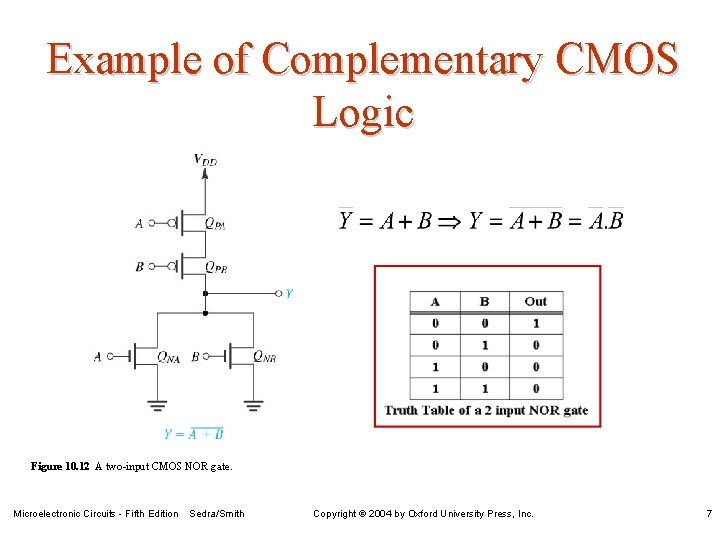
Example of Complementary CMOS Logic Figure 10. 12 A two-input CMOS NOR gate. Microelectronic Circuits - Fifth Edition Sedra/Smith Copyright 2004 by Oxford University Press, Inc. 7

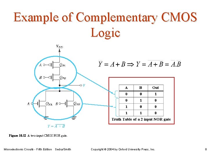
Example of Complementary CMOS Logic Figure 10. 12 A two-input CMOS NOR gate. Microelectronic Circuits - Fifth Edition Sedra/Smith Copyright 2004 by Oxford University Press, Inc. 8

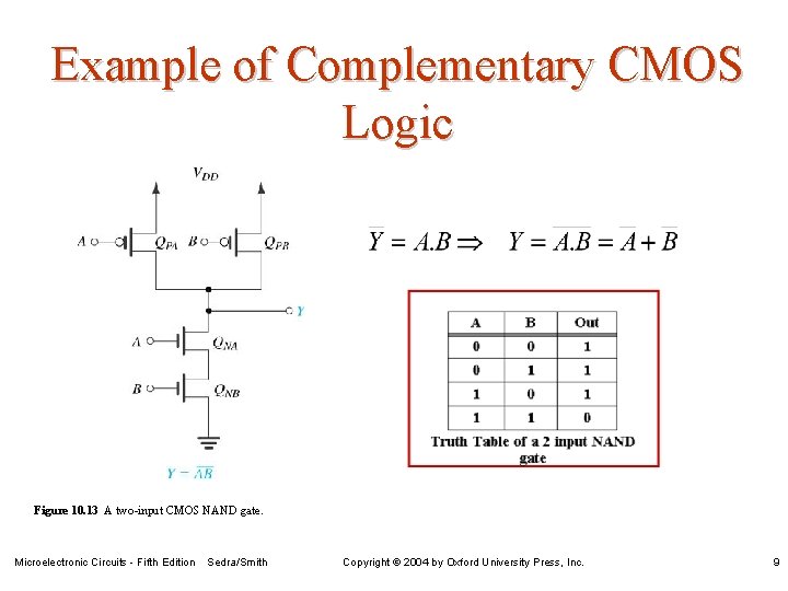
Example of Complementary CMOS Logic Figure 10. 13 A two-input CMOS NAND gate. Microelectronic Circuits - Fifth Edition Sedra/Smith Copyright 2004 by Oxford University Press, Inc. 9

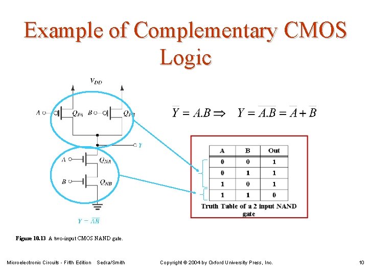
Example of Complementary CMOS Logic Figure 10. 13 A two-input CMOS NAND gate. Microelectronic Circuits - Fifth Edition Sedra/Smith Copyright 2004 by Oxford University Press, Inc. 10

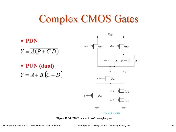
Complex CMOS Gates § PDN § PUN (dual) Figure 10. 14 CMOS realization of a complex gate. Microelectronic Circuits - Fifth Edition Sedra/Smith Copyright 2004 by Oxford University Press, Inc. 11

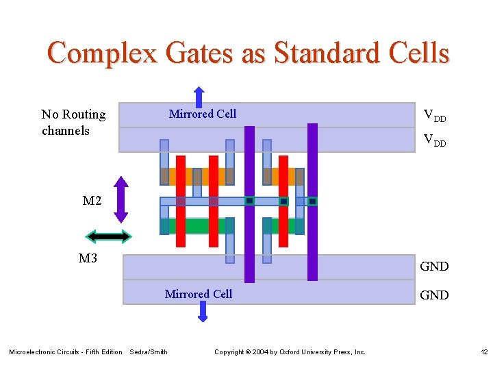
Complex Gates as Standard Cells No Routing channels Mirrored Cell VDD M 2 M 3 GND Mirrored Cell Microelectronic Circuits - Fifth Edition Sedra/Smith Copyright 2004 by Oxford University Press, Inc. GND 12

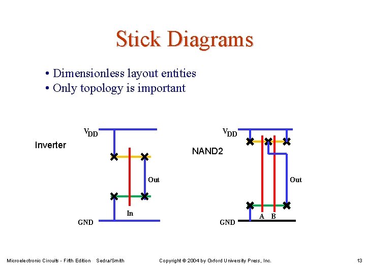
Stick Diagrams • Dimensionless layout entities • Only topology is important VDD Inverter NAND 2 Out In GND Microelectronic Circuits - Fifth Edition GND Sedra/Smith A B Copyright 2004 by Oxford University Press, Inc. 13

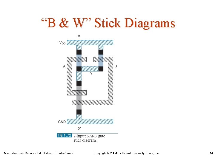
“B & W” Stick Diagrams Microelectronic Circuits - Fifth Edition Sedra/Smith Copyright 2004 by Oxford University Press, Inc. 14

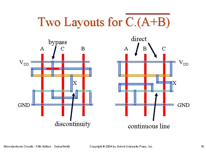
Two Layouts for C. (A+B) A direct bypass C B A B C VDD X X GND discontinuity Microelectronic Circuits - Fifth Edition Sedra/Smith continuous line Copyright 2004 by Oxford University Press, Inc. 15

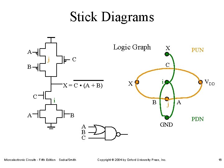
Stick Diagrams Logic Graph A j X C C B X = C • (A + B) C i A i X B VDD j B A B C Microelectronic Circuits - Fifth Edition Sedra/Smith PUN GND Copyright 2004 by Oxford University Press, Inc. A PDN 16

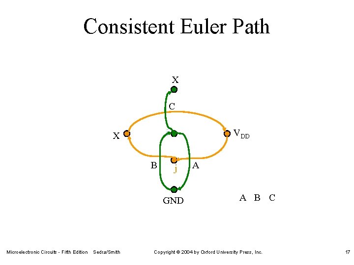
Consistent Euler Path X C i X B VDD j GND Microelectronic Circuits - Fifth Edition Sedra/Smith A A B C Copyright 2004 by Oxford University Press, Inc. 17

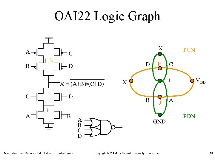
OAI 22 Logic Graph A B j k X C D D X = (A+B) • (C+D) C A D i Microelectronic Circuits - Fifth Edition B Sedra/Smith k C i X B A B C D PUN j GND Copyright 2004 by Oxford University Press, Inc. VDD A PDN 18

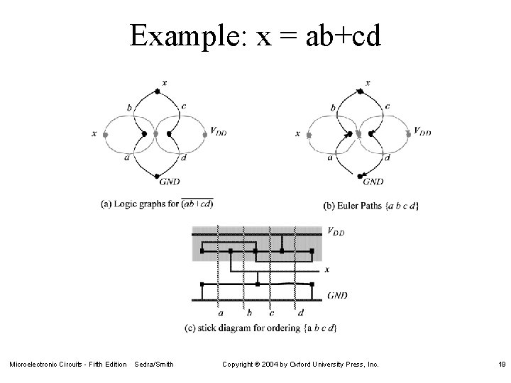
Example: x = ab+cd Microelectronic Circuits - Fifth Edition Sedra/Smith Copyright 2004 by Oxford University Press, Inc. 19

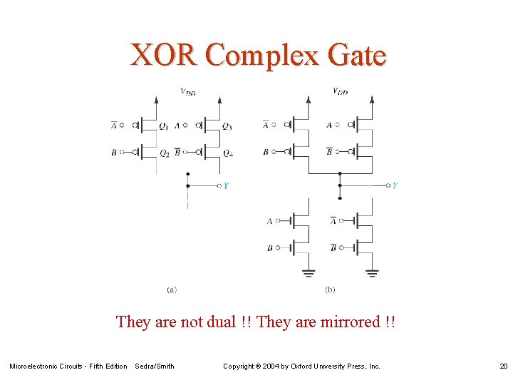
XOR Complex Gate They are not dual !! They are mirrored !! Microelectronic Circuits - Fifth Edition Sedra/Smith Copyright 2004 by Oxford University Press, Inc. 20

Resistance-Switch Delay Model-1 Reqn X X closes on X=1 What are the values for VGSn and VDSn? What are the dependencies for Reqn with respect to Wn, Ln , CL, VDD and mn? Microelectronic Circuits - Fifth Edition Sedra/Smith Copyright 2004 by Oxford University Press, Inc. 21

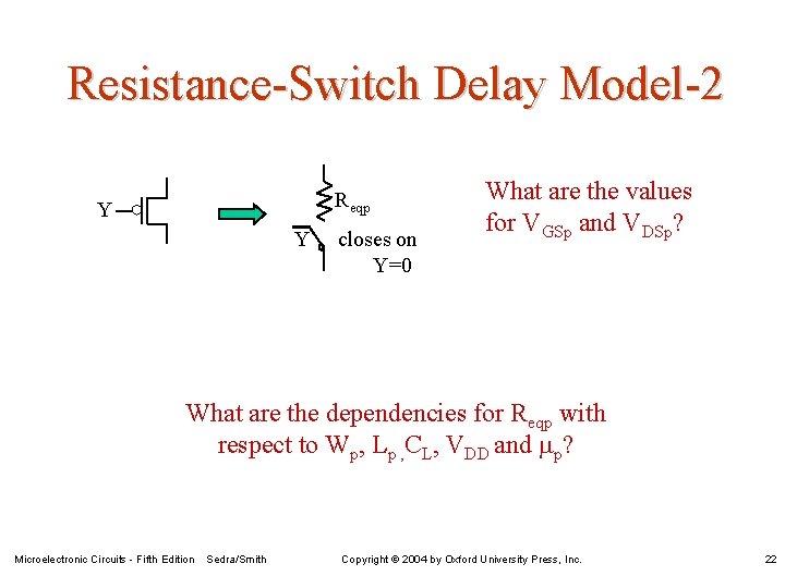
Resistance-Switch Delay Model-2 Reqp Y Y closes on Y=0 What are the values for VGSp and VDSp? What are the dependencies for Reqp with respect to Wp, Lp , CL, VDD and mp? Microelectronic Circuits - Fifth Edition Sedra/Smith Copyright 2004 by Oxford University Press, Inc. 22

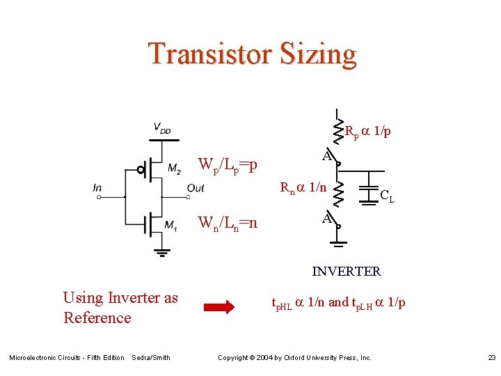
Transistor Sizing Rp a 1/p Wp/Lp=p A Rn a 1/n Wn/Ln=n CL A INVERTER Using Inverter as Reference Microelectronic Circuits - Fifth Edition Sedra/Smith tp. HL a 1/n and tp. LH a 1/p Copyright 2004 by Oxford University Press, Inc. 23

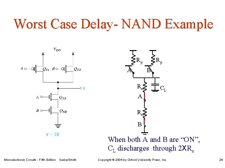
Worst Case Delay- NAND Example Rp A Rp B Rn CL A Rn B When both A and B are “ON”, CL discharges through 2 XRn Microelectronic Circuits - Fifth Edition Sedra/Smith Copyright 2004 by Oxford University Press, Inc. 24

Worst Case Delay- NAND Example Rp A Rp B Rn Wn/Ln=n A Wn/Ln=n Rn B CL Rtotal=2 XRn a 2/n, therefore t. PHL=2 Xtp. HL(inverter) When both A and B are “ON”, CL discharges through 2 XRn Microelectronic Circuits - Fifth Edition Sedra/Smith Copyright 2004 by Oxford University Press, Inc. 25

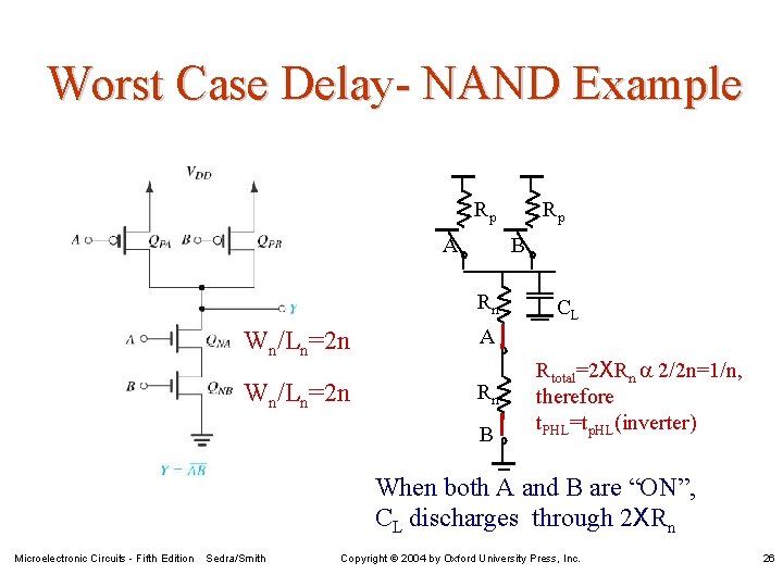
Worst Case Delay- NAND Example Rp A Rp B Rn Wn/Ln=2 n A Wn/Ln=2 n Rn B CL Rtotal=2 XRn a 2/2 n=1/n, therefore t. PHL=tp. HL(inverter) When both A and B are “ON”, CL discharges through 2 XRn Microelectronic Circuits - Fifth Edition Sedra/Smith Copyright 2004 by Oxford University Press, Inc. 26

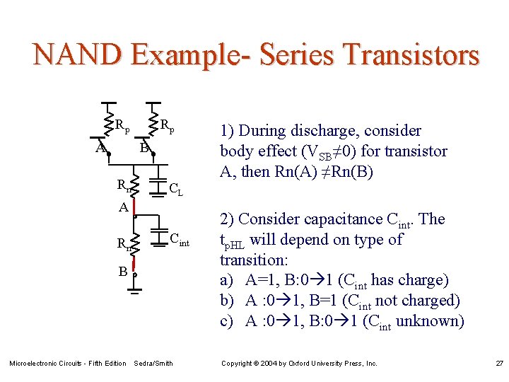
NAND Example- Series Transistors Rp A Rp B Rn CL A Rn Cint B Microelectronic Circuits - Fifth Edition Sedra/Smith 1) During discharge, consider body effect (VSB≠ 0) for transistor A, then Rn(A) ≠Rn(B) 2) Consider capacitance Cint. The tp. HL will depend on type of transition: a) A=1, B: 0 1 (Cint has charge) b) A : 0 1, B=1 (Cint not charged) c) A : 0 1, B: 0 1 (Cint unknown) Copyright 2004 by Oxford University Press, Inc. 27

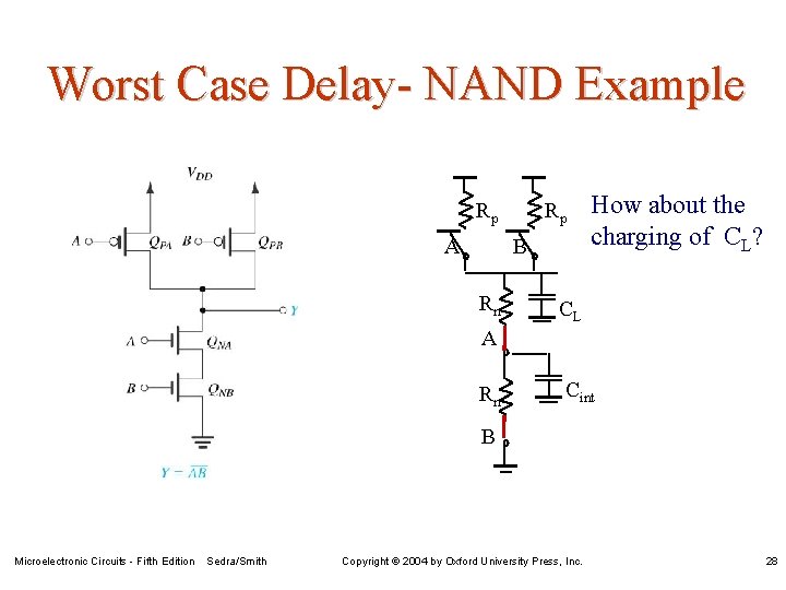
Worst Case Delay- NAND Example Rp A Rp B Rn How about the charging of CL? CL A Rn Cint B Microelectronic Circuits - Fifth Edition Sedra/Smith Copyright 2004 by Oxford University Press, Inc. 28

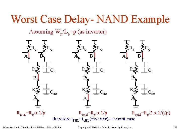
Worst Case Delay- NAND Example Assuming Wp/Lp=p (as inverter) Rp A Rp Rp A B Rn CL B Rn A Rtotal=Rp a 1/p Microelectronic Circuits - Fifth Edition A B Rn CL Rn A Rp B Rn CL B B Cint Rp Rp Cint Rn A Cint Rtotal=Rp a 1/p Rtotal=Rp/2 a 1/(2 p) therefore t. PHL=tp. HL(inverter) at worst case Sedra/Smith Copyright 2004 by Oxford University Press, Inc. 29

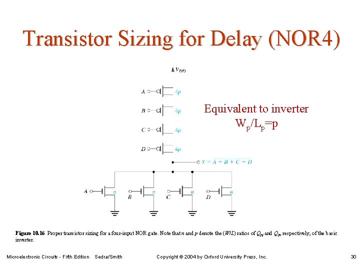
Transistor Sizing for Delay (NOR 4) Equivalent to inverter Wp/Lp=p Figure 10. 16 Proper transistor sizing for a four-input NOR gate. Note that n and p denote the (W/L) ratios of QN and QP, respectively, of the basic inverter. Microelectronic Circuits - Fifth Edition Sedra/Smith Copyright 2004 by Oxford University Press, Inc. 30

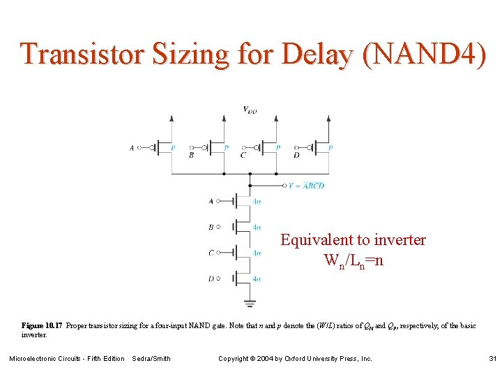
Transistor Sizing for Delay (NAND 4) Equivalent to inverter Wn/Ln=n Figure 10. 17 Proper transistor sizing for a four-input NAND gate. Note that n and p denote the (W/L) ratios of QN and QP, respectively, of the basic inverter. Microelectronic Circuits - Fifth Edition Sedra/Smith Copyright 2004 by Oxford University Press, Inc. 31

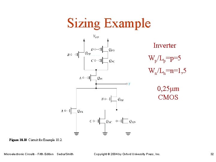
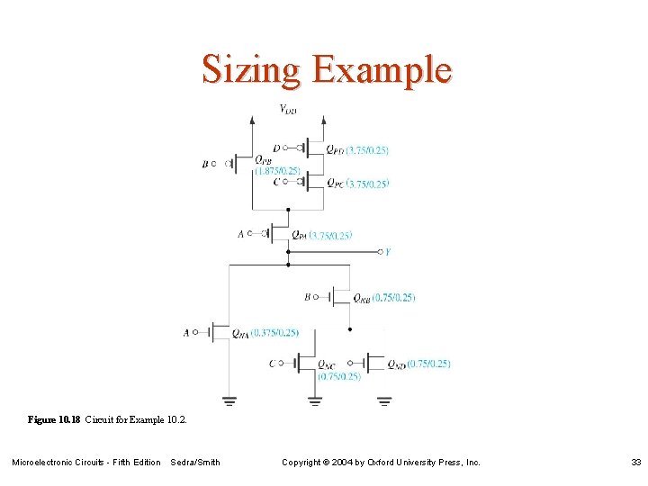
Sizing Example Inverter Wp/Lp=p=5 Wn/Ln=n=1, 5 0, 25 mm CMOS Figure 10. 18 Circuit for Example 10. 2. Microelectronic Circuits - Fifth Edition Sedra/Smith Copyright 2004 by Oxford University Press, Inc. 32

Sizing Example Figure 10. 18 Circuit for Example 10. 2. Microelectronic Circuits - Fifth Edition Sedra/Smith Copyright 2004 by Oxford University Press, Inc. 33