Circuit Characterization and Performance Estimation CMOS circuit performance
- Slides: 23

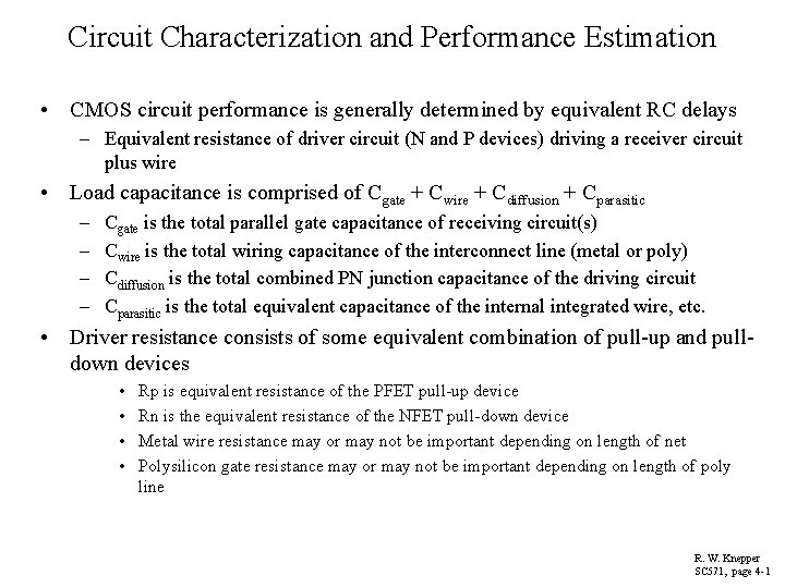
Circuit Characterization and Performance Estimation • CMOS circuit performance is generally determined by equivalent RC delays – Equivalent resistance of driver circuit (N and P devices) driving a receiver circuit plus wire • Load capacitance is comprised of Cgate + Cwire + Cdiffusion + Cparasitic – – Cgate is the total parallel gate capacitance of receiving circuit(s) Cwire is the total wiring capacitance of the interconnect line (metal or poly) Cdiffusion is the total combined PN junction capacitance of the driving circuit Cparasitic is the total equivalent capacitance of the internal integrated wire, etc. • Driver resistance consists of some equivalent combination of pull-up and pulldown devices • • Rp is equivalent resistance of the PFET pull-up device Rn is the equivalent resistance of the NFET pull-down device Metal wire resistance may or may not be important depending on length of net Polysilicon gate resistance may or may not be important depending on length of poly line R. W. Knepper SC 571, page 4 -1

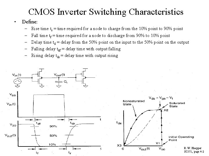
CMOS Inverter Switching Characteristics • Define: – – – Rise time tr = time required for a node to charge from the 10% point to 90% point Fall time tf = time required for a node to discharge from 90% to 10% point Delay time td = delay from the 50% point on the input to the 50% point on the output Falling delay tdf = delay time with output falling Rising delay tdr = delay time with output rising R. W. Knepper SC 571, page 4 -2

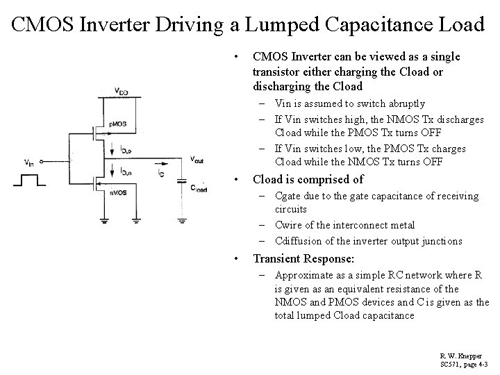
CMOS Inverter Driving a Lumped Capacitance Load • CMOS Inverter can be viewed as a single transistor either charging the Cload or discharging the Cload – Vin is assumed to switch abruptly – If Vin switches high, the NMOS Tx discharges Cload while the PMOS Tx turns OFF – If Vin switches low, the PMOS Tx charges Cload while the NMOS Tx turns OFF • Cload is comprised of – Cgate due to the gate capacitance of receiving circuits – Cwire of the interconnect metal – Cdiffusion of the inverter output junctions • Transient Response: – Approximate as a simple RC network where R is given as an equivalent resistance of the NMOS and PMOS devices and C is given as the total lumped Cload capacitance R. W. Knepper SC 571, page 4 -3

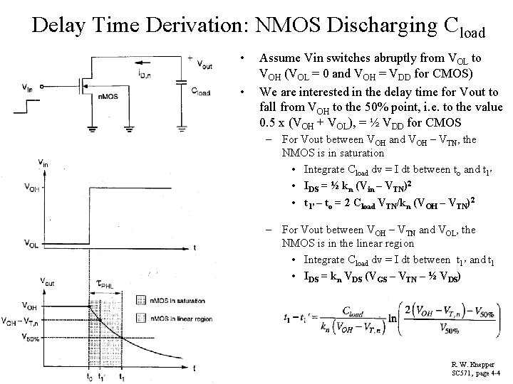
Delay Time Derivation: NMOS Discharging Cload • • Assume Vin switches abruptly from VOL to VOH (VOL = 0 and VOH = VDD for CMOS) We are interested in the delay time for Vout to fall from VOH to the 50% point, i. e. to the value 0. 5 x (VOH + VOL), = ½ VDD for CMOS – For Vout between VOH and VOH – VTN, the NMOS is in saturation • Integrate Cload dv = I dt between to and t 1’ • IDS = ½ kn (Vin – VTN)2 • t 1’ – to = 2 Cload VTN/kn (VOH – VTN)2 – For Vout between VOH – VTN and VOL, the NMOS is in the linear region • Integrate Cload dv = I dt between t 1’ and t 1 • IDS = kn VDS (VGS – VTN – ½ VDS) R. W. Knepper SC 571, page 4 -4

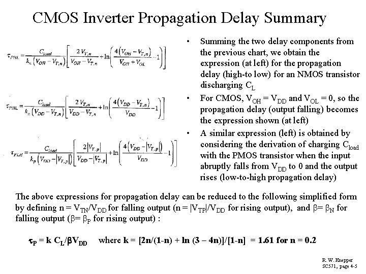
CMOS Inverter Propagation Delay Summary • • • Summing the two delay components from the previous chart, we obtain the expression (at left) for the propagation delay (high-to low) for an NMOS transistor discharging CL For CMOS, VOH = VDD and VOL = 0, so the propagation delay (output falling) becomes the expression shown (at left) A similar expression (left) is obtained by considering the derivation of charging Cload with the PMOS transistor when the input abruptly falls from VDD to 0 and the output rises (low-to-high propagation delay) The above expressions for propagation delay can be reduced to the following simplified form by defining n = VTN/VDD for falling output (n = |VTP|/VDD for rising output), and = N for falling output ( = P for rising output) : P = k CL/ VDD where k = [2 n/(1 -n) + ln (3 – 4 n)]/[1 -n] = 1. 61 for n = 0. 2 R. W. Knepper SC 571, page 4 -5

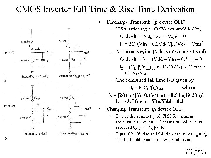
CMOS Inverter Fall Time & Rise Time Derivation • Discharge Transient: (p device OFF) – N Saturation region (0. 9 Vdd>vout>Vdd-Vtn) CLdv/dt + ½ n (Vdd – Vtn)2 = 0 t 1 = 2 CL(Vtn – 0. 1 Vdd)/ n(Vdd – Vtn)2 – N Linear Region (Vdd-Vtn>vout>0. 1 Vdd) CLdv/dt + n v (Vdd – Vtn – 0. 5 v) = 0 t 2 = (CL/ n. Vdd)[{ln (19 -20 n)}/{1 -n}] where n = Vtn/Vdd • – The combined fall time tf is given by tf = k CL/ n. Vdd where k = [2/(1 -n)][(n-0. 1)/(1 -n) + 0. 5 ln(19 -20 n)] k = ~3. 7 for n = Vtn/Vdd = 0. 2 Charging Transient: (n device OFF) • • Due to the symmetry of CMOS, a similar expression is obtained for rise time where n is replaced by p = |Vtp|/Vdd Equal CMOS rise and fall times requires n = p due to the difference in e & h mobilities. R. W. Knepper SC 571, page 4 -6

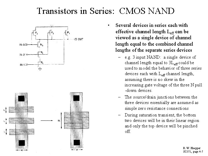
Transistors in Series: CMOS NAND • Several devices in series each with effective channel length Leff can be viewed as a single device of channel length equal to the combined channel lengths of the separate series devices – e. g. 3 input NAND: a single device of channel length equal to 3 Leff could be used to model the behavior of three series devices each with Leff channel length, assuming there is no skew in the increasing gate voltage of the three N pull -down devices. – The source/drain junctions between the three devices essentially are assumed as simple zero resistance connections – During saturation transient, the bottom two devices will be in their linear region and only the top device will be pinched off. R. W. Knepper SC 571, page 4 -7

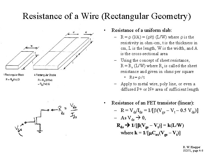
Resistance of a Wire (Rectangular Geometry) • Resistance of a uniform slab: – R = (l/A) = ( /t) (L/W) where is the resistivity in ohm-cm, t is the thickness in cm, L is the length, W is the width, and A is the cross-sectional area – Using the concept of sheet resistance, R = Rs (L/W) where Rs is called the sheet resistance and given in ohms per square • Rs = / t – Apply to metal wire, poly line, or even a diffused P+ or N+ area of sufficient length • Resistance of an FET transistor (linear): – R = Vds/Ids = 1/[ (Vgs – Vt – 0. 5 Vds)] – As Vds 0, Rds 1/[ (Vgs – Vt)] = k(L/W) where k = 1/[ Cox(Vgs – Vt)] R. W. Knepper SC 571, page 4 -8

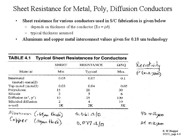
Sheet Resistance for Metal, Poly, Diffusion Conductors • Sheet resistance for various conductors used in S/C fabrication is given below – depends on thickness of the conductor (Rs = /t) – typical thickness assumed • Aluminum and copper metal interconnect values given for 0. 18 um technology R. W. Knepper SC 571, page 4 -9

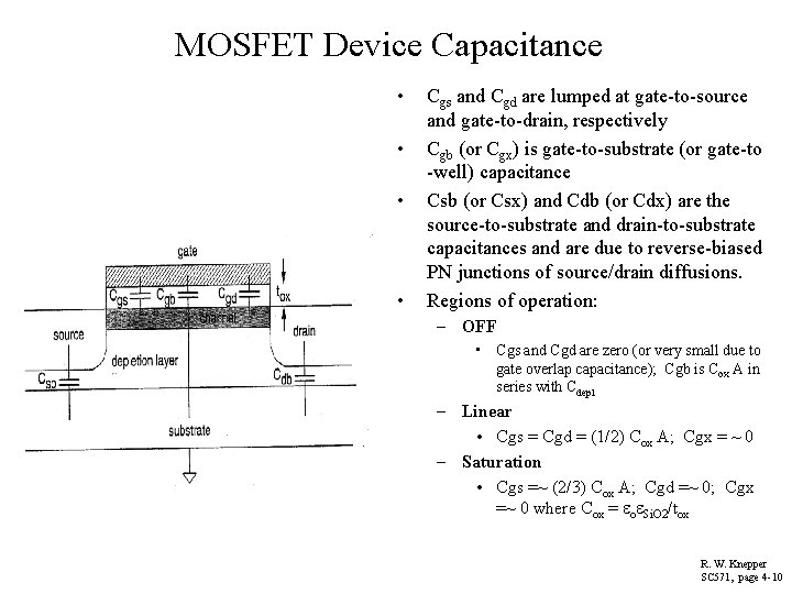
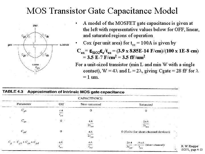
MOSFET Device Capacitance • • Cgs and Cgd are lumped at gate-to-source and gate-to-drain, respectively Cgb (or Cgx) is gate-to-substrate (or gate-to -well) capacitance Csb (or Csx) and Cdb (or Cdx) are the source-to-substrate and drain-to-substrate capacitances and are due to reverse-biased PN junctions of source/drain diffusions. Regions of operation: – OFF • Cgs and Cgd are zero (or very small due to gate overlap capacitance); Cgb is Cox A in series with Cdepl – Linear • Cgs = Cgd = (1/2) Cox A; Cgx = ~ 0 – Saturation • Cgs =~ (2/3) Cox A; Cgd =~ 0; Cgx =~ 0 where Cox = o Si. O 2/tox R. W. Knepper SC 571, page 4 -10

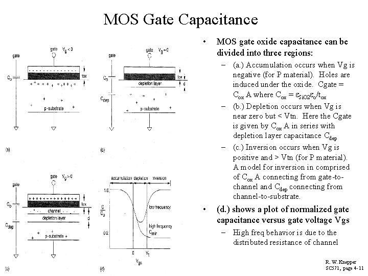
MOS Gate Capacitance • MOS gate oxide capacitance can be divided into three regions: – (a. ) Accumulation occurs when Vg is negative (for P material). Holes are induced under the oxide. Cgate = Cox A where Cox = Si. O 2 o/tox – (b. ) Depletion occurs when Vg is near zero but < Vtn. Here the Cgate is given by Cox A in series with depletion layer capacitance Cdep – (c. ) Inversion occurs when Vg is positive and > Vtn (for P material). A model for inversion in comprised of Cox A connecting from gate-tochannel and Cdep connecting from channel-to-substrate. • (d. ) shows a plot of normalized gate capacitance versus gate voltage Vgs – High freq behavior is due to the distributed resistance of channel R. W. Knepper SC 571, page 4 -11

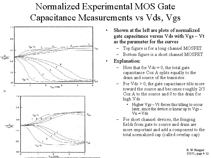
Normalized Experimental MOS Gate Capacitance Measurements vs Vds, Vgs • Shown at the left are plots of normalized gate capacitance versus Vds with Vgs – Vt as the parameter for the curves – Top figure is for a long channel MOSFET – Bottom figure is a short channel MOSFET • Explanation: – Note that for Vds = 0, the total gate capacitance Cox A splits equally to the drain and source of the transistor. – For Vds > 0, the gate capacitance tilts more toward the source and becomes roughly 2/3 Cox A to the source and 0 to the drain for high Vds • Higher Vgs – Vt forces this tilting to occur later, since the device is linear up to Vgs – Vn = Vds – For short channel devices, the fringing fields from gate to source and drain are more important and add a component to the total normalized cap (called overlap cap) R. W. Knepper SC 571, page 4 -12

MOS Transistor Gate Capacitance Model • • A model of the MOSFET gate capacitance is given at the left with representative values below for OFF, linear, and saturated regions of operation Cox (per unit area) for tox = 100 A is given by Cox= Si. O 2 o/tox = (3. 9 x 8. 85 E-14 F/cm)/(100 x 1 E-8 cm) = 3. 5 E-7 F/cm 2 = 3. 5 f. F/um 2 For a unit-sized transistor (min L and min W with a single contact), W = 4 and L = 2 , giving Cgate = 28 f. F for = 1 um. R. W. Knepper SC 571, page 4 -13

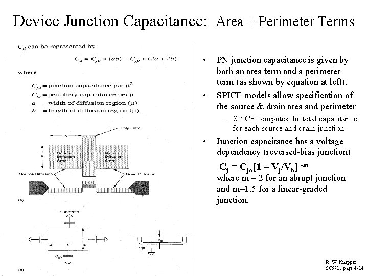
Device Junction Capacitance: Area + Perimeter Terms • • PN junction capacitance is given by both an area term and a perimeter term (as shown by equation at left). SPICE models allow specification of the source & drain area and perimeter – SPICE computes the total capacitance for each source and drain junction • Junction capacitance has a voltage dependency (reversed-bias junction) Cj = Cjo[1 – Vj/Vb] -m where m = 2 for an abrupt junction and m=1. 5 for a linear-graded junction. R. W. Knepper SC 571, page 4 -14

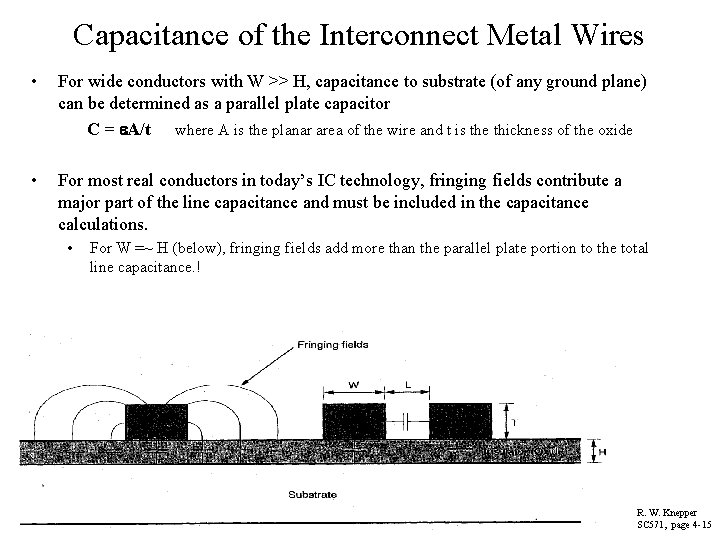
Capacitance of the Interconnect Metal Wires • For wide conductors with W >> H, capacitance to substrate (of any ground plane) can be determined as a parallel plate capacitor C = A/t where A is the planar area of the wire and t is the thickness of the oxide • For most real conductors in today’s IC technology, fringing fields contribute a major part of the line capacitance and must be included in the capacitance calculations. • For W =~ H (below), fringing fields add more than the parallel plate portion to the total line capacitance. ! R. W. Knepper SC 571, page 4 -15

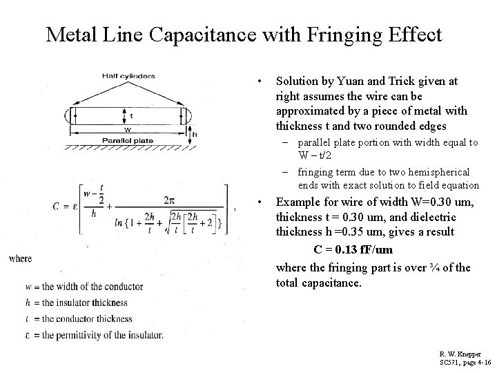
Metal Line Capacitance with Fringing Effect • Solution by Yuan and Trick given at right assumes the wire can be approximated by a piece of metal with thickness t and two rounded edges – parallel plate portion with width equal to W – t/2 – fringing term due to two hemispherical ends with exact solution to field equation • Example for wire of width W=0. 30 um, thickness t = 0. 30 um, and dielectric thickness h =0. 35 um, gives a result C = 0. 13 f. F/um where the fringing part is over ¾ of the total capacitance. R. W. Knepper SC 571, page 4 -16

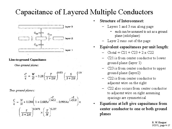
Capacitance of Layered Multiple Conductors • Structure of Interconnect: – Layers 1 and 3 run along page • each can be assumed to act as a ground plane (solid plane) – Layer 2 runs out of the page • Equivalent capacitances per unit length: – Ctotal = C 21 + C 23 + 2 x C 22 – C 21 is from center conductor to lower ground plane (layer 1) – C 23 is from center conductor to upper ground plane (layer 2) – C 22 is from center conductor to adjacent wire on the right – C 22 also occurs from center conductor to adjacent wire on right assuming spacings are symmetrical • Equations at left give capacitance from center conductor to one or both ground planes R. W. Knepper SC 571, page 4 -17

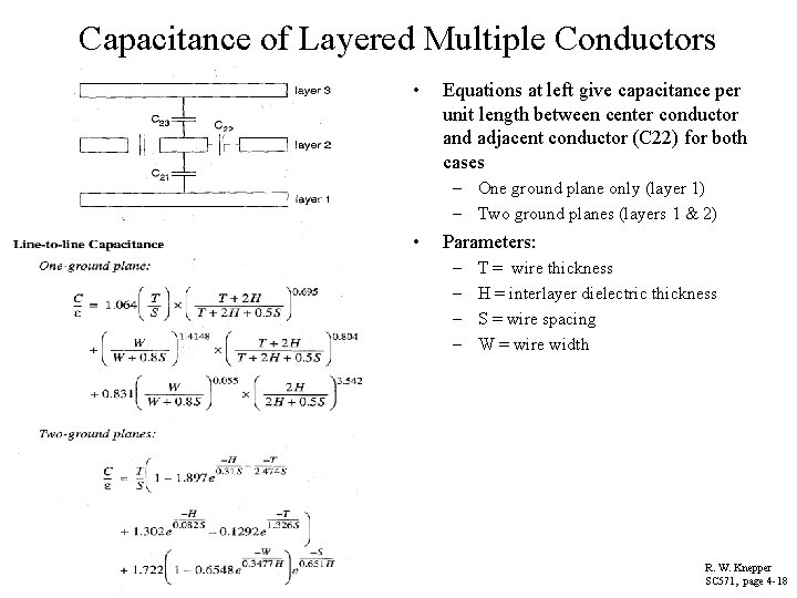
Capacitance of Layered Multiple Conductors • Equations at left give capacitance per unit length between center conductor and adjacent conductor (C 22) for both cases – One ground plane only (layer 1) – Two ground planes (layers 1 & 2) • Parameters: – – T = wire thickness H = interlayer dielectric thickness S = wire spacing W = wire width R. W. Knepper SC 571, page 4 -18

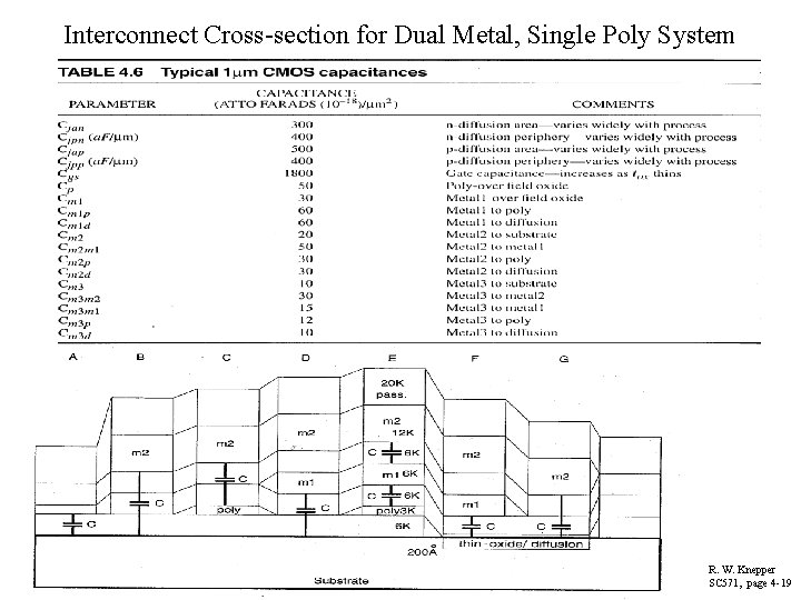
Interconnect Cross-section for Dual Metal, Single Poly System R. W. Knepper SC 571, page 4 -19

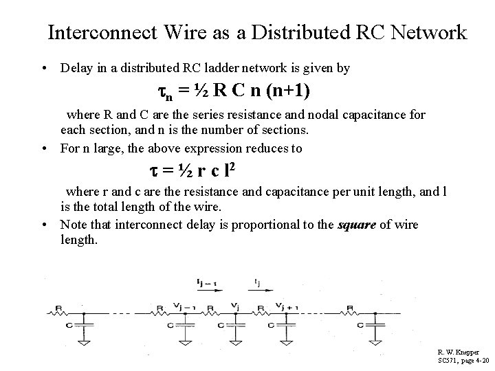
Interconnect Wire as a Distributed RC Network • Delay in a distributed RC ladder network is given by n = ½ R C n (n+1) where R and C are the series resistance and nodal capacitance for each section, and n is the number of sections. • For n large, the above expression reduces to = ½ r c l 2 where r and c are the resistance and capacitance per unit length, and l is the total length of the wire. • Note that interconnect delay is proportional to the square of wire length. R. W. Knepper SC 571, page 4 -20

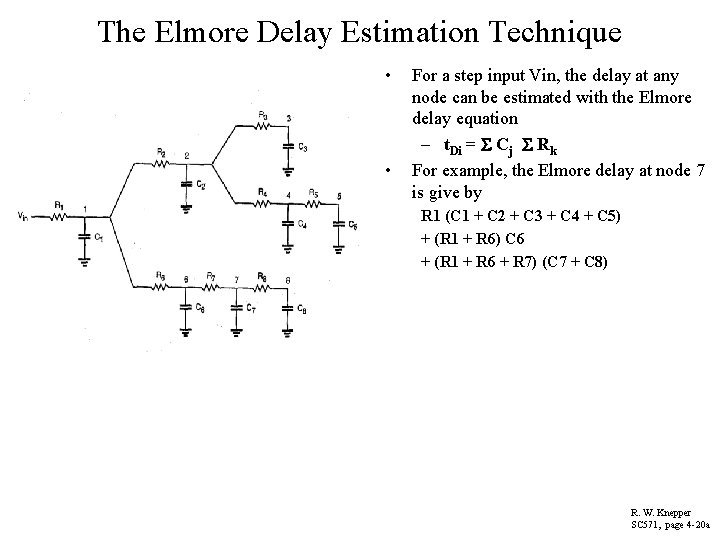
The Elmore Delay Estimation Technique • • For a step input Vin, the delay at any node can be estimated with the Elmore delay equation – t. Di = Cj Rk For example, the Elmore delay at node 7 is give by R 1 (C 1 + C 2 + C 3 + C 4 + C 5) + (R 1 + R 6) C 6 + (R 1 + R 6 + R 7) (C 7 + C 8) R. W. Knepper SC 571, page 4 -20 a

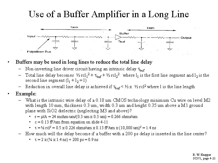
Use of a Buffer Amplifier in a Long Line • Buffers may be used in long lines to reduce the total line delay – Non-inverting line driver circuit having an intrinsic delay buf – Total line delay becomes ½ rcl 12 + buf + ½ rcl 22 where l 1 is the first line segment and l 2 is the second line segment (l 1 + l 2 = l) – Reduction in overall line delay is achieved if buf < ½ x ½ rcl 2 where l is the line length • Example: – What is the intrinsic wire delay of a 0. 18 um CMOS technology minimum Cu wire on level M 2 with length 10 mm, thickness 0. 3 um, width 0. 3 um and height 0. 35 um above a M 1 ground plane with Si. O 2 dielectric (neglecting M 3 and above)? • r = /A = 24 mohm-um/(0. 3 um x 0. 3 um) = 0. 266 ohms/um • c = 0. 13 f. F/um from equation on slide 4 -11 • = ½ rcl 2 = 0. 5 x 0. 226 ohms/um x 0. 13 f. F/um x (10, 000 um)2 = 1. 4 ns – How much will the delay become if a buffer with a 200 ps delay is inserted in the line center? • = 2 x (¼ x 1. 4 ns) + 200 ps = 0. 9 ns R. W. Knepper SC 571, page 4 -21

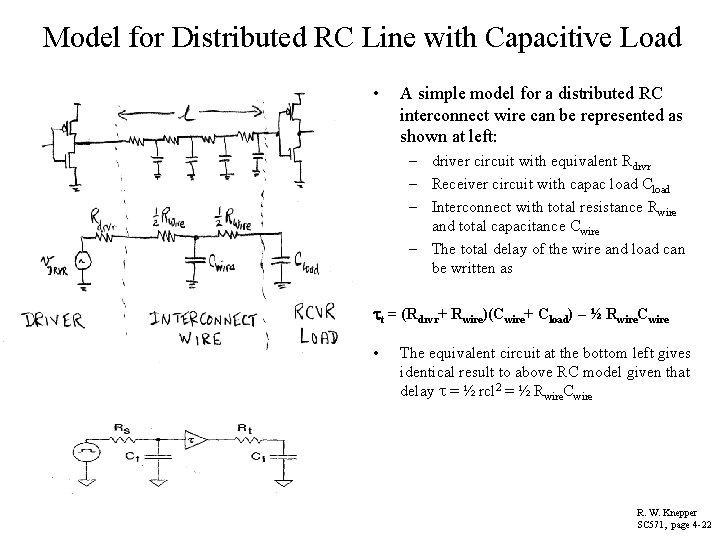
Model for Distributed RC Line with Capacitive Load • A simple model for a distributed RC interconnect wire can be represented as shown at left: – driver circuit with equivalent Rdrvr – Receiver circuit with capac load Cload – Interconnect with total resistance Rwire and total capacitance Cwire – The total delay of the wire and load can be written as t = (Rdrvr+ Rwire)(Cwire+ Cload) – ½ Rwire. Cwire • The equivalent circuit at the bottom left gives identical result to above RC model given that delay = ½ rcl 2 = ½ Rwire. Cwire R. W. Knepper SC 571, page 4 -22