Chapter 6 I CMOS Layout of Complexe Gate
- Slides: 17

Chapter 6 (I) CMOS Layout of Complexe Gate Designing Combinational Logic Circuits March 28, 2003 1 EE 141 Chapter 6: Combinational

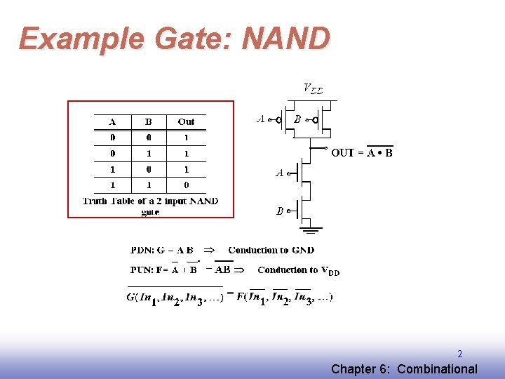
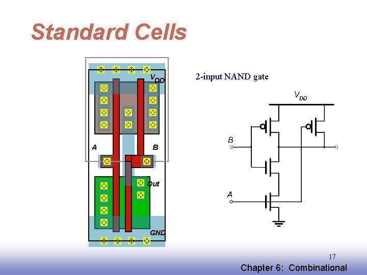
Example Gate: NAND 2 EE 141 Chapter 6: Combinational

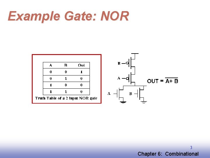
Example Gate: NOR 3 EE 141 Chapter 6: Combinational

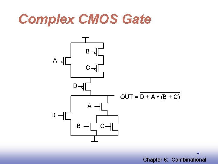
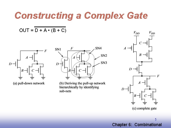
Complex CMOS Gate B A C D OUT = D + A • (B + C) A D B C 4 EE 141 Chapter 6: Combinational

Constructing a Complex Gate OUT = D + A • (B + C) 5 EE 141 Chapter 6: Combinational

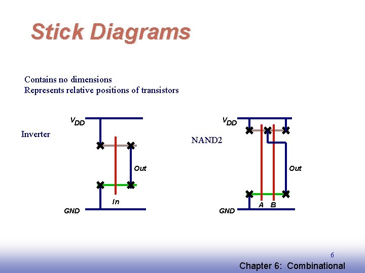
Stick Diagrams Contains no dimensions Represents relative positions of transistors VDD Inverter NAND 2 Out In GND A B 6 EE 141 Chapter 6: Combinational

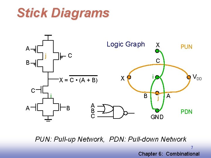
Stick Diagrams Logic Graph A j X C C B X = C • (A + B) C A i i X B B PUN A B C VDD j GND A PDN PUN: Pull-up Network, PDN: Pull-down Network 7 EE 141 Chapter 6: Combinational

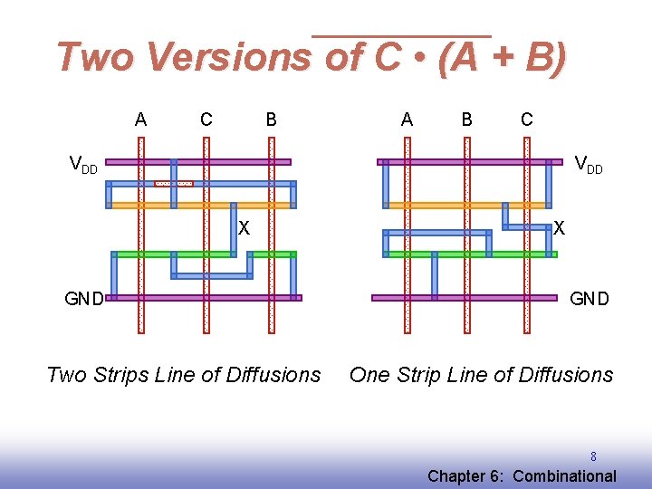
Two Versions of C • (A + B) A C B A B C VDD X GND Two Strips Line of Diffusions X GND One Strip Line of Diffusions 8 EE 141 Chapter 6: Combinational

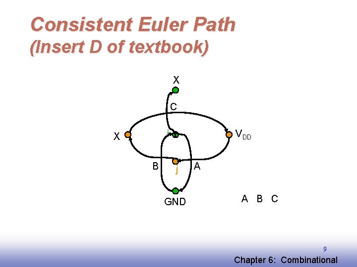
Consistent Euler Path (Insert D of textbook) X C i X B VDD j GND A A B C 9 EE 141 Chapter 6: Combinational

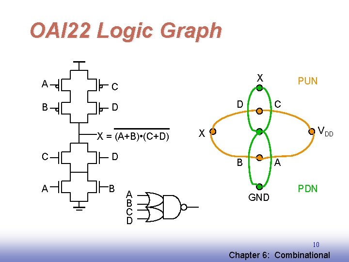
OAI 22 Logic Graph A C B D X = (A+B) • (C+D) C D A B C VDD X B A B C D PUN A GND PDN 10 EE 141 Chapter 6: Combinational

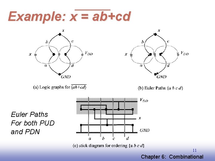
Example: x = ab+cd Euler Paths For both PUD and PDN 11 EE 141 Chapter 6: Combinational

Cell Design q Standard Cells (gate collection) § General purpose logic § Can be synthesized § Same height, varying width q Datapath Cells § For regular, structured designs (arithmetic) § Includes some wiring in the cell § Fixed height and width 12 EE 141 Chapter 6: Combinational

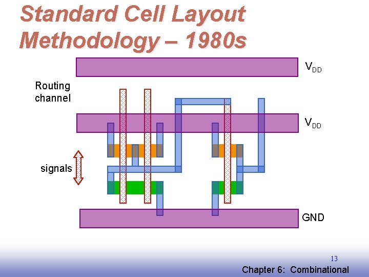
Standard Cell Layout Methodology – 1980 s VDD Routing channel VDD signals GND 13 EE 141 Chapter 6: Combinational

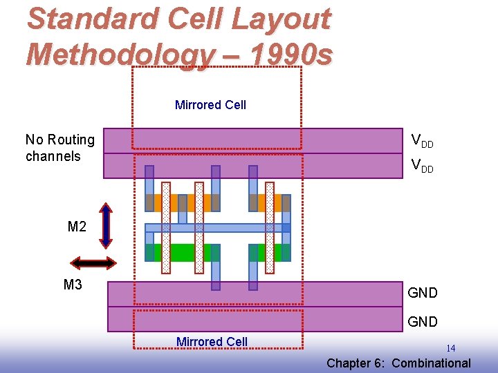
Standard Cell Layout Methodology – 1990 s Mirrored Cell No Routing channels VDD M 2 M 3 GND Mirrored Cell EE 141 14 Chapter 6: Combinational

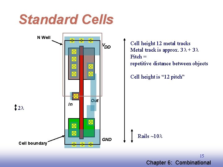
Standard Cells N Well VDD Cell height 12 metal tracks Metal track is approx. 3 + 3 Pitch = repetitive distance between objects Cell height is “ 12 pitch” 2 Cell boundary In Out GND Rails ~10 15 EE 141 Chapter 6: Combinational

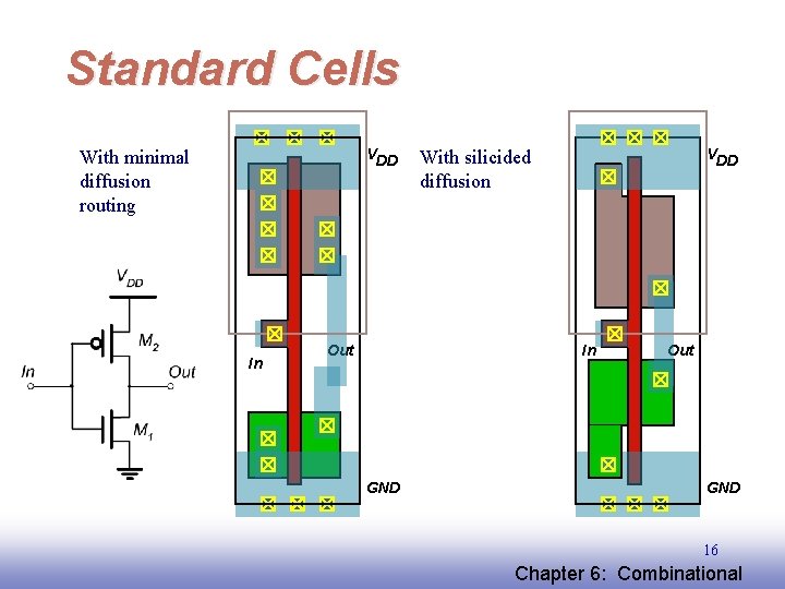
Standard Cells VDD With minimal diffusion routing In Out VDD With silicided diffusion In GND Out GND 16 EE 141 Chapter 6: Combinational

Standard Cells VDD A 2 -input NAND gate B Out GND 17 EE 141 Chapter 6: Combinational