
Power Management Integrated Circuits By Tai Nguyen Introduction
Power Management Integrated Circuits By Tai Nguyen
Introduction: What is a PMIC • Power Management Integrated Circuit • They are solid state devices that control the electrical power flow. • Voltage Regulators, DC-DC converters, LED/motor drivers, Battery chargers, AC to DC converters • On our 3 Do. T board, we have a boost converter (TPS 61200), MIC 5219 LDO, and the TB 6612 FNG dual motor driver. • Applications: • • Voltage regulation DC to DC conversion Load Switching Voltage protection
Voltage Regulators • Voltage regulators are devices that maintain a constant voltage level. They have a fixed output that won’t change, regardless of changes in the input voltage. • Voltage regulators are used in electronic devices in which excessive variations in voltage would be detrimental. • If you know you need a steady, constant voltage, use a voltage regulator. • Voltage regulators usually come in 2 types: linear and switching Sources: https: //www. jameco. com/Jameco/workshop/learning-center/voltage-regulator. html http: //www. analog. com/en/technical-articles/how-voltage-regulator-works. html
Linear Regulators • Linear regulators work by automatically adjusting the resistance via a feedback loop, accounting for both changes in the input and load to keep a constant output voltage. • Linear voltages can only step down, so the input voltage must always be higher than the output voltage. • They will tend to have lower efficiency because they output so much waste heat. Efficiency improves as the difference between the input and output voltage decreases. • Little noise in the output, for a clean DC output • A linear regulator regulates the output voltage by continually dissipating power in the pass transistor
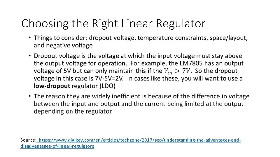
Choosing the Right Linear Regulator • Source: https: //www. digikey. com/en/articles/techzone/2017/sep/understanding-the-advantages-anddisadvantages-of-linear-regulators
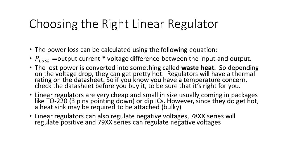
Choosing the Right Linear Regulator •
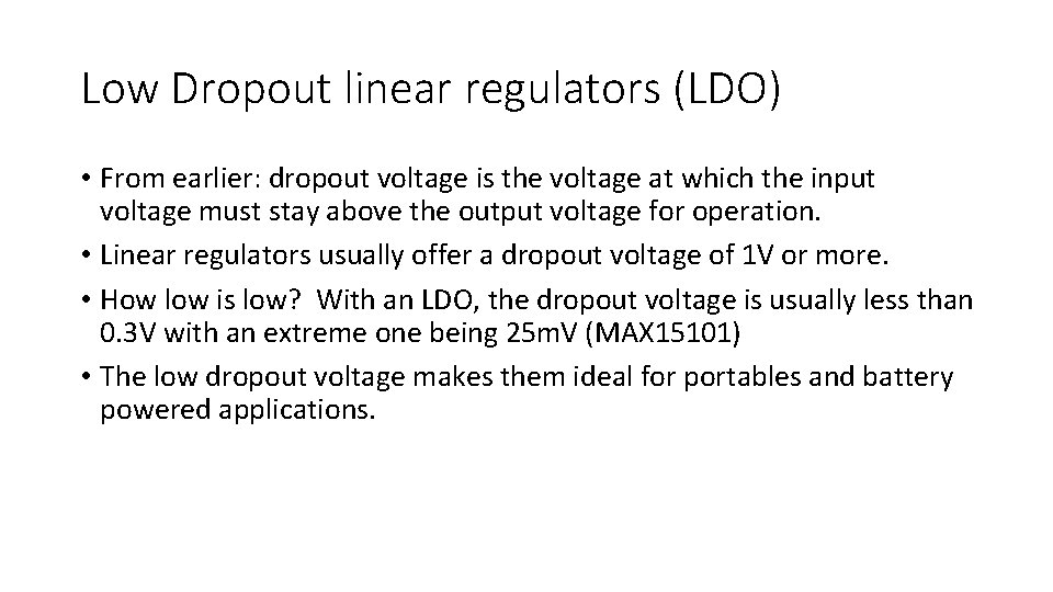
Low Dropout linear regulators (LDO) • From earlier: dropout voltage is the voltage at which the input voltage must stay above the output voltage for operation. • Linear regulators usually offer a dropout voltage of 1 V or more. • How low is low? With an LDO, the dropout voltage is usually less than 0. 3 V with an extreme one being 25 m. V (MAX 15101) • The low dropout voltage makes them ideal for portables and battery powered applications.
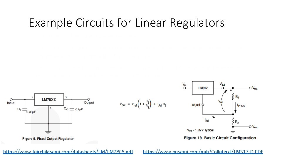
Example Circuits for Linear Regulators • https: //www. fairchildsemi. com/datasheets/LM/LM 7805. pdf https: //www. onsemi. com/pub/Collateral/LM 317 -D. PDF
Switching Regulators • Switching regulators use the pass transistor of a switching-mode supply to continually switch between low-dissipation, full-on and full-off states, and spends very little time in the high dissipation transitions, which minimizes wasted energy. • Voltage regulation is achieved by varying the ratio between on-to-off times. • Switching regulators advantage is higher power conversion efficiency. Ideally switching regulators dissipate no power. • There are still losses, specifically when the regulator switches between the on and off cycles. Power loss can be attributed to many things such as architecture (inductor core, capacitor choice, load), input voltage, output load conditions. • General rule of thumb, if your linear regulator is dissipating several watts of power, use a switching regulator instead Source: https: //www. dimensionengineering. com/info/switching-regulators
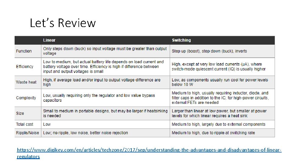
Let’s Review https: //www. digikey. com/en/articles/techzone/2017/sep/understanding-the-advantages-and-disadvantages-of-linearregulators
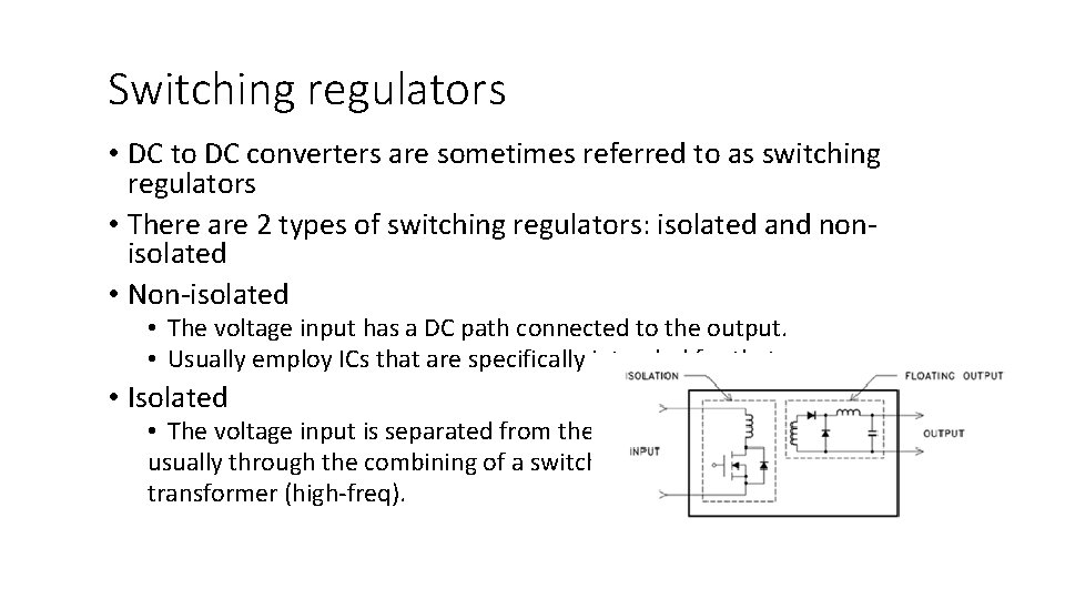
Switching regulators • DC to DC converters are sometimes referred to as switching regulators • There are 2 types of switching regulators: isolated and nonisolated • Non-isolated • The voltage input has a DC path connected to the output. • Usually employ ICs that are specifically intended for that purpose. • Isolated • The voltage input is separated from the output usually through the combining of a switch and a transformer (high-freq).
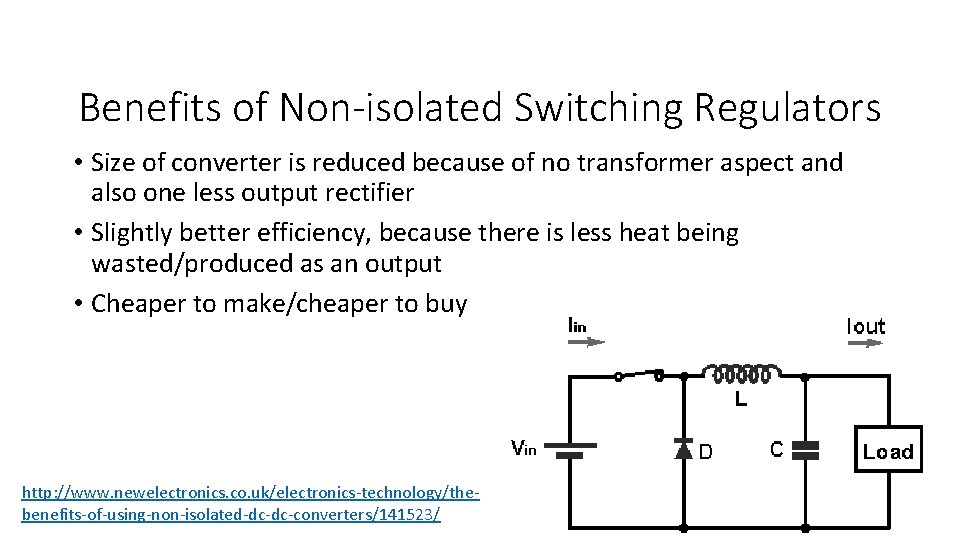
Benefits of Non-isolated Switching Regulators • Size of converter is reduced because of no transformer aspect and also one less output rectifier • Slightly better efficiency, because there is less heat being wasted/produced as an output • Cheaper to make/cheaper to buy http: //www. newelectronics. co. uk/electronics-technology/thebenefits-of-using-non-isolated-dc-dc-converters/141523/
Benefits of Isolated Switching Regulators • Number 1 Reason: Safety. The high frequency transformer will provide your output load with an electrical barrier in the case of an internal failure with your circuit • The barrier can be good for even thousands of volts • Output can be configured to either positive or negative depending on how you set up your positive and negative terminals • They have strong noise and interference blocking capability thus provide the load with a cleaner DC source which is required by many sensitive loads. https: //www. edn. com/electronics-blogs/power-supply-notes/4401305/Isolated---non-isolated-DC-DC-converters
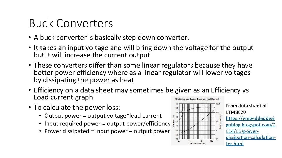
Buck Converters • A buck converter is basically step down converter. • It takes an input voltage and will bring down the voltage for the output but it will increase the current output • These converters differ than some linear regulators because they have better power efficiency where as a linear regulator will lower voltages by dissipating the power as heat • Efficiency on a data sheet may sometimes be given as an Efficiency vs Load current graph From data sheet of • To calculate the power loss: • Output power = output voltage*load current • Input required power = output power/efficiency • Power dissipated = input power – output power LTM 8020 https: //embeddeddesi gnblogspot. com/2 014/06/powerdissipation-calculationfor. html
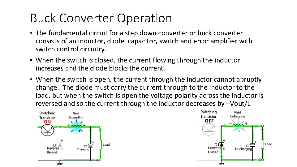
Buck Converter Operation • The fundamental circuit for a step down converter or buck converter consists of an inductor, diode, capacitor, switch and error amplifier with switch control circuitry. • When the switch is closed, the current flowing through the inductor increases and the diode blocks the current. • When the switch is open, the current through the inductor cannot abruptly change. The diode must carry the current through to the inductor to the load, but when the switch is open the voltage polarity across the inductor is reversed and so the current through the inductor decreases by –Vout/L
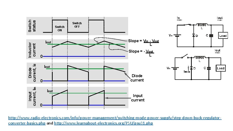
http: //www. radio-electronics. com/info/power-management/switching-mode-power-supply/step-down-buck-regulatorconverter-basics. php and http: //www. learnabout-electronics. org/PSU/psu 31. php
Boost Converters • The opposite of a buck converter. These will increase/step-up your voltage but will also reduce the current. So the same equation as before still applies: • Input Voltage x Input Current = Output Voltage x Output Current • An application for a Boost converter would be if your board is running at 3. 3 V, but you have a servo/motor in your circuit that needs a 5 V input to run it. You would include a boost converter to step up the voltage and power the motor. • A good example for a Boost Converter is the TPS 61253 • Wide input voltage range 2. 3 -5. 5 V • 93% efficiency at 3. 5 MHz operation • Iout is approximately 800 m. A (most likely will be good enough for whatever you’ll be trying to power) • Overload protection with option for load disconnect during shutdown
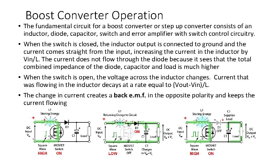
Boost Converter Operation • The fundamental circuit for a boost converter or step up converter consists of an inductor, diode, capacitor, switch and error amplifier with switch control circuitry. • When the switch is closed, the inductor output is connected to ground and the current comes straight from the input, increasing the current in the inductor by Vin/L. The current does not flow through the diode because it sees that the total combined impedance of the diode, capacitor and load is much higher • When the switch is open, the voltage across the inductor changes. Current that was flowing in the inductor decays at a rate equal to (Vout-Vin)/L. • The change in current creates a back e. m. f. in the opposite polarity and keeps the current flowing
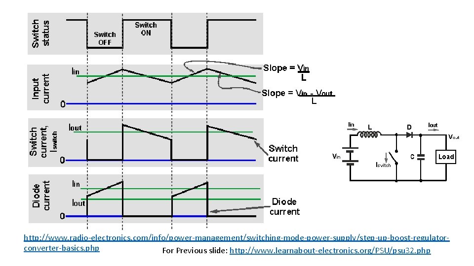
http: //www. radio-electronics. com/info/power-management/switching-mode-power-supply/step-up-boost-regulatorconverter-basics. php For Previous slide: http: //www. learnabout-electronics. org/PSU/psu 32. php
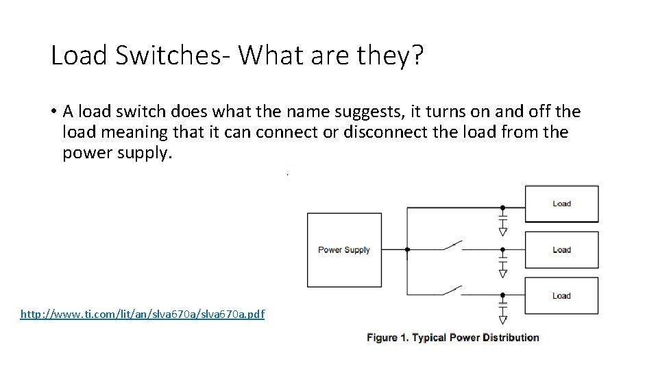
Load Switches- What are they? • A load switch does what the name suggests, it turns on and off the load meaning that it can connect or disconnect the load from the power supply. http: //www. ti. com/lit/an/slva 670 a. pdf
Load Switches – What can I do with them? • By disconnecting power to a load, when it is not being used, less power is used in the system. • Load switches can be used to control inrush current. Inrush current occurs when a switch first turns on, there can be a very large surge/spike of current through the system. Load switching can be used to control this current often called slew rate control. • Slew rate is the change in voltage over time, how fast the supply voltage transfers power to the load. • When a power supply has a multiple loads to power at the same time, there is a lot of stress on the supply. Load switching can be used to instead to turn on the loads one at a time.
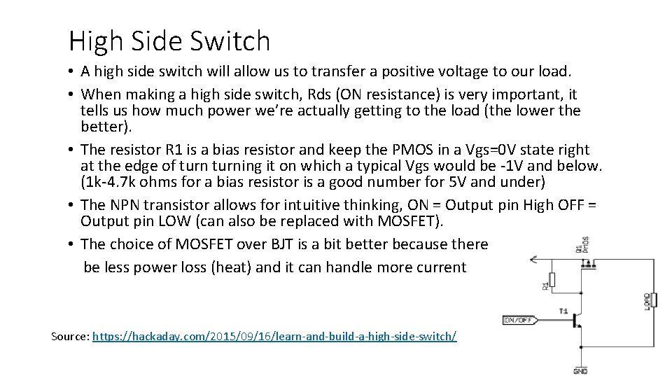
High Side Switch • A high side switch will allow us to transfer a positive voltage to our load. • When making a high side switch, Rds (ON resistance) is very important, it tells us how much power we’re actually getting to the load (the lower the better). • The resistor R 1 is a bias resistor and keep the PMOS in a Vgs=0 V state right at the edge of turning it on which a typical Vgs would be -1 V and below. (1 k-4. 7 k ohms for a bias resistor is a good number for 5 V and under) • The NPN transistor allows for intuitive thinking, ON = Output pin High OFF = Output pin LOW (can also be replaced with MOSFET). • The choice of MOSFET over BJT is a bit better because there will be less power loss (heat) and it can handle more current Source: https: //hackaday. com/2015/09/16/learn-and-build-a-high-side-switch/
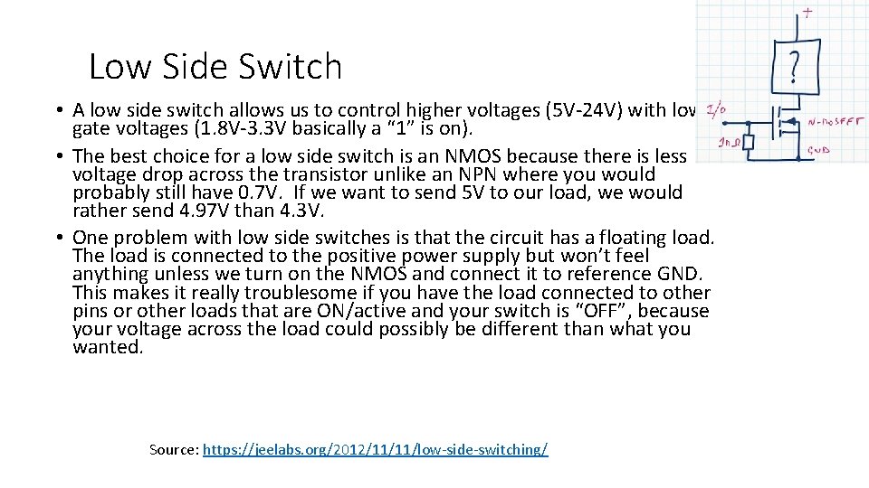
Low Side Switch • A low side switch allows us to control higher voltages (5 V-24 V) with low gate voltages (1. 8 V-3. 3 V basically a “ 1” is on). • The best choice for a low side switch is an NMOS because there is less voltage drop across the transistor unlike an NPN where you would probably still have 0. 7 V. If we want to send 5 V to our load, we would rather send 4. 97 V than 4. 3 V. • One problem with low side switches is that the circuit has a floating load. The load is connected to the positive power supply but won’t feel anything unless we turn on the NMOS and connect it to reference GND. This makes it really troublesome if you have the load connected to other pins or other loads that are ON/active and your switch is “OFF”, because your voltage across the load could possibly be different than what you wanted. Source: https: //jeelabs. org/2012/11/11/low-side-switching/
What’s the difference • It may seem like both perform the exact same duty of switching on a load, but if there wasn’t a difference, there wouldn’t be a need to differentiate the two. • P-Channel MOSFETs use “holes” as their carriers unlike the NChannel MOSFET which uses electrons. • “The simplest statement is that hole mobility is less than electron mobility. ” • Because of this NMOS typically have lower ON resistances than a PMOS does • High side switch – safety, can use the same ground for connecting multiple loads • Low side switch – easy to configure and convenient
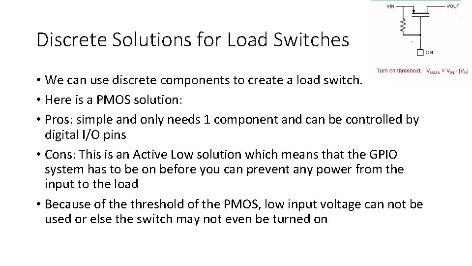
Discrete Solutions for Load Switches • We can use discrete components to create a load switch. • Here is a PMOS solution: • Pros: simple and only needs 1 component and can be controlled by digital I/O pins • Cons: This is an Active Low solution which means that the GPIO system has to be on before you can prevent any power from the input to the load • Because of the threshold of the PMOS, low input voltage can not be used or else the switch may not even be turned on
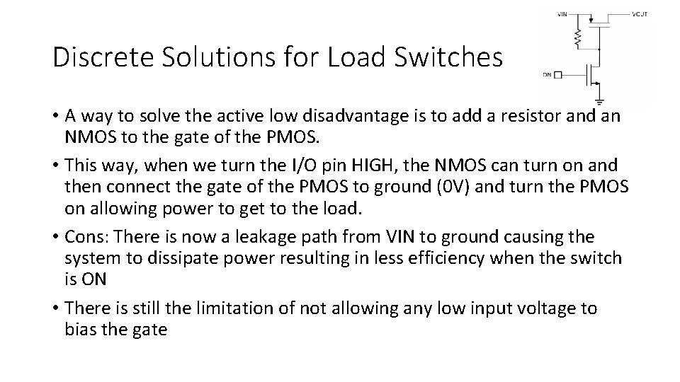
Discrete Solutions for Load Switches • A way to solve the active low disadvantage is to add a resistor and an NMOS to the gate of the PMOS. • This way, when we turn the I/O pin HIGH, the NMOS can turn on and then connect the gate of the PMOS to ground (0 V) and turn the PMOS on allowing power to get to the load. • Cons: There is now a leakage path from VIN to ground causing the system to dissipate power resulting in less efficiency when the switch is ON • There is still the limitation of not allowing any low input voltage to bias the gate
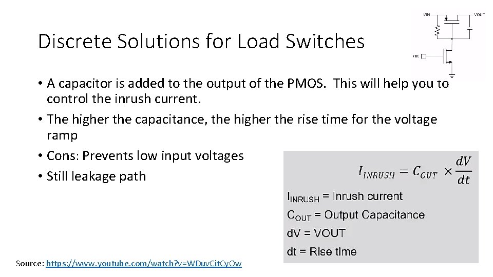
Discrete Solutions for Load Switches • A capacitor is added to the output of the PMOS. This will help you to control the inrush current. • The higher the capacitance, the higher the rise time for the voltage ramp • Cons: Prevents low input voltages • Still leakage path Source: https: //www. youtube. com/watch? v=WDuv. Cit. Cy. Ow
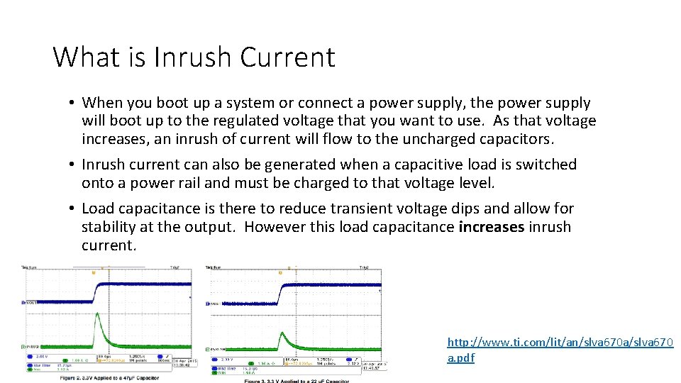
What is Inrush Current • When you boot up a system or connect a power supply, the power supply will boot up to the regulated voltage that you want to use. As that voltage increases, an inrush of current will flow to the uncharged capacitors. • Inrush current can also be generated when a capacitive load is switched onto a power rail and must be charged to that voltage level. • Load capacitance is there to reduce transient voltage dips and allow for stability at the output. However this load capacitance increases inrush current. http: //www. ti. com/lit/an/slva 670 a/slva 670 a. pdf
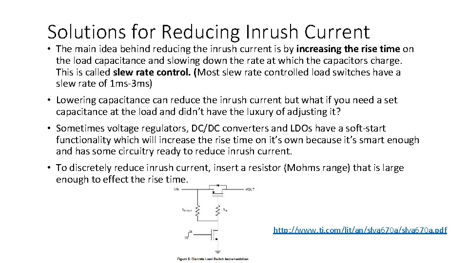
Solutions for Reducing Inrush Current • The main idea behind reducing the inrush current is by increasing the rise time on the load capacitance and slowing down the rate at which the capacitors charge. This is called slew rate control. (Most slew rate controlled load switches have a slew rate of 1 ms-3 ms) • Lowering capacitance can reduce the inrush current but what if you need a set capacitance at the load and didn’t have the luxury of adjusting it? • Sometimes voltage regulators, DC/DC converters and LDOs have a soft-start functionality which will increase the rise time on it’s own because it’s smart enough and has some circuitry ready to reduce inrush current. • To discretely reduce inrush current, insert a resistor (Mohms range) that is large enough to effect the rise time. http: //www. ti. com/lit/an/slva 670 a. pdf
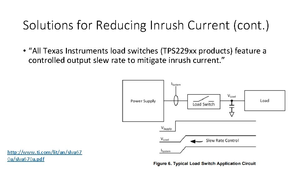
Solutions for Reducing Inrush Current (cont. ) • “All Texas Instruments load switches (TPS 229 xx products) feature a controlled output slew rate to mitigate inrush current. ” http: //www. ti. com/lit/an/slva 67 0 a/slva 670 a. pdf
Quick Output Discharge (QOD) • Even though you may have your circuit correctly wired for the switch to be off when the I/O pin is LOW, when you apply your VIN for the first time, there is a moment where the PMOS allows voltage and current through the switch. This can be caused by things like battery insertion or initial system start up. • When you apply VIN, the capacitor is slowly charging the gate and the switch isn’t fully turned off even though it should be. • A solution to prevent this will be to include QOD will pull down the output of the switch to 0 V when the switch is turned off. • Discharge circuit is very good in digital electronics because they hate the slow ramp of turning something off. This way, you can take all the stored charge and send it to ground and the load sees 0 V
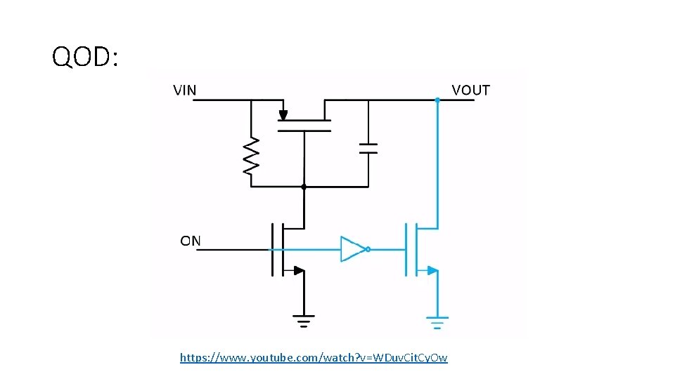
QOD: https: //www. youtube. com/watch? v=WDuv. Cit. Cy. Ow
The PMOS- EE 330 Review • The PMOS says that in order for it to be ON, the VGS has to be a negative and not just negative, more negative than that of the threshold. • We can use a PMOS to give us a way to implement reverse voltage protection • By putting in a PMOS into a circuit in between the input and the load, if the polarity of the input is backwards, the current will be blocked off to the load and the load is protected • When putting in a MOSFET we have to check out the Rds of the package. The higher the Rds the more power we lose out on and less efficiency we get from our input
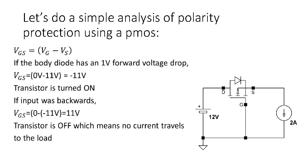
Let’s do a simple analysis of polarity protection using a pmos: •
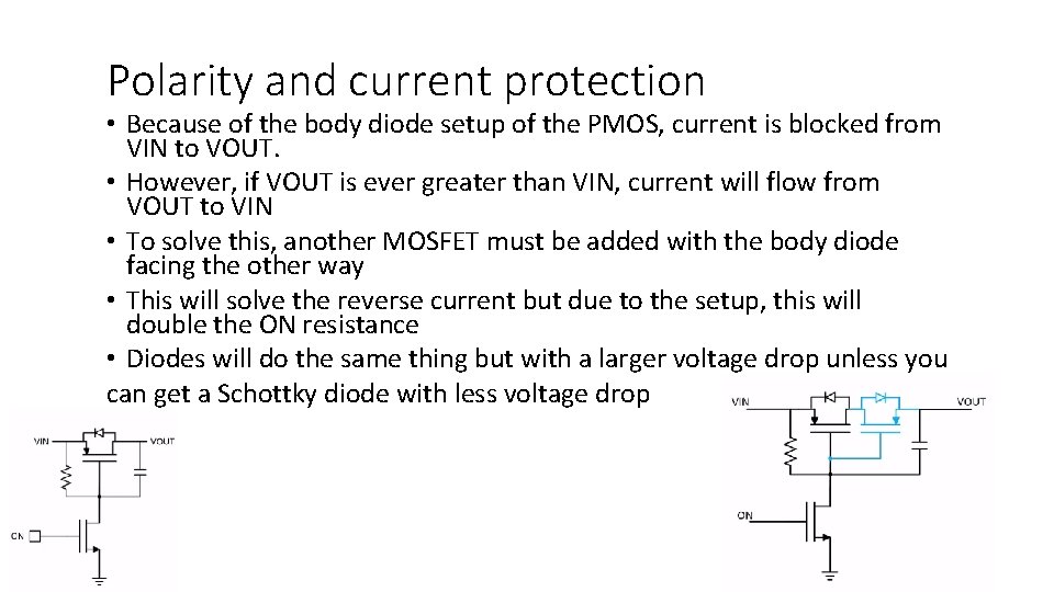
Polarity and current protection • Because of the body diode setup of the PMOS, current is blocked from VIN to VOUT. • However, if VOUT is ever greater than VIN, current will flow from VOUT to VIN • To solve this, another MOSFET must be added with the body diode facing the other way • This will solve the reverse current but due to the setup, this will double the ON resistance • Diodes will do the same thing but with a larger voltage drop unless you can get a Schottky diode with less voltage drop
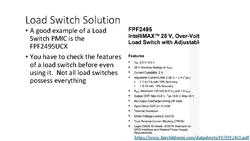
Load Switch Solution • A good example of a Load Switch PMIC is the FPF 2495 UCX • You have to check the features of a load switch before even using it. Not all load switches possess everything https: //www. fairchildsemi. com/datasheets/FP/FPF 2495. pdf
Questions? • Check for comprehension. • End of Power. Point • Move to MC questions.
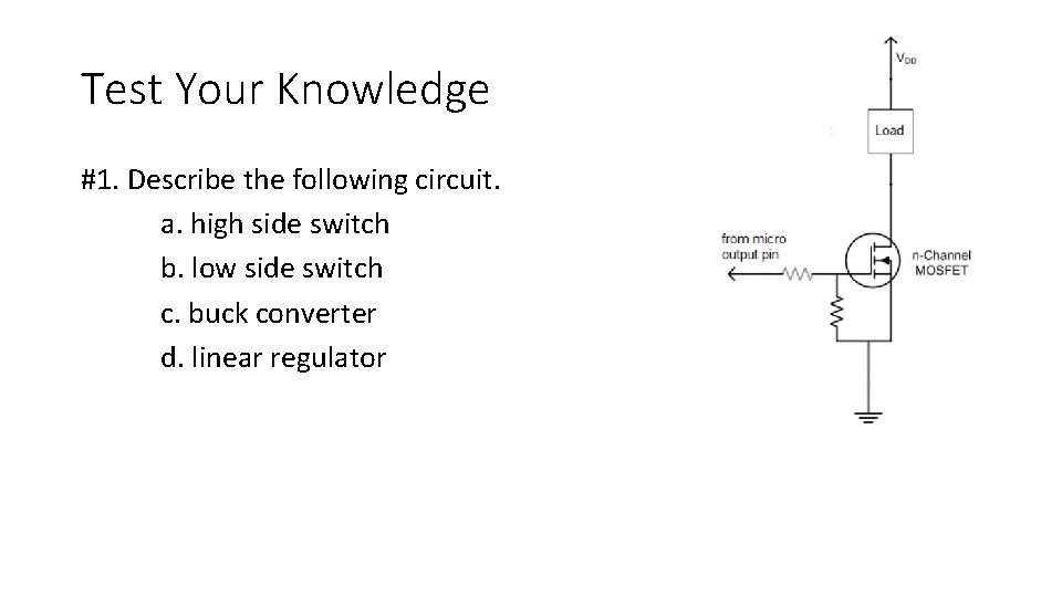
Test Your Knowledge #1. Describe the following circuit. a. high side switch b. low side switch c. buck converter d. linear regulator
• #2. Which is a solution are there to reduce inrush current? a. Increase the input capacitance so that the slew rate increases because the supply has to charge the capacitor b. Add a large resistance at the gate of the transistor switch c. Increase the rise time by adding more load capacitance for higher slew rate during the transient response d. Insert a transistor so that it’s back to back with the load switch transistor to increase the ON resistance
• #3. Which of the following can a load switch be used for? a. b. c. d. Disconnecting loads to the power supply Control inrush current Turning on loads one at a time All the above
• #4. What can a PMIC be used for? Choose all that apply. a. b. c. d. Load Switching Voltage Protection DC to DC conversion Voltage regulation
• #5 What is the main difference between an isolated DC to DC converter and a non-isolated one? a. The switch on an isolated DC to DC converter is mechanical b. Non isolated converters have one more output rectifier in the circuit c. The output on an isolated converter has no electrical connection to the input d. Non isolated converters can produce negative voltages
• #6. What is the benefit of non-isolated DC to DC converters? a. b. c. d. Better efficiency for bigger size compared to isolated More components for better circuit protection Safer to use by design Cheaper and smaller because less components
#7. What is the difference between linear regulators and switching regulators? a. Linear regulators are more efficient than switching regulators b. Switching regulators produce a lot of waste heat compared to linear regulators c. Switching regulators have a larger voltage conversion range d. Linear regulators are less efficient than switching regulators
#8. How does a boost converter use an inductor’s stored energy to step up voltage? a. the inductor’s energy will release, opening the switch to the diode that will allow current to flow to the load b. the inductor will release the stored energy to the capacitor when the switch has been opened and the capacitor will transfer all the voltage to the load c. The inductor will release the stored energy to the capacitor when the switch has been closed and then in the next open cycle, the capacitor will then transfer the energy stored to the load d. the diode will allow current to pass through to the inductor and the inductor will overflow with current and release energy to the load
#9 What does QOD stand for? a. b. c. d. Quick Output Dissipation Quick Output Discharge Quick Output Direction Quick Output Deregulator
#10. What should you be aware of when creating a load switch from discrete components? a. Inrush current b. QOD c. Reverse Current blocking d. Power efficiency e. All the above
Answers 1. B 2. B 3. D 4. A, B, C, D 5. C 6. C 7. D 8. C 9. B 10. E
- Slides: 48