1 Chapter 4 MOS FieldEffect Transistors MOSFETs 202215
- Slides: 84

1 Chapter 4 MOS Field-Effect Transistors (MOSFETs) 2022/1/5 J. Chen

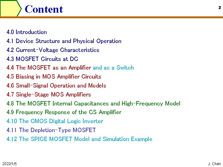
Content 2 4. 0 Introduction 4. 1 Device Structure and Physical Operation 4. 2 Current-Voltage Characteristics 4. 3 MOSFET Circuits at DC 4. 4 The MOSFET as an Amplifier and as a Switch 4. 5 Biasing in MOS Amplifier Circuits 4. 6 Small-Signal Operation and Models 4. 7 Single-Stage MOS Amplifiers 4. 8 The MOSFET Internal Capacitances and High-Frequency Model 4. 9 Frequency Response of the CS Amplifier 4. 10 The CMOS Digital Logic Inverter 4. 11 The Depletion-Type MOSFET 4. 12 The SPICE MOSFET Model and Simulation Example 2022/1/5 J. Chen

4. 0 Introduction to FET l Three-terminal devices are far more useful than two-terminal ones, because they can be used in a multitude of applications, Ø Ø l 3 signal amplification digital logic memory circuits. …… The basic principle the use of the voltage between two terminals to control the current flowing in the third terminal. Ø 2022/1/5 Transistor = transfer resistor J. P. Chen

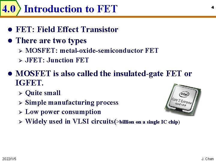
4. 0 Introduction to FET 4 FET: Field Effect Transistor l There are two types l Ø Ø l MOSFET: metal-oxide-semiconductor FET JFET: Junction FET MOSFET is also called the insulated-gate FET or IGFET. Ø Ø 2022/1/5 Quite small Simple manufacturing process Low power consumption Widely used in VLSI circuits(>billion on a single IC chip) J. Chen

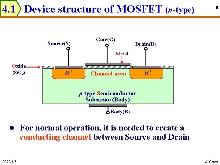
4. 1 Device structure of MOSFET (n-type) Source(S) Gate(G) 5 Drain(D) Metal Oxide (Si. O 2) n+ Channel area n+ p-type Semiconductor Substrate (Body) Body(B) l 2022/1/5 For normal operation, it is needed to create a conducting channel between Source and Drain J. Chen

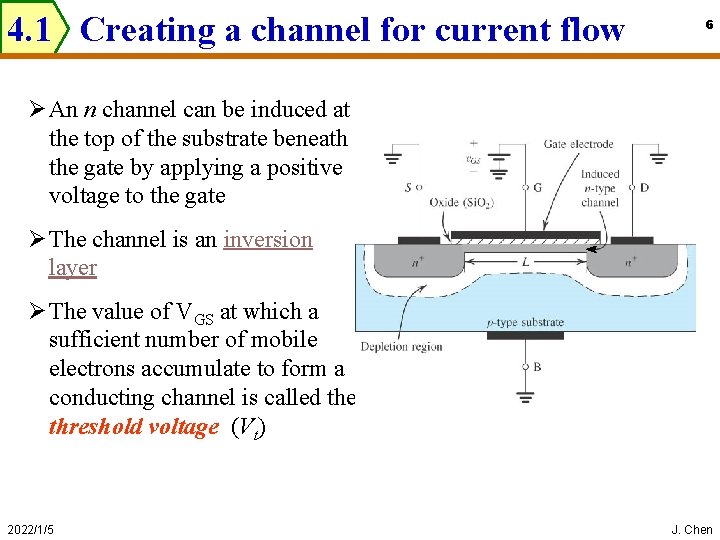
4. 1 Creating a channel for current flow 6 Ø An n channel can be induced at the top of the substrate beneath the gate by applying a positive voltage to the gate Ø The channel is an inversion layer Ø The value of VGS at which a sufficient number of mobile electrons accumulate to form a conducting channel is called the threshold voltage (Vt) 2022/1/5 J. Chen

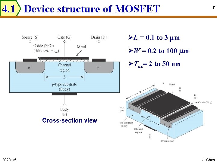
4. 1 Device structure of MOSFET 7 ØL = 0. 1 to 3 mm ØW = 0. 2 to 100 mm ØTox= 2 to 50 nm Cross-section view 2022/1/5 J. Chen

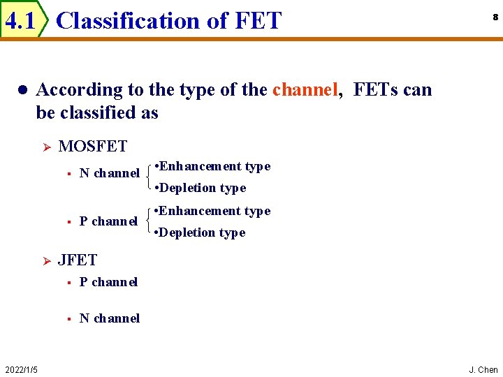
4. 1 Classification of FET l 8 According to the type of the channel, FETs can be classified as Ø MOSFET § § Ø 2022/1/5 N channel P channel • Enhancement type • Depletion type JFET § P channel § N channel J. Chen

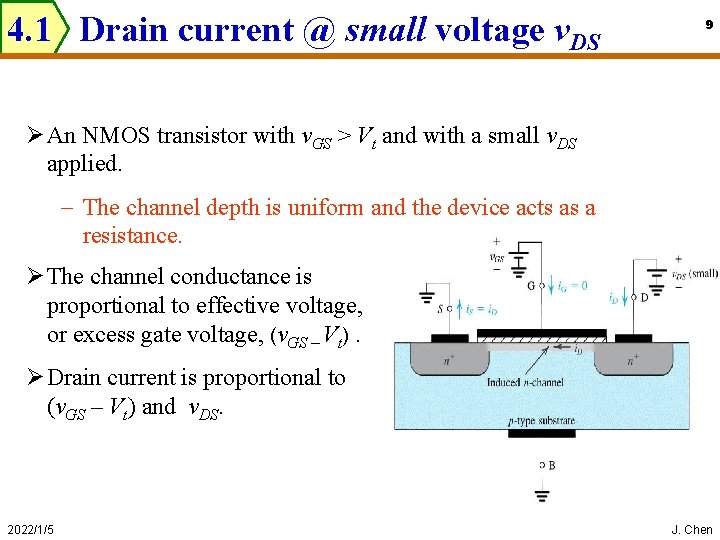
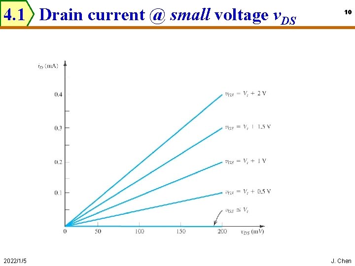
4. 1 Drain current @ small voltage v. DS 9 Ø An NMOS transistor with v. GS > Vt and with a small v. DS applied. - The channel depth is uniform and the device acts as a resistance. Ø The channel conductance is proportional to effective voltage, or excess gate voltage, (v. GS – Vt). Ø Drain current is proportional to (v. GS – Vt) and v. DS. 2022/1/5 J. Chen

4. 1 Drain current @ small voltage v. DS 2022/1/5 10 J. Chen

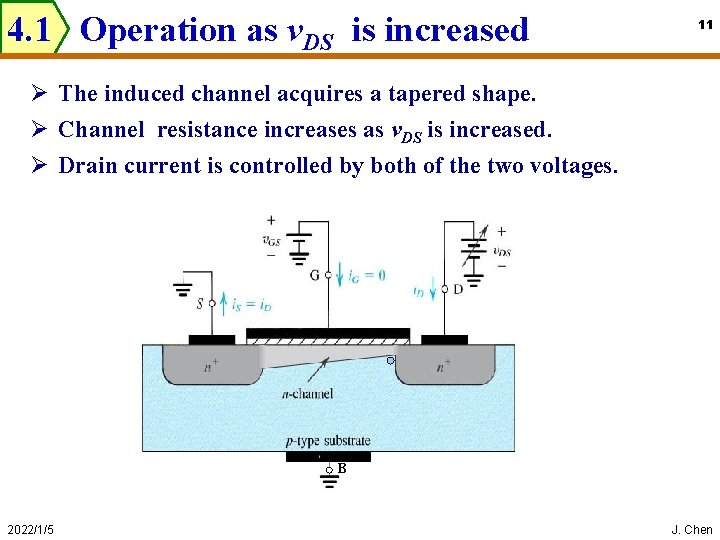
4. 1 Operation as v. DS is increased 11 Ø The induced channel acquires a tapered shape. Ø Channel resistance increases as v. DS is increased. Ø Drain current is controlled by both of the two voltages. B 2022/1/5 J. Chen

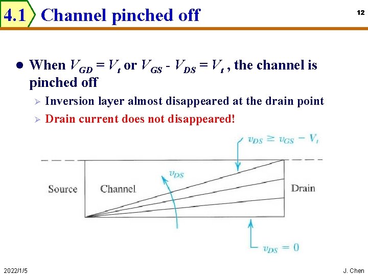
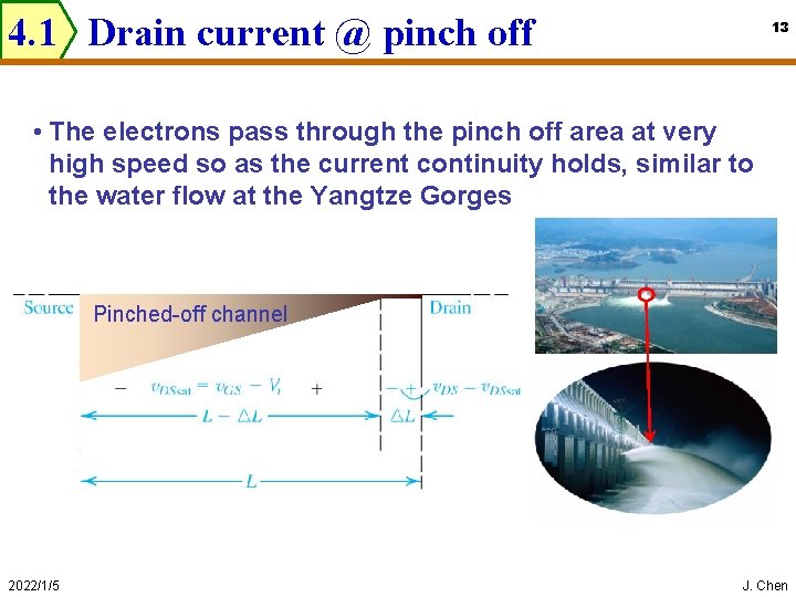
4. 1 Channel pinched off l When VGD = Vt or VGS - VDS = Vt , the channel is pinched off Ø Ø 2022/1/5 12 Inversion layer almost disappeared at the drain point Drain current does not disappeared! J. Chen

4. 1 Drain current @ pinch off 13 • The electrons pass through the pinch off area at very high speed so as the current continuity holds, similar to the water flow at the Yangtze Gorges Pinched-off channel 2022/1/5 J. Chen

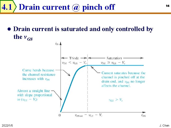
4. 1 Drain current @ pinch off l 2022/1/5 14 Drain current is saturated and only controlled by the v. GS J. Chen

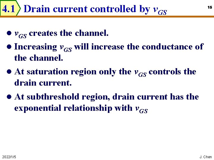
4. 1 Drain current controlled by v. GS 15 l v. GS creates the channel. l Increasing v. GS will increase the conductance of the channel. l At saturation region only the v. GS controls the drain current. l At subthreshold region, drain current has the exponential relationship with v. GS 2022/1/5 J. Chen

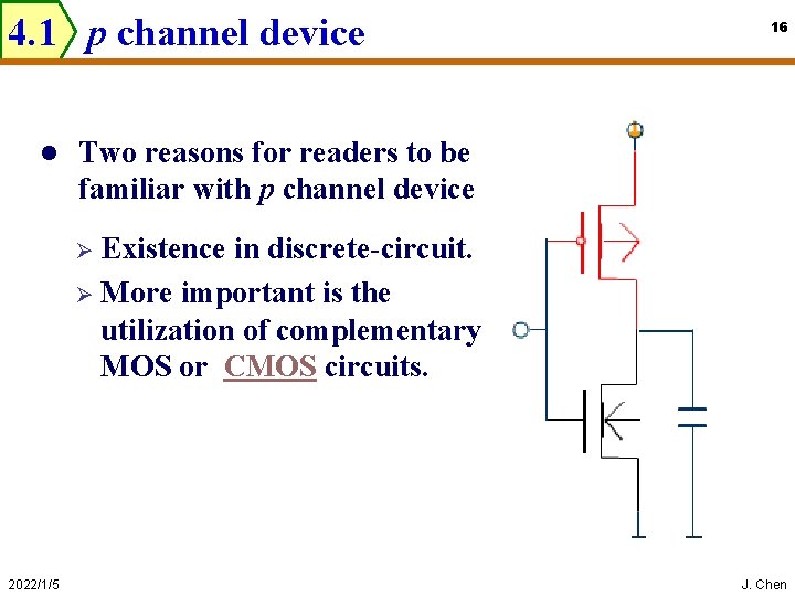
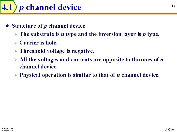
4. 1 p channel device l 16 Two reasons for readers to be familiar with p channel device Existence in discrete-circuit. Ø More important is the utilization of complementary MOS or CMOS circuits. Ø 2022/1/5 J. Chen

4. 1 p channel device l 17 Structure of p channel device Ø The substrate is n type and the inversion layer is p type. Ø Carrier is hole. Ø Threshold voltage is negative. Ø All the voltages and currents are opposite to the ones of n channel device. Ø Physical operation is similar to that of n channel device. 2022/1/5 J. Chen

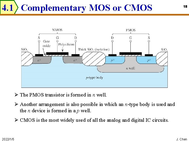
4. 1 Complementary MOS or CMOS 18 Ø The PMOS transistor is formed in n well. Ø Another arrangement is also possible in which an n-type body is used and the n device is formed in a p well. Ø CMOS is the most widely used of all the analog and digital IC circuits. 2022/1/5 J. Chen

4. 2 Current-voltage characteristics 19 l Circuit symbol l Output characteristic curves l Channel length modulation l Characteristics of p channel device l Body effect l Temperature effects and Breakdown Region 2022/1/5 J. Chen

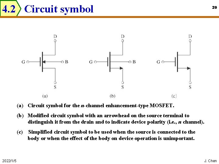
4. 2 Circuit symbol 20 (a) Circuit symbol for the n-channel enhancement-type MOSFET. (b) Modified circuit symbol with an arrowhead on the source terminal to distinguish it from the drain and to indicate device polarity (i. e. , n channel). (c) 2022/1/5 Simplified circuit symbol to be used when the source is connected to the body or when the effect of the body on device operation is unimportant. J. Chen

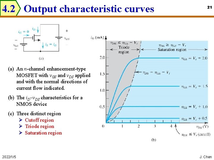
4. 2 Output characteristic curves 21 (a) An n-channel enhancement-type MOSFET with v. GS and v. DS applied and with the normal directions of current flow indicated. (b) The i. D–v. DS characteristics for a NMOS device (c) Three distinct region Ø Cutoff region Ø Triode region Ø Saturation region 2022/1/5 J. Chen

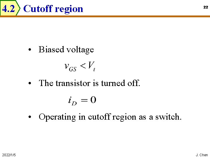
4. 2 Cutoff region 22 • Biased voltage • The transistor is turned off. • Operating in cutoff region as a switch. 2022/1/5 J. Chen

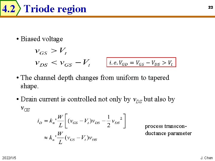
4. 2 Triode region 23 • Biased voltage • The channel depth changes from uniform to tapered shape. • Drain current is controlled not only by v. DS but also by v. GS process transconductance parameter 2022/1/5 J. Chen

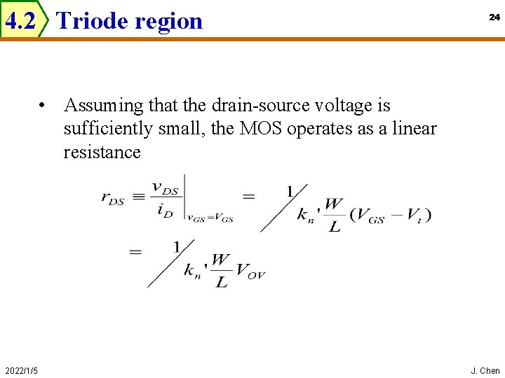
4. 2 Triode region 24 • Assuming that the drain-source voltage is sufficiently small, the MOS operates as a linear resistance 2022/1/5 J. Chen

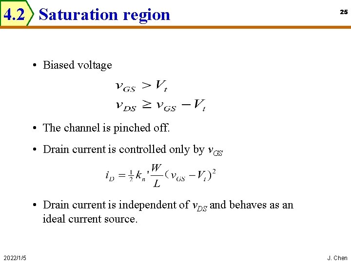
4. 2 Saturation region 25 • Biased voltage • The channel is pinched off. • Drain current is controlled only by v. GS • Drain current is independent of v. DS and behaves as an ideal current source. 2022/1/5 J. Chen

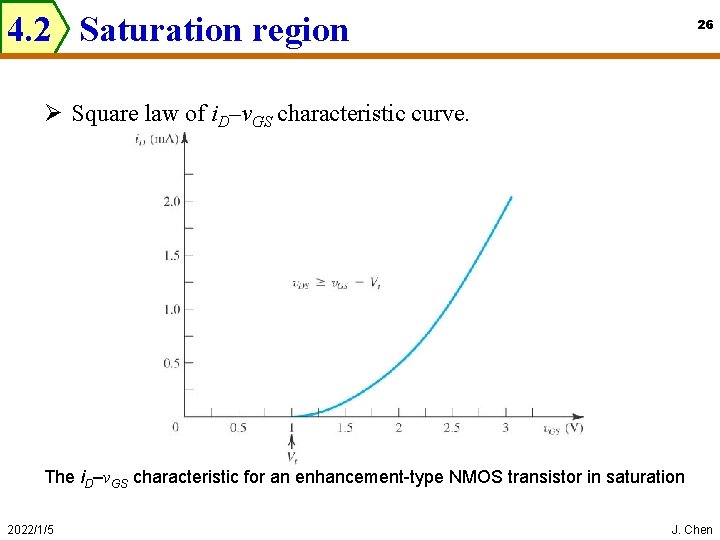
4. 2 Saturation region 26 Ø Square law of i. D–v. GS characteristic curve. The i. D–v. GS characteristic for an enhancement-type NMOS transistor in saturation 2022/1/5 J. Chen

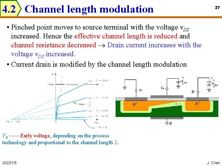
4. 2 Channel length modulation 27 • Pinched point moves to source terminal with the voltage v. DS increased. Hence the effective channel length is reduced and channel resistance decreased Drain current increases with the voltage v. DS increased. • Current drain is modified by the channel length modulation VA ——Early voltage, depending on the process technology and proportional to the channel length L. 2022/1/5 J. Chen

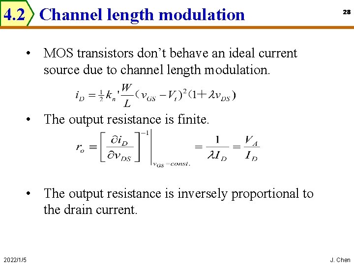
4. 2 Channel length modulation 28 • MOS transistors don’t behave an ideal current source due to channel length modulation. • The output resistance is finite. • The output resistance is inversely proportional to the drain current. 2022/1/5 J. Chen

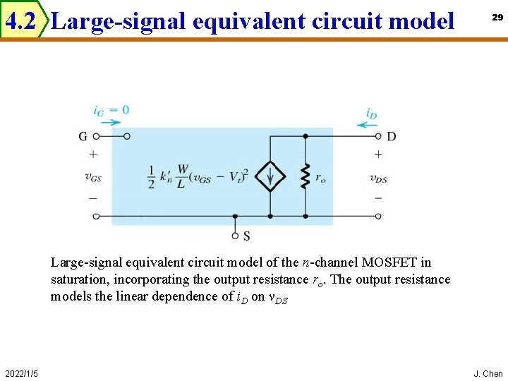
4. 2 Large-signal equivalent circuit model 29 Large-signal equivalent circuit model of the n-channel MOSFET in saturation, incorporating the output resistance ro. The output resistance models the linear dependence of i. D on v. DS 2022/1/5 J. Chen

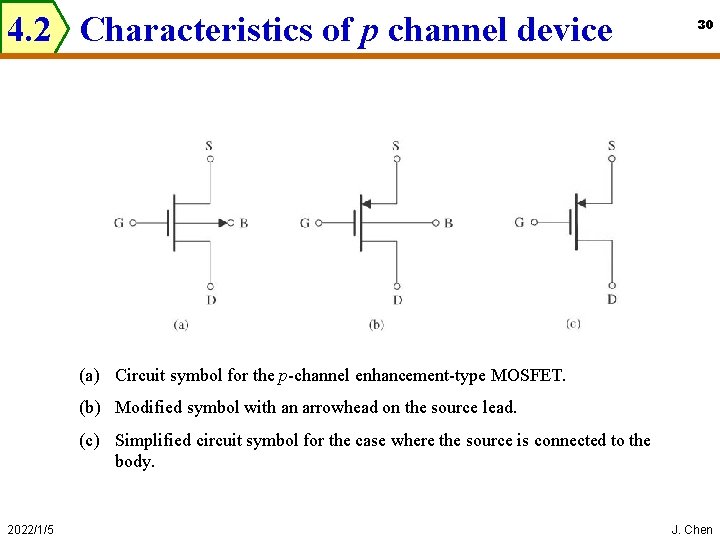
4. 2 Characteristics of p channel device 30 (a) Circuit symbol for the p-channel enhancement-type MOSFET. (b) Modified symbol with an arrowhead on the source lead. (c) Simplified circuit symbol for the case where the source is connected to the body. 2022/1/5 J. Chen

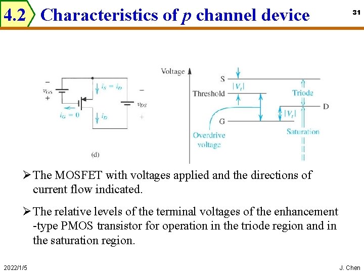
4. 2 Characteristics of p channel device 31 Ø The MOSFET with voltages applied and the directions of current flow indicated. Ø The relative levels of the terminal voltages of the enhancement -type PMOS transistor for operation in the triode region and in the saturation region. 2022/1/5 J. Chen

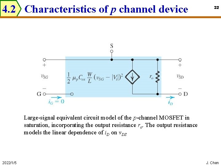
4. 2 Characteristics of p channel device 32 Large-signal equivalent circuit model of the p-channel MOSFET in saturation, incorporating the output resistance ro. The output resistance models the linear dependence of i. D on v. DS 2022/1/5 J. Chen

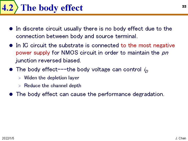
4. 2 The body effect 33 In discrete circuit usually there is no body effect due to the connection between body and source terminal. l In IC circuit the substrate is connected to the most negative power supply for NMOS circuit in order to maintain the pn junction reversed biased. l The body effect---the body voltage can control i. D l Ø Ø l 2022/1/5 Widen the depletion layer Reduce the channel depth The body effect can cause the performance degradation. J. Chen

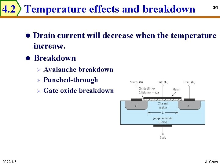
4. 2 Temperature effects and breakdown 34 Drain current will decrease when the temperature increase. l Breakdown l Ø Ø Ø 2022/1/5 Avalanche breakdown Punched-through Gate oxide breakdown J. Chen


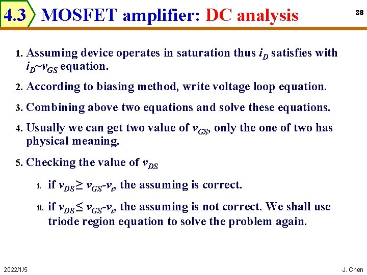
4. 3 MOSFET amplifier: DC analysis 1. Assuming device operates in saturation thus i. D satisfies with i. D~v. GS equation. 2. According to biasing method, write voltage loop equation. 3. Combining above two equations and solve these equations. 4. Usually we can get two value of v. GS, only the one of two has physical meaning. 5. Checking the value of v. DS 2022/1/5 i. if v. DS ≥ v. GS-vt, the assuming is correct. ii. if v. DS ≤ v. GS-vt, the assuming is not correct. We shall use triode region equation to solve the problem again. 38 J. Chen

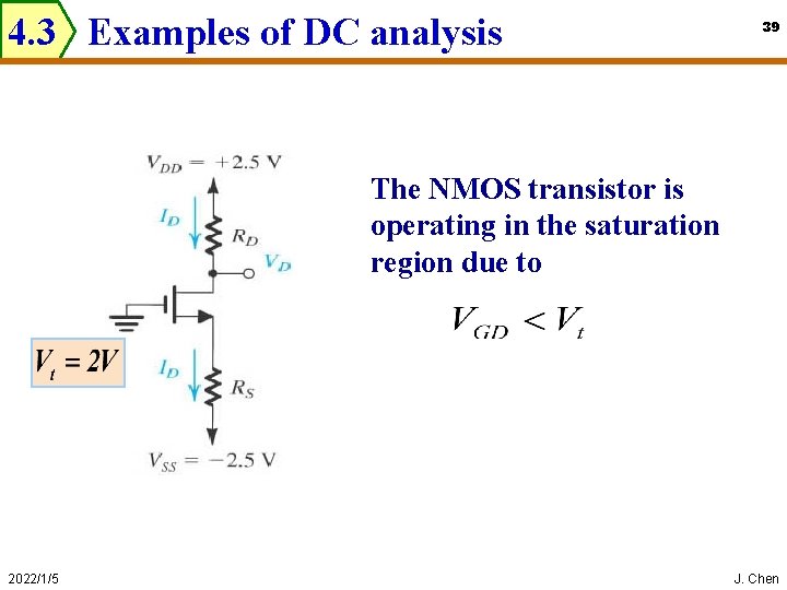
4. 3 Examples of DC analysis 39 The NMOS transistor is operating in the saturation region due to 2022/1/5 J. Chen

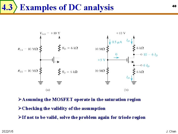
4. 3 Examples of DC analysis 40 ØAssuming the MOSFET operate in the saturation region ØChecking the validity of the assumption ØIf not to be valid, solve the problem again for triode region 2022/1/5 J. Chen

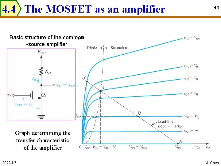
4. 4 The MOSFET as an amplifier 41 Basic structure of the common -source amplifier Graph determining the transfer characteristic of the amplifier 2022/1/5 J. Chen

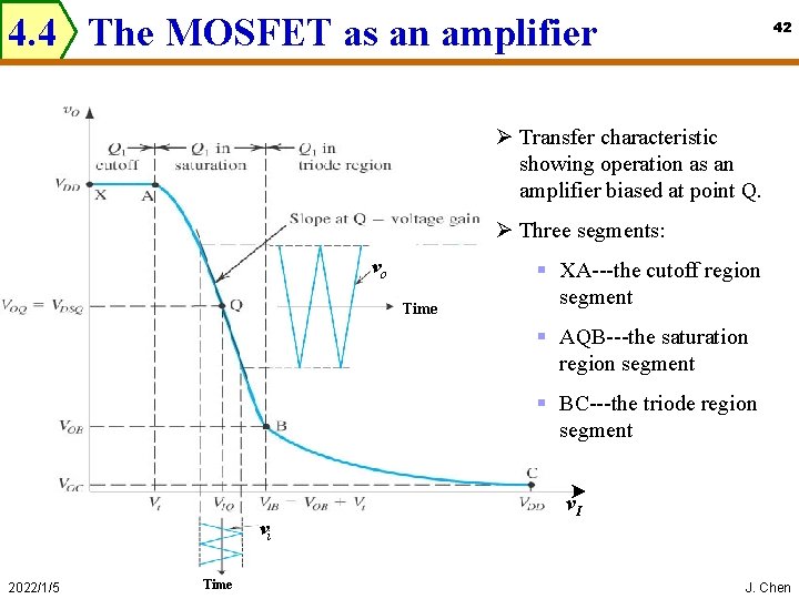
4. 4 The MOSFET as an amplifier 42 Ø Transfer characteristic showing operation as an amplifier biased at point Q. Ø Three segments: vo Time § XA---the cutoff region segment § AQB---the saturation region segment § BC---the triode region segment vi 2022/1/5 Time v. I J. Chen

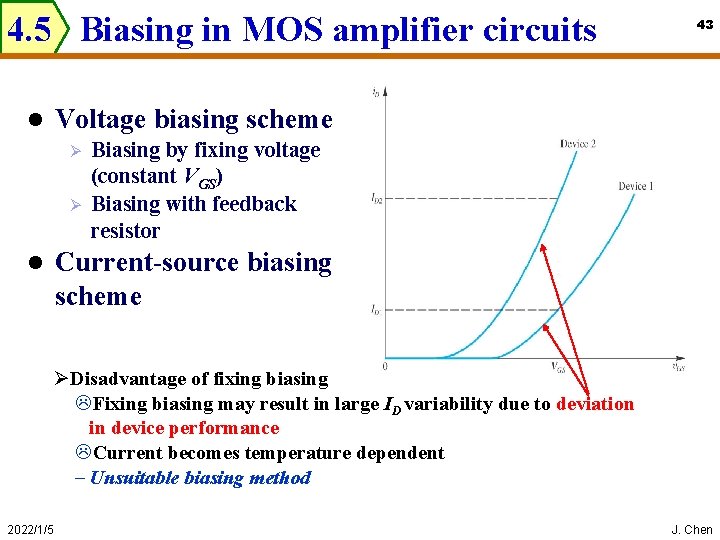
4. 5 Biasing in MOS amplifier circuits l Voltage biasing scheme Ø Ø l 43 Biasing by fixing voltage (constant VGS) Biasing with feedback resistor Current-source biasing scheme ØDisadvantage of fixing biasing LFixing biasing may result in large ID variability due to deviation in device performance LCurrent becomes temperature dependent - Unsuitable biasing method 2022/1/5 J. Chen

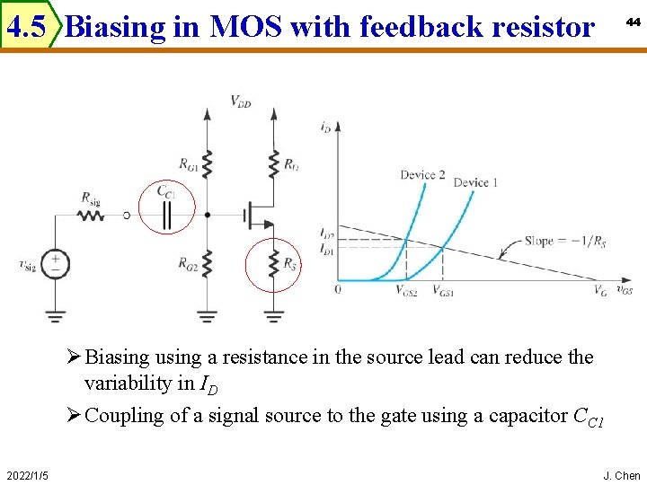
4. 5 Biasing in MOS with feedback resistor 44 Ø Biasing using a resistance in the source lead can reduce the variability in ID Ø Coupling of a signal source to the gate using a capacitor CC 1 2022/1/5 J. Chen

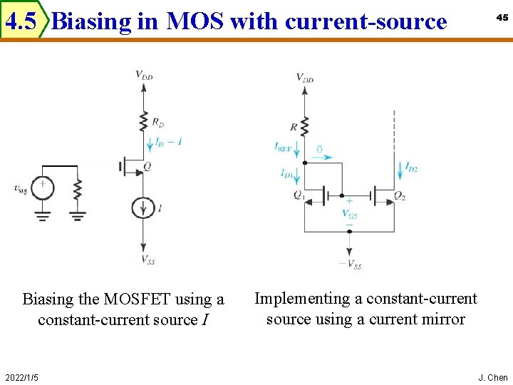
4. 5 Biasing in MOS with current-source Biasing the MOSFET using a constant-current source I 2022/1/5 45 Implementing a constant-current source using a current mirror J. Chen

4. 6 Small-signal operation and models l The ac characteristic Ø Definition of transconductance Ø Definition of output resistance Ø Definition of voltage gain l Small-signal 2022/1/5 46 model Ø Hybrid π model Ø T model Ø Modeling the body effect J. Chen

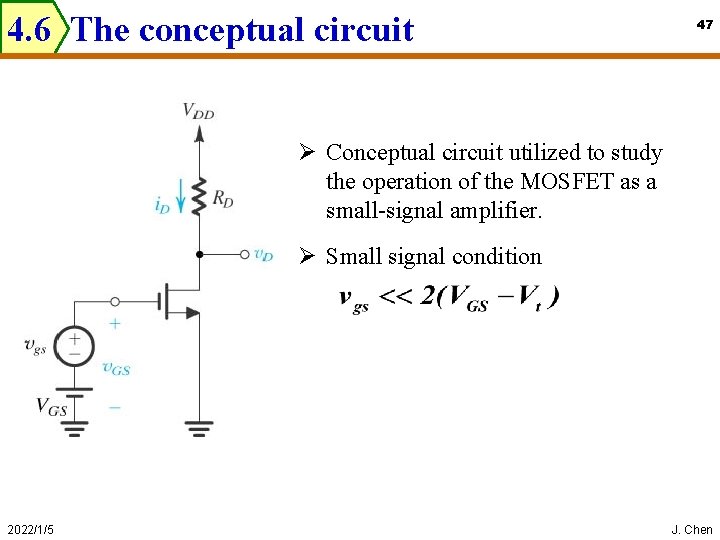
4. 6 The conceptual circuit 47 Ø Conceptual circuit utilized to study the operation of the MOSFET as a small-signal amplifier. Ø Small signal condition 2022/1/5 J. Chen

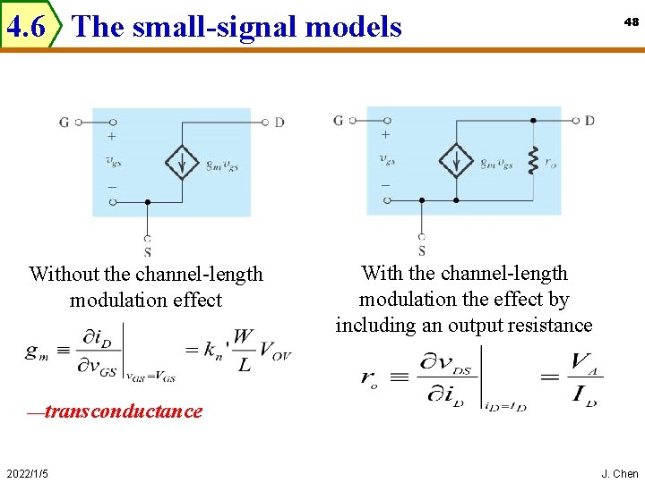
4. 6 The small-signal models Without the channel-length modulation effect 48 With the channel-length modulation the effect by including an output resistance —transconductance 2022/1/5 J. Chen

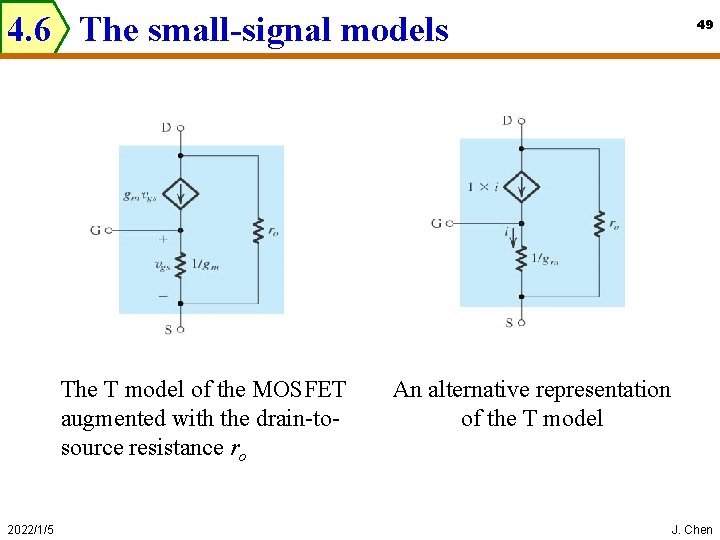
4. 6 The small-signal models The T model of the MOSFET augmented with the drain-tosource resistance ro 2022/1/5 49 An alternative representation of the T model J. Chen

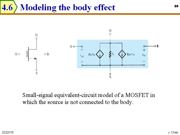
4. 6 Modeling the body effect 50 Small-signal equivalent-circuit model of a MOSFET in which the source is not connected to the body. 2022/1/5 J. Chen

4. 7 Single-stage MOS amplifier 2022/1/5 l Characteristic parameters l Three configurations Ø Common-source configuration Ø Common-drain configuration Ø Common-gate configuration 51 J. Chen

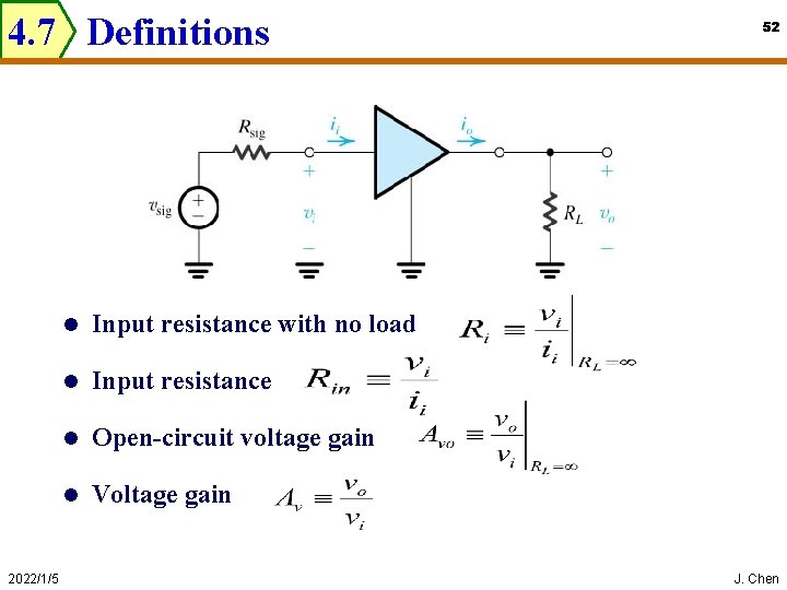
4. 7 Definitions 2022/1/5 l Input resistance with no load l Input resistance l Open-circuit voltage gain l Voltage gain 52 J. Chen

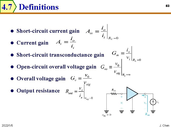
4. 7 Definitions l Short-circuit current gain l Current gain l Short-circuit transconductance gain l Open-circuit overall voltage gain l Output resistance 2022/1/5 53 J. Chen

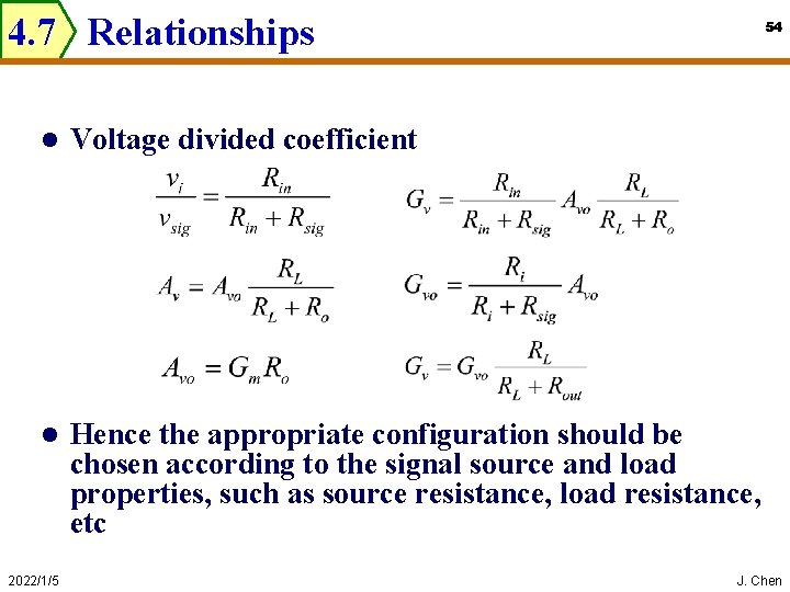
4. 7 Relationships 54 l Voltage divided coefficient l Hence the appropriate configuration should be chosen according to the signal source and load properties, such as source resistance, load resistance, etc 2022/1/5 J. Chen

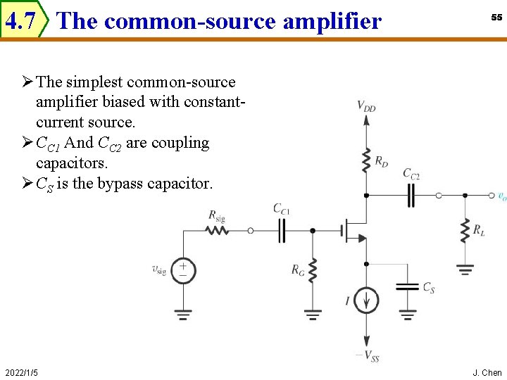
4. 7 The common-source amplifier 55 Ø The simplest common-source amplifier biased with constantcurrent source. Ø CC 1 And CC 2 are coupling capacitors. Ø CS is the bypass capacitor. 2022/1/5 J. Chen

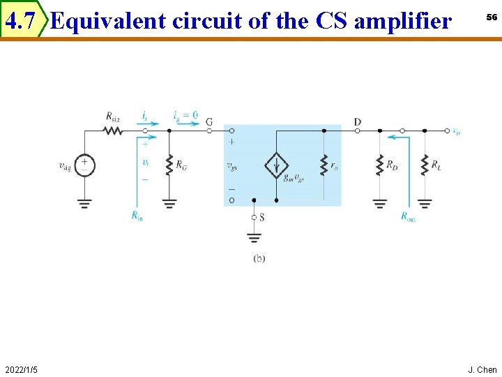
4. 7 Equivalent circuit of the CS amplifier 2022/1/5 56 J. Chen

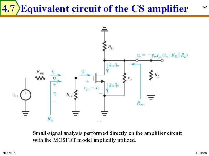
4. 7 Equivalent circuit of the CS amplifier 57 Small-signal analysis performed directly on the amplifier circuit with the MOSFET model implicitly utilized. 2022/1/5 J. Chen

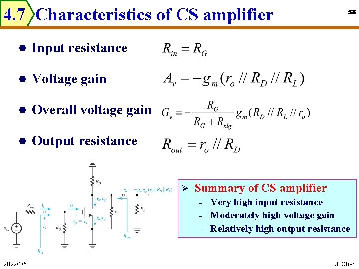
4. 7 Characteristics of CS amplifier l Input resistance l Voltage gain l Overall voltage gain l Output resistance Ø Summary of CS amplifier - 2022/1/5 58 Very high input resistance Moderately high voltage gain Relatively high output resistance J. Chen

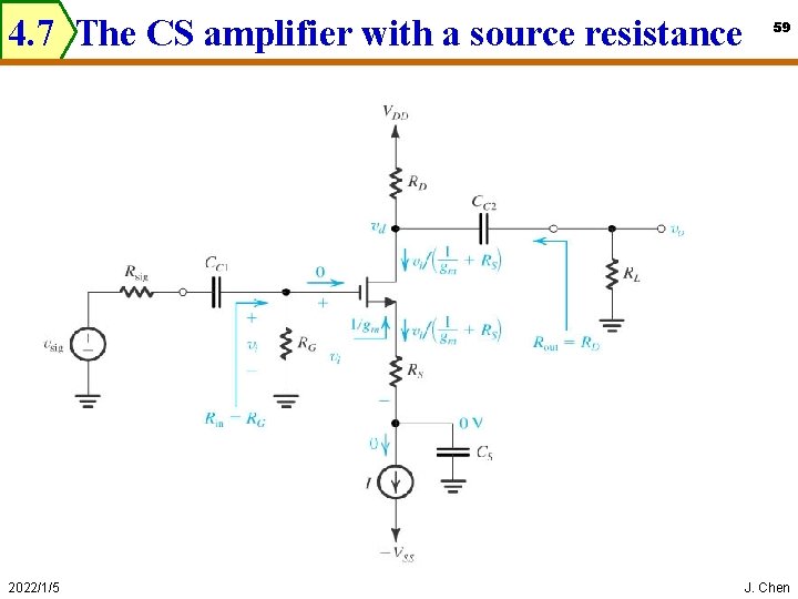
4. 7 The CS amplifier with a source resistance 2022/1/5 59 J. Chen

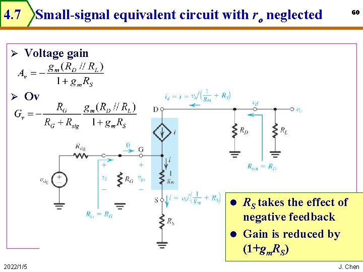
4. 7 Small-signal equivalent circuit with ro neglected Ø Voltage gain Ø Overall voltage gain 60 RS takes the effect of negative feedback l Gain is reduced by (1+gm. RS) l 2022/1/5 J. Chen

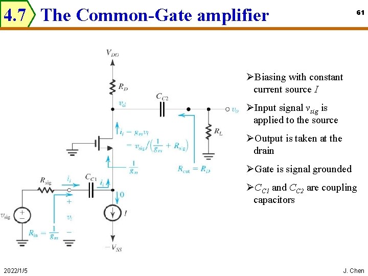
4. 7 The Common-Gate amplifier 61 ØBiasing with constant current source I ØInput signal vsig is applied to the source ØOutput is taken at the drain ØGate is signal grounded ØCC 1 and CC 2 are coupling capacitors 2022/1/5 J. Chen

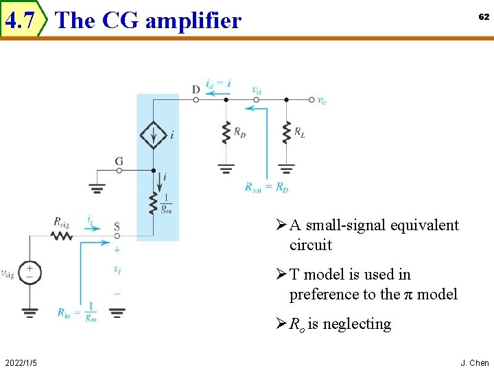
4. 7 The CG amplifier 62 Ø A small-signal equivalent circuit Ø T model is used in preference to the π model Ø Ro is neglecting 2022/1/5 J. Chen

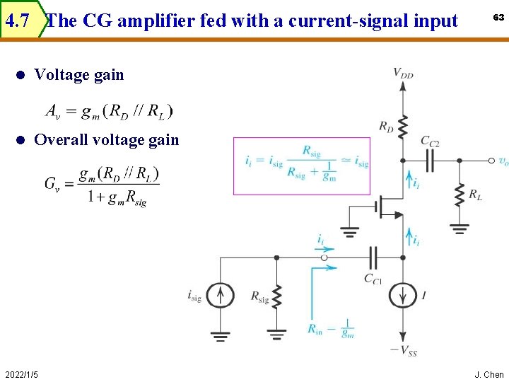
4. 7 The CG amplifier fed with a current-signal input l Voltage gain l Overall voltage gain 2022/1/5 63 J. Chen

4. 7 Summary of CG amplifier 64 l Noninverting amplifier l Low input resistance l Relatively high output resistance l Current follower l Superior high-frequency performance 2022/1/5 J. Chen

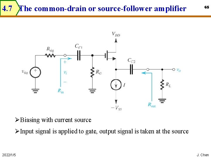
4. 7 The common-drain or source-follower amplifier 65 ØBiasing with current source ØInput signal is applied to gate, output signal is taken at the source 2022/1/5 J. Chen

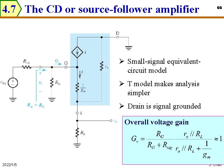
4. 7 The CD or source-follower amplifier 66 Ø Small-signal equivalentcircuit model Ø T model makes analysis simpler Ø Drain is signal grounded Overall voltage gain 2022/1/5 J. Chen

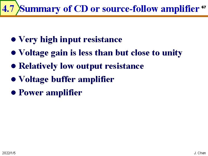
4. 7 Summary of CD or source-follow amplifier 67 l Very high input resistance l Voltage gain is less than but close to unity l Relatively low output resistance l Voltage buffer amplifier l Power amplifier 2022/1/5 J. Chen

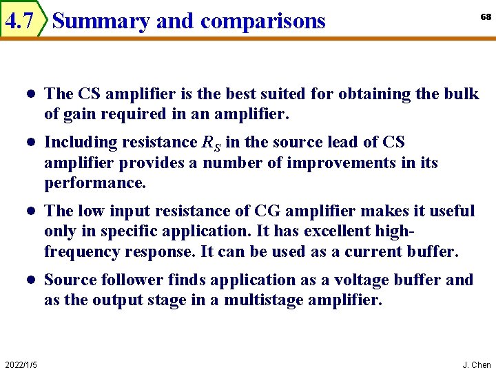
4. 7 Summary and comparisons 68 l The CS amplifier is the best suited for obtaining the bulk of gain required in an amplifier. l Including resistance RS in the source lead of CS amplifier provides a number of improvements in its performance. l The low input resistance of CG amplifier makes it useful only in specific application. It has excellent highfrequency response. It can be used as a current buffer. l Source follower finds application as a voltage buffer and as the output stage in a multistage amplifier. 2022/1/5 J. Chen

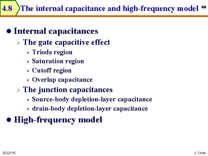
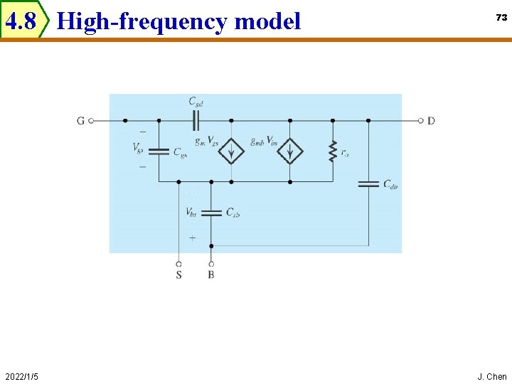
4. 8 The internal capacitance and high-frequency model l Internal Ø capacitances The gate capacitive effect § § Ø Triode region Saturation region Cutoff region Overlap capacitance The junction capacitances § § Source-body depletion-layer capacitance drain-body depletion-layer capacitance l High-frequency 2022/1/5 69 model J. Chen

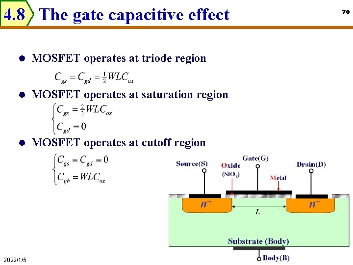
4. 8 The gate capacitive effect l MOSFET operates at triode region l MOSFET operates at saturation region l MOSFET operates at cutoff region 2022/1/5 70 J. Chen

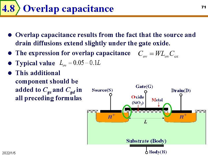
4. 8 Overlap capacitance 71 Overlap capacitance results from the fact that the source and drain diffusions extend slightly under the gate oxide. l The expression for overlap capacitance l Typical value l This additional component should be added to Cgs and Cgd in all preceding formulas l 2022/1/5 J. Chen

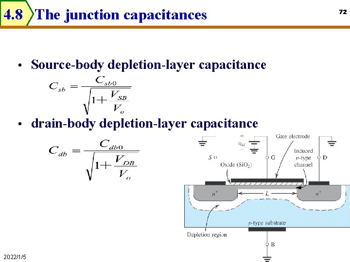
4. 8 The junction capacitances • Source-body depletion-layer capacitance • drain-body depletion-layer capacitance 2022/1/5 72 J. Chen

4. 8 High-frequency model 2022/1/5 73 J. Chen

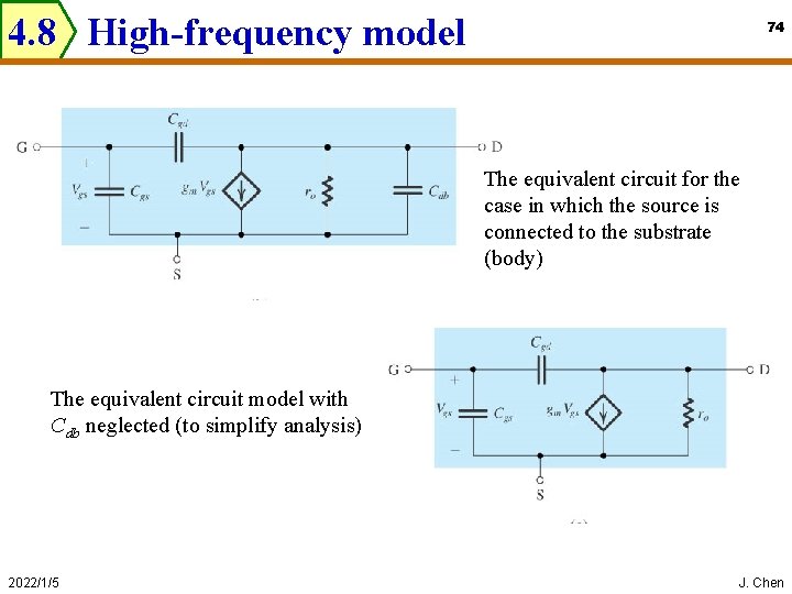
4. 8 High-frequency model 74 The equivalent circuit for the case in which the source is connected to the substrate (body) The equivalent circuit model with Cdb neglected (to simplify analysis) 2022/1/5 J. Chen

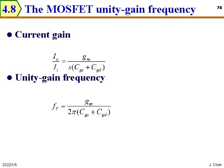
4. 8 The MOSFET unity-gain frequency l Current gain l Unity-gain 2022/1/5 75 frequency J. Chen

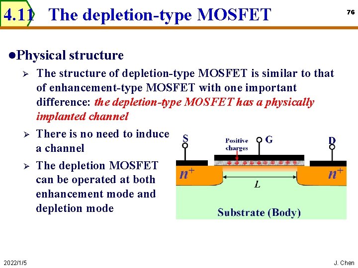
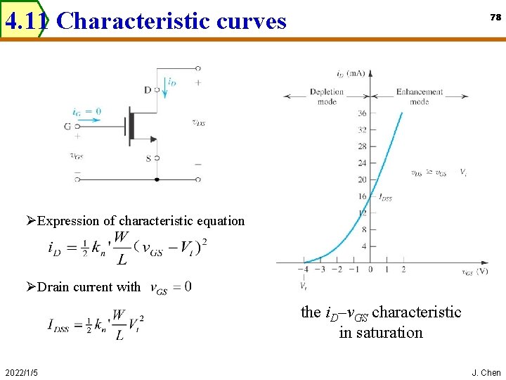
4. 11 The depletion-type MOSFET l. Physical Ø Ø Ø 2022/1/5 76 structure The structure of depletion-type MOSFET is similar to that of enhancement-type MOSFET with one important difference: the depletion-type MOSFET has a physically implanted channel There is no need to induce a channel The depletion MOSFET can be operated at both enhancement mode and depletion mode J. Chen

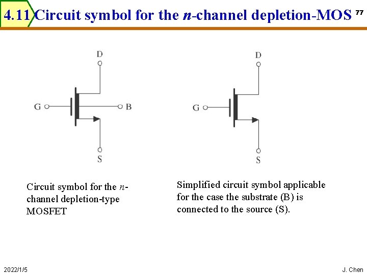
4. 11 Circuit symbol for the n-channel depletion-MOS Circuit symbol for the nchannel depletion-type MOSFET 2022/1/5 77 Simplified circuit symbol applicable for the case the substrate (B) is connected to the source (S). J. Chen

4. 11 Characteristic curves 78 ØExpression of characteristic equation ØDrain current with the i. D–v. GS characteristic in saturation 2022/1/5 J. Chen

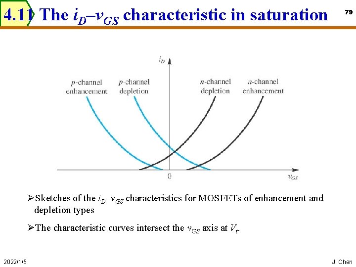
4. 11 The i. D–v. GS characteristic in saturation 79 ØSketches of the i. D–v. GS characteristics for MOSFETs of enhancement and depletion types ØThe characteristic curves intersect the v. GS axis at Vt. 2022/1/5 J. Chen

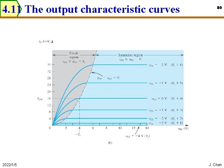
4. 11 The output characteristic curves 2022/1/5 80 J. Chen

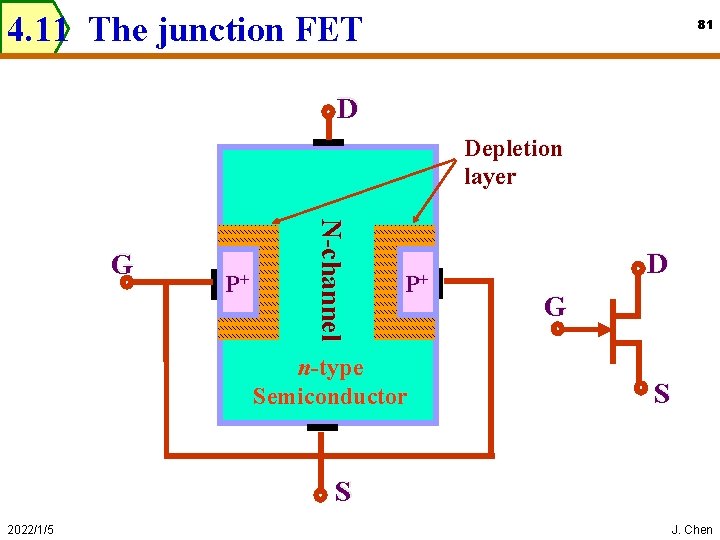
4. 11 The junction FET 81 D Depletion layer P+ N-channel G P+ n-type Semiconductor D G S S 2022/1/5 J. Chen

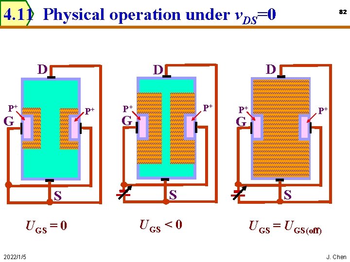
4. 11 Physical operation under v. DS=0 D P+ G S UGS = 0 2022/1/5 D D P+ 82 P+ P+ G S UGS < 0 S UGS = UGS(off) J. Chen

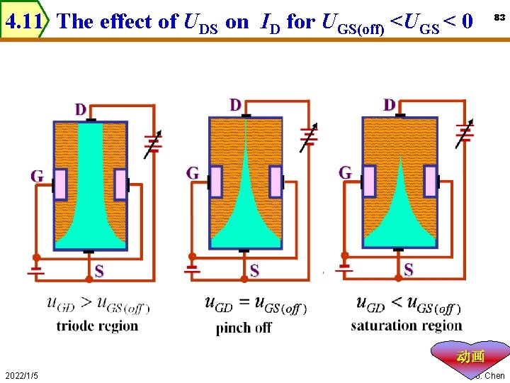
4. 11 The effect of UDS on ID for UGS(off) <UGS < 0 83 动画 2022/1/5 J. Chen

Homework 84 l March 18, 2013: D 4. 14; 4. 15; 4. 19;D 4. 21; l March 25, 2013: D 4. 36;D 4. 37; 4.68; 4.75; 4. 79; l April 1, 2013: 4. 85; 4. 91; 4. 92; 4. 94; 4. 96; 4. 102 2022/1/5 J. Chen