MOS FieldEffect Transistors MOSFETs Introduction The voltage between
")
MOS Field-Effect Transistors (MOSFETs)

Introduction • The voltage between two terminals controls the current flow in the third terminal — Field Effect • Can be used as an amp and as a switch • Current is conducted by only one type of carrier (electron or hole) — unipolar transistor • Basic concept: 1930 s • Practical reality : 1960 s • Metal-oxide semiconductor FET (MOSFET) 출현 및 각광받음

Introduction • Comparison to BJT - Occupying small silicon area - Manufacturing process is relatively simple - Digital logic and memory can be implemented with only MOSFET circuits (no resistor or diodes are needed. ) - VLSI (very large scale integrated circuit) possible (예, u-p) - MOS tech. Has been applied in the design of analog circuit and integrated circuit that combine both analog and digital circuits. • 가장 중요하게 사용되는 기술인 Enhanced – type MOSFET에 대해서 주로 다루게 될 것임.

5. 1 Device structure and physical operation • Device Structure Figure 5. 1 Physical structure of the enhancement-type NMOS transistor: (a) perspective view; (b) cross-section. Typically L = 0. 1 to 3 mm, W = 0. 2 to 100 mm, and the thickness of the oxide layer (tox) is in the range of 2 to 50 nm.

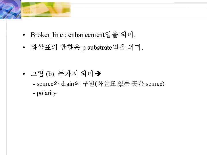
• Fabricated on a p-type substrate : single crystal silicon wafer that provides physical support. • Source and drain : heavily doped regions • Si. O 2 (Silicon dioxide): insulator, covering the area between the source and drain regions. • Metal is deposited on top of the oxide layer (Gate) • Metal contacts (Drain, Source, Substrate) Four terminals (Gate, Source, Drain, Substrate)
")
• 일반 FET들은 gate에 metal 사용 않음, 요즘 MOSFET들은 silicon gate technology (Polysilicon) 사용 • MOSFET의 다름 이름: insulate-gate FET=IGFET - The name arises from the physical structure of the device. • Substrate forms pn junction with the source and drain. • In normal operation, pn junctions are kept reverse-biased. • Substrate가 source에 연결되면 substrate는 아무런 역할을 하지 않은 것 처럼 보임. treated as a three-terminal device

• Gate voltage controls the current flow between source and drain • Channel region: L, W very important parameter - L: 1 -10 um, W: 2 -500 um - 1 um이하의 L은 high-speed digital integrated-circuit 에 사용 • BJT와는 달리, symmetrical device로 만들어짐 source and drain can be interchanged.

• Operation with No Gate Voltage - Two back-to-back diodes exist in series between drain and source. Prevent current conduction from drain to source when a voltage is applied. The path between drain to source has a very high resistance.

• Creating a Channel for Current Flow • Source, Drain grounded • Gate positive voltage Figure 5. 2 The enhancement-type NMOS transistor with a positive voltage applied to the gate. An n channel is induced at the top of the substrate beneath the gate.

• Positive gate voltage free holes are repelled from the region of the substrate under the gate carrier-depletion region 이 영역에 bound negative charge를 생성시킴 • 또한, N+인 drain 및 source영역으로부터 Channel region으로 전자를 유인함 n region is created and connect the source and drain regions with small , current flows through the induced n region === n-channel MOSFET (NMOS).

• Threshold voltage : The voltage to form a conducting channel Typical =[1, 3]V • Capacitor dielectric : Gate의 금속판에 +가 대전되게 하고 channel에 – 전하가 축적되어 생성.

• Applying a Small Figure 5. 3 An NMOS transistor with v. GS > Vt and with a small v. DS applied. The device acts as a resistance whose value is determined by v. GS. Specifically, the channel conductance is proportional to v. GS – Vt’ and thus i. D is proportional to (v. GS – Vt) v. DS. Note that the depletion region is not shown (for simplicity).
 : causes a current , magnitude")
• Small (0. 1 -0. 2 v) : causes a current , magnitude of is depends on the density of electrons in the channel, which in turn depends on the magnitude of. • If , the channel is just induced and the current is still negligibly small. The conductance of the channel is proportional to the excess gate voltage or effective voltage. ( ). 전류는 의 크기와 에 비례. • Enhancement-type MOSFET; The type to enhance the channel. - ,

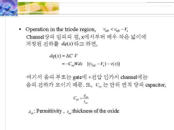
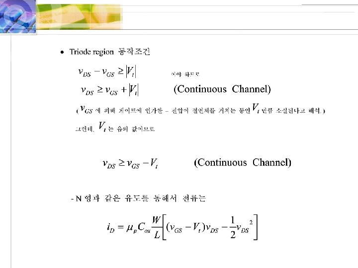
• Operation as is increased • is held constant at a value grater than • drops across the length of the channel • Voltage between gate and the arbitrary point is - : at the source : at the drain • Channel 의 폭(depth)은 이 전압 값에 비례하므로 이 폭은 전체 channel 에서 균일하지 않음; rather, the channel will take the tapered form. == Fig. 5. 7

Figure 5. 7 Increasing v. DS causes the channel to acquire a tapered shape. Eventually, as v. DS reaches v. GS – Vt’ the channel is pinched off at the drain end. Increasing v. DS above v. GS – Vt has little effect (theoretically, no effect) on the channel’s shape.
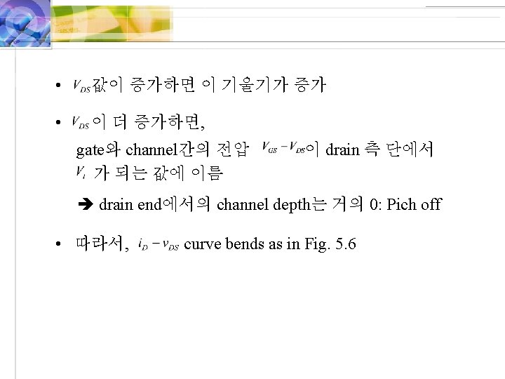

Figure 5. 6 The drain current i. D versus the drain-to-source voltage v. DS for an enhancement-type NMOS transistor operated with v. GS > Vt.

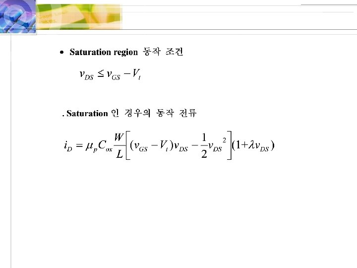
• 값은 pinch off보다 더 증가해도 이론적으로는 channel shape 불변, 전류 값 불변 Drain current Saturation • 따라서, • 의 saturation 전압 값에 따라서 saturation region, triode region

Derivation of the Figure 5. 8 Derivation of the i. D–v. DS characteristic of the NMOS transistor. relationship
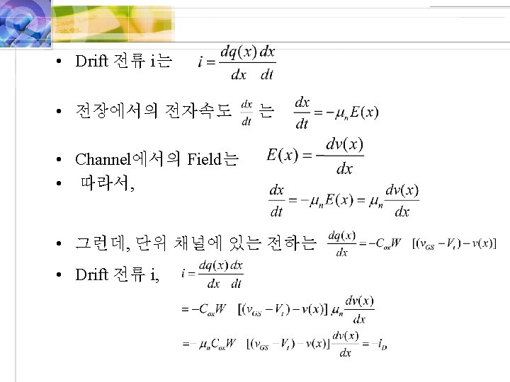

• Rearranging • Integrating • gives, Current at the triode region

• Saturation인 경우, 이므로 • Process transconductance parameter : : Observe that the drain current is proportional to the ratio of the channel width W to the channel length L (aspect ratio).

• P-channel MOSFET • 및 • <0 <0 • bigger, slower than NMOS • higher supply voltage • 주로 CMOS 기술에서 NMOS와 함께 사용.

• Complementary MOS or CMOS Figure 5. 9 Cross-section of a CMOS integrated circuit. Note that the PMOS transistor is formed in a separate n-type region, known as an n well. Another arrangement is also possible in which an n-type body is used and the n device is formed in a p well. Not shown are the connections made to the p-type body and to the n well; the latter functions as the body terminal for the p-channel device.

• More difficult to fabricate than NMOS • Most useful • Take over many applications with bipolar tr. • P 영역을 만들기 위해 p substrate에 n well 설치 • N mos와 P mos 간에는 뚜꺼운 Si. O 2를 사용하여 isolation

5. 2 Current-Voltage Characteristic of the Enhancement MOSFET • Circuit symbol Figure 5. 10 (a) Circuit symbol for the n-channel enhancement-type MOSFET. (b) Modified circuit symbol with an arrowhead on the source terminal to distinguish it from the drain and to indicate device polarity (i. e. , n channel). (c) Simplified circuit symbol to be used when the source is connected to the body or when the effect of the body on device operation is unimportant.
 An n-channel enhancement-type MOSFET with v.")
• The Characteristics Figure 5. 11 (a) An n-channel enhancement-type MOSFET with v. GS and v. DS applied and with the normal directions of current flow indicated. (b) The i. D–v. DS characteristics for a device with k’n (W/L) = 1. 0 m. A/V 2.

• Three distinctive regions: - curoff, triode, saturation regions - (BJT의 그림 5. 13와 비교) • Saturation region - used if the FET is operate as an amplifier • Cutoff and triode region - used for a switch Fig. 5. 13
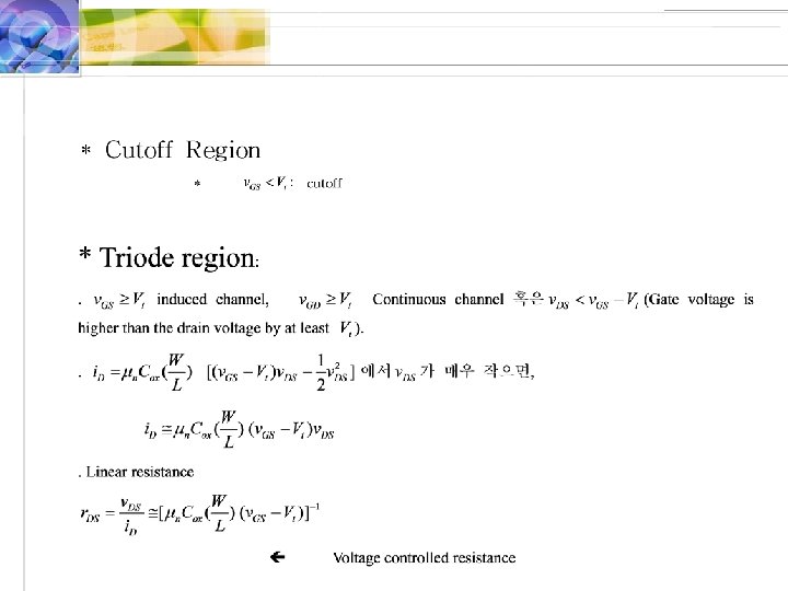

Figure 5. 12 The i. D–v. GS characteristic for an enhancement-type NMOS transistor in saturation (Vt = 1 V, k’n W/L = 1. 0 m. A/V 2).

Figure 5. 13 Large-signal equivalent-circuit model of an n-channel MOSFET operating in the saturation region.


Figure 5. 14 The relative levels of the terminal voltages of the enhancement NMOS transistor for operation in the triode region and in the saturation region.

• Finite Output Resistance in Saturation Figure 5. 15 Increasing v. DS beyond v. DSsat causes the channel pinch-off point to move slightly away from the drain, thus reducing the effective channel length (by DL).
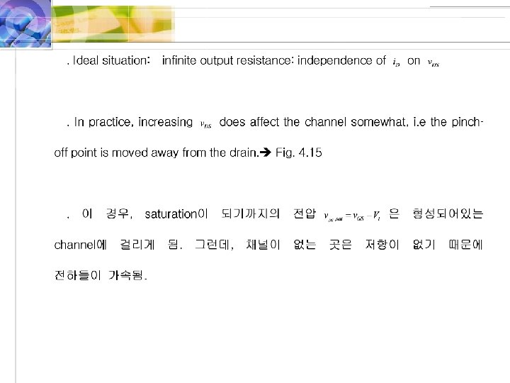

Figure 5. 16 Effect of v. DS on i. D in the saturation region. The MOSFET parameter VA depends on the process technology and, for a given process, is proportional to the channel length L.


Figure 5. 17 Large-signal equivalent circuit model of the n-channel MOSFET in saturation, incorporating the output resistance ro. The output resistance models the linear dependence of i. D on v. DS and is given by Eq. (5. 22).

• Characteristics of the p-channel MOSFET
 Circuit symbol for the p-channel enhancement-type MOSFET. (b) Modified symbol")
Figure 5. 18 (a) Circuit symbol for the p-channel enhancement-type MOSFET. (b) Modified symbol with an arrowhead on the source lead. (c) Simplified circuit symbol for the case where the source is connected to the body. (d) The MOSFET with voltages applied and the directions of current flow indicated. Note that v. GS and v. DS are negative and i. D flows out of the drain terminal.

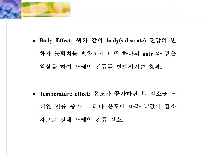
• Role of the Substrate-The body effect
- Slides: 48