Institut fr Theoretische Elektrotechnik Large Signal Modeling of


- Slides: 25
Institut für Theoretische Elektrotechnik Large Signal Modeling of Inversion-Mode MOS Varactors in VCOs MOS-AK Meeting 2009 2 -3 April 2009 at IHP in Frankfurt (Oder) Dipl. -Ing. Jan Bremer
Institut für Theoretische Elektrotechnik Overview § § § Motivation Large Signal Modeling of Varactors in VCOs Alternative Modeling Concept Simulation Results Conclusion Jan Bremer Large Signal Capacitance Modeling 03. 04. 2009 page 2
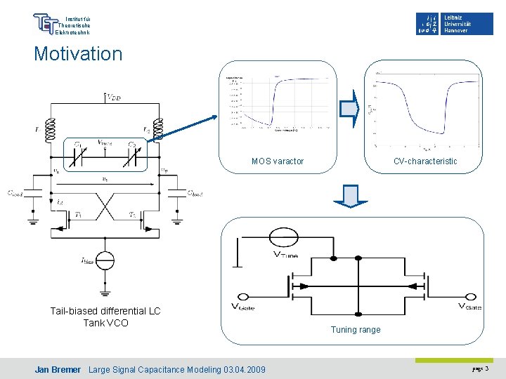
Institut für Theoretische Elektrotechnik Motivation MOS varactor Tail-biased differential LC Tank VCO Jan Bremer Large Signal Capacitance Modeling 03. 04. 2009 CV-characteristic Tuning range page 3
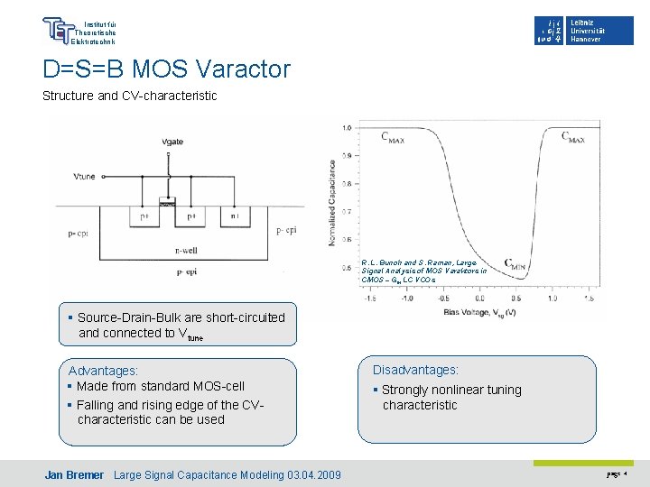
Institut für Theoretische Elektrotechnik D=S=B MOS Varactor Structure and CV-characteristic R. L. Bunch and S. Raman, Large. Signal Analysis of MOS Varaktors in CMOS – Gm LC VCOs § Source-Drain-Bulk are short-circuited and connected to Vtune Advantages: § Made from standard MOS-cell § Falling and rising edge of the CVcharacteristic can be used Jan Bremer Large Signal Capacitance Modeling 03. 04. 2009 Disadvantages: § Strongly nonlinear tuning characteristic page 4
Institut für Theoretische Elektrotechnik Accumulation Mode MOS Varactor Structure and CV-characteristic R. L. Bunch and S. Raman, Large. Signal Analysis of MOS Varaktors in CMOS – Gm LC VCOs § the p+ regions of drain and source are replaced with n+ regions Advantages: § Wider transition from Cmin to Cmax as inversion mode varactors § Best Cmax / Cmin ratio § Lowest parasitic resistance Jan Bremer Large Signal Capacitance Modeling 03. 04. 2009 Disadvantages: § Not made from standard MOS-cell § Nonlinear tuning characteristic page 5
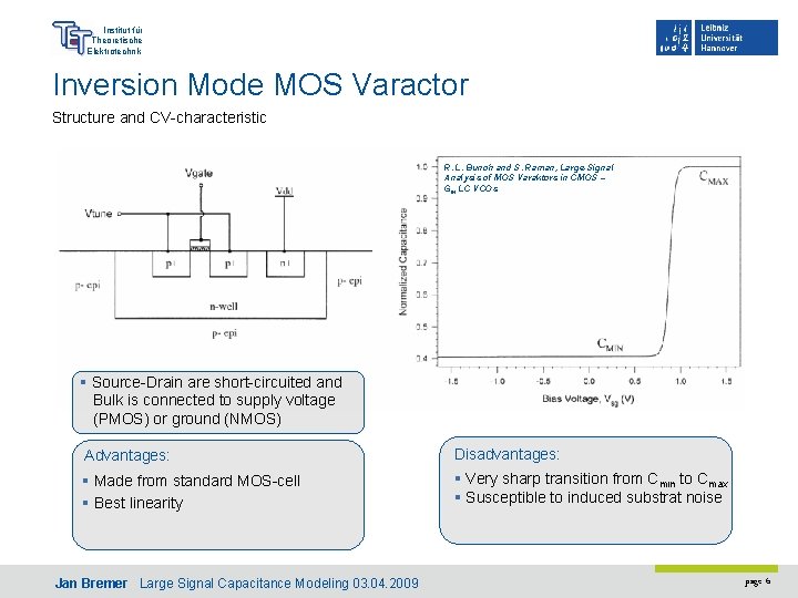
Institut für Theoretische Elektrotechnik Inversion Mode MOS Varactor Structure and CV-characteristic R. L. Bunch and S. Raman, Large-Signal Analysis of MOS Varaktors in CMOS – Gm LC VCOs § Source-Drain are short-circuited and Bulk is connected to supply voltage (PMOS) or ground (NMOS) Advantages: Disadvantages: § Made from standard MOS-cell § Best linearity § Very sharp transition from Cmin to Cmax § Susceptible to induced substrat noise Jan Bremer Large Signal Capacitance Modeling 03. 04. 2009 page 6
Institut für Theoretische Elektrotechnik Overview § § § Motivation Large Signal Modeling of Varactors in VCOs Alternative Modeling Concept Simulation Results Conclusion Jan Bremer Large Signal Capacitance Modeling 03. 04. 2009 page 7
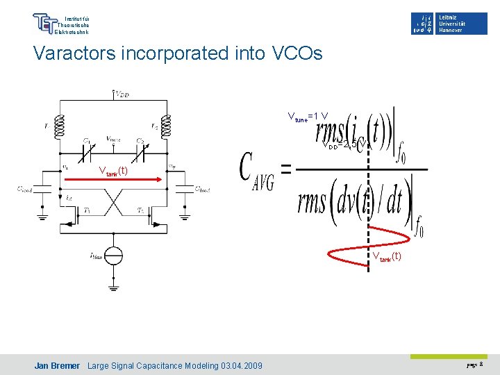
Institut für Theoretische Elektrotechnik Varactors incorporated into VCOs Vtune=1 V VDD=2, 5 V Vtank(t) Jan Bremer Large Signal Capacitance Modeling 03. 04. 2009 page 8
Institut für Theoretische Elektrotechnik Large Signal Varactor Modeling after R. L. Bunch Small-Signal A=1. 0 V Capacitance A=0. 1 V A=0. 5 V Gate voltage § Expression for C(v(t)) is needed § Averaging is subject for debate § Neglecting the higher harmonics § Amplitude of the output signal of the VCO is needed R. L. Bunch and S. Raman, Large-Signal Analysis of MOS Varaktors in CMOS – G m LC VCOs Jan Bremer Large Signal Capacitance Modeling 03. 04. 2009 page 9
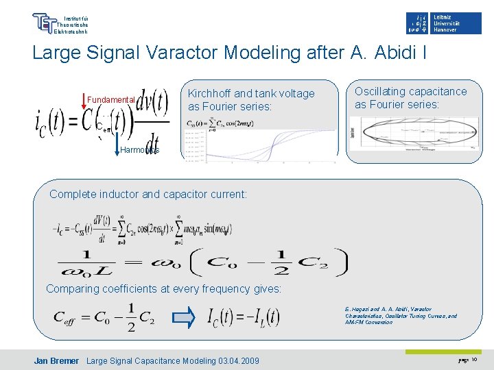
Institut für Theoretische Elektrotechnik Large Signal Varactor Modeling after A. Abidi I Fundamental Kirchhoff and tank voltage as Fourier series: Oscillating capacitance as Fourier series: Ceff Harmonics Complete inductor and capacitor current: Comparing coefficients at every frequency gives: E. Hegazi and A. A. Abidi, Varactor Characteristics, Oscillator Tuning Curves, and AM-FM Conversion Jan Bremer Large Signal Capacitance Modeling 03. 04. 2009 page 10
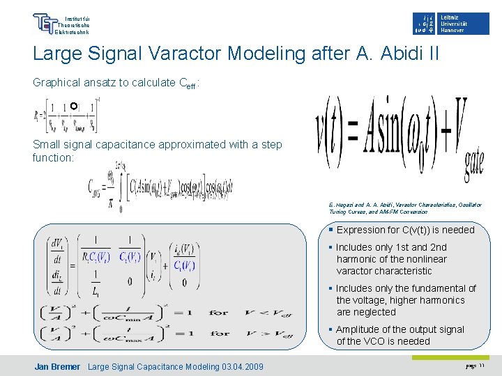
Institut für Theoretische Elektrotechnik Large Signal Varactor Modeling after A. Abidi II Graphical ansatz to calculate Ceff : Small signal capacitance approximated with a step function: E. Hegazi and A. A. Abidi, Varactor Characteristics, Oscillator Tuning Curves, and AM-FM Conversion § Expression for C(v(t)) is needed § Includes only 1 st and 2 nd harmonic of the nonlinear varactor characteristic § Includes only the fundamental of the voltage, higher harmonics are neglected § Amplitude of the output signal of the VCO is needed Jan Bremer Large Signal Capacitance Modeling 03. 04. 2009 page 11
Institut für Theoretische Elektrotechnik Overview § § § Motivation Large Signal Modeling of Varactors in VCOs Alternative Modeling Concept Simulation Results Conclusion Jan Bremer Large Signal Capacitance Modeling 03. 04. 2009 page 12
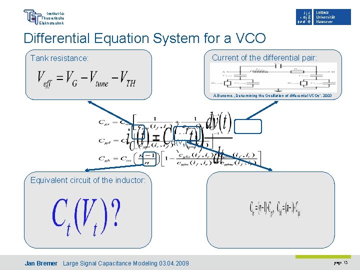
Institut für Theoretische Elektrotechnik Differential Equation System for a VCO Current of the differential pair: Tank resistance: A. Bunomo, „Determining the Oscillation of differential VCOs“, 2003 C(Vt) Equivalent circuit of the inductor: Jan Bremer Large Signal Capacitance Modeling 03. 04. 2009 page 13
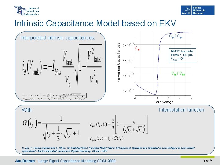
Institut für Theoretische Elektrotechnik Intrinsic Capacitance Model based on EKV Cgs / Cgd Normalized Capacitances Interpolated intrinsic capacitances: Cgb NMOS transistor Width = 100 µm Vtune = 0 V Cbs / Cbd Gate Voltage With: Interpolation function: C. Enz, F. Krummenacher and E. Vittoz, ”An Analytical MOS Transistor Model Valid in All Regions of Operation and Dedicated to Low-Voltage and Low-Current Applications”, Analog Integrated Circuits and Signal Processing, Kluwer, 1995 Jan Bremer Large Signal Capacitance Modeling 03. 04. 2009 page 14
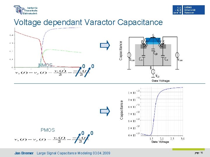
Institut für Theoretische Elektrotechnik Capacitance Voltage dependant Varactor Capacitance NMOS 0 0 Capacitance Gate Voltage PMOS 0 0 Gate Voltage Jan Bremer Large Signal Capacitance Modeling 03. 04. 2009 page 15
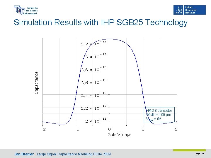
Institut für Theoretische Elektrotechnik Capacitance Simulation Results with IHP SGB 25 Technology NMOS transistor Width = 100 µm Vtune = 0 V Gate Voltage Jan Bremer Large Signal Capacitance Modeling 03. 04. 2009 page 16
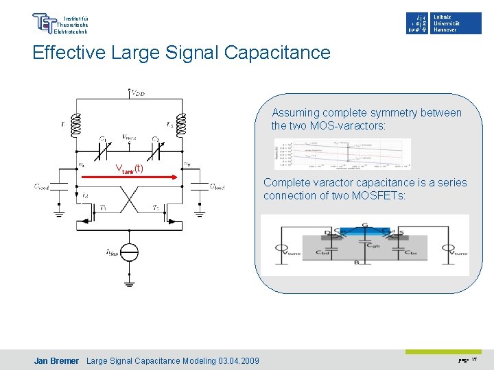
Institut für Theoretische Elektrotechnik Effective Large Signal Capacitance Assuming complete symmetry between the two MOS-varactors: Vtank(t) Complete varactor capacitance is a series connection of two MOSFETs: Jan Bremer Large Signal Capacitance Modeling 03. 04. 2009 page 17
Institut für Theoretische Elektrotechnik Overview § § § Motivation Large Signal Modeling of Varactors in VCOs Alternative Modeling Concept Simulation Results Conclusion Jan Bremer Large Signal Capacitance Modeling 03. 04. 2009 page 18
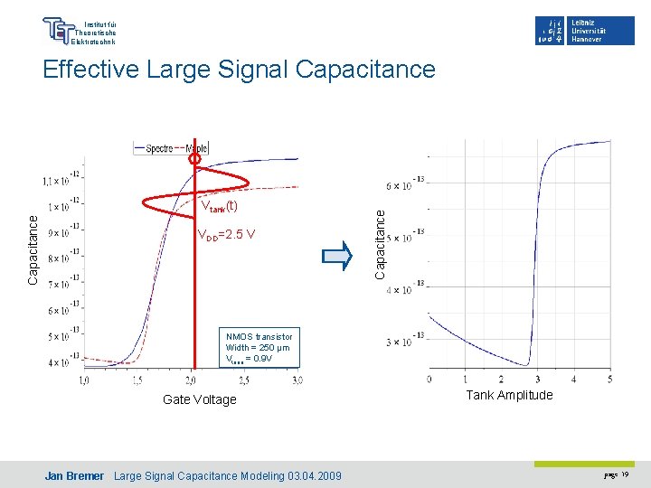
Institut für Theoretische Elektrotechnik Capacitance Vtank(t) VDD=2. 5 V Capacitance Effective Large Signal Capacitance NMOS transistor Width = 250 µm Vtune = 0. 9 V Gate Voltage Jan Bremer Large Signal Capacitance Modeling 03. 04. 2009 Tank Amplitude page 19
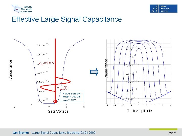
Institut für Theoretische Elektrotechnik Capacitance Effective Large Signal Capacitance VDD=2. 5 V Vtank(t) NMOS transistor Width = 250 µm Vtune = 1. 5 V Gate Voltage Jan Bremer Large Signal Capacitance Modeling 03. 04. 2009 Tank Amplitude page 20
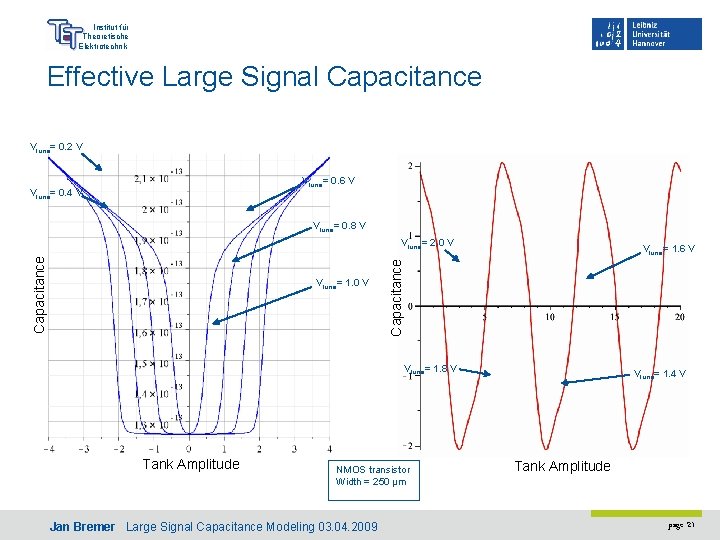
Institut für Theoretische Elektrotechnik Effective Large Signal Capacitance Vtune= 0. 2 V Vtune= 0. 6 V Vtune= 0. 4 V Vtune= 0. 8 V Vtune= 1. 0 V Vtune= 1. 6 V Capacitance Vtune= 2. 0 V Vtune= 1. 8 V Tank Amplitude NMOS transistor Width = 250 µm Jan Bremer Large Signal Capacitance Modeling 03. 04. 2009 Vtune= 1. 4 V Tank Amplitude page 21
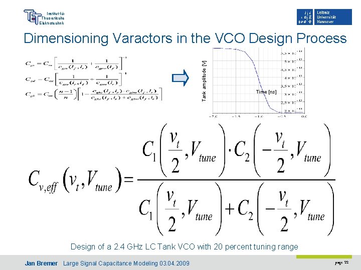
Institut für Theoretische Elektrotechnik Tank amplitude [V] Dimensioning Varactors in the VCO Design Process Time [ns] Design of a 2. 4 GHz LC Tank VCO with 20 percent tuning range Jan Bremer Large Signal Capacitance Modeling 03. 04. 2009 page 22
Institut für Theoretische Elektrotechnik Overview § § § Motivation Large Signal Modeling of Varactors in VCOs Alternative Modeling Concept Simulation Results Conclusion Jan Bremer Large Signal Capacitance Modeling 03. 04. 2009 page 23
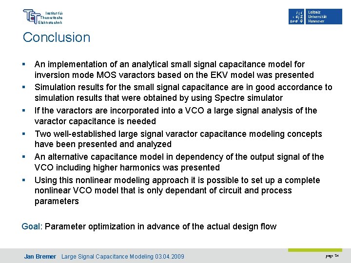
Institut für Theoretische Elektrotechnik Conclusion § § § An implementation of an analytical small signal capacitance model for inversion mode MOS varactors based on the EKV model was presented Simulation results for the small signal capacitance are in good accordance to simulation results that were obtained by using Spectre simulator If the varactors are incorporated into a VCO a large signal analysis of the varactor capacitance is needed Two well-established large signal varactor capacitance modeling concepts have been presented analyzed An alternative capacitance model in dependency of the output signal of the VCO including higher harmonics was presented Using this nonlinear modeling approach it is possible to set up a complete nonlinear VCO model that is only dependant of circuit and process parameters Goal: Parameter optimization in advance of the actual design flow Jan Bremer Large Signal Capacitance Modeling 03. 04. 2009 page 24
Institut für Theoretische Elektrotechnik The End Thank you for your attention! Jan Bremer Large Signal Capacitance Modeling 03. 04. 2009 page 25