The Microcontroller Architecture 1 Introduction to 8051 Microcontroller



- Slides: 47

The Microcontroller Architecture 1

Introduction to 8051 Microcontroller • Introduced by Intel in 1981 • An 8 bit microcontroller • It has 128 bytes of RAM, 4 K bytes of on – chip ROM, two timers, one serial port and four I/O ports all on a single chip • Intel refers to microcontroller 8051 as MCS-51. 2

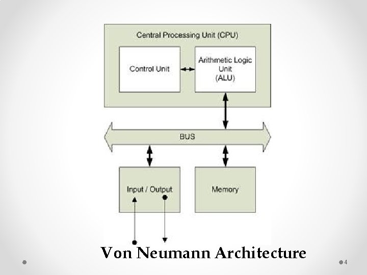
Von Neumann Architecture • In this architecture computers have a single, common memory space in which both program instructions and data are stored. • There is a single internal data bus that fetches both instructions and data. • They can not be performed at the same time 3

Von Neumann Architecture 4

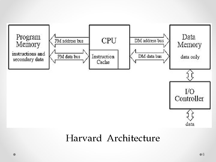
Harvard Architecture • Harvard architecture: computers have separate memory areas for program instructions and data. • There are two or more internal data buses, which allow simultaneous access to both instructions and data. • The CPU fetches program instructions on the program memory bus. 5

Harvard Architecture 6

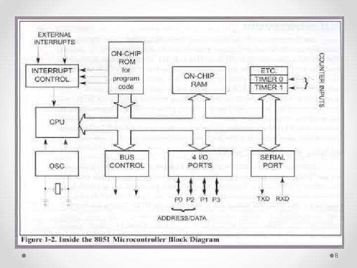
• Features of the 8051 core are : o o o o o 8 bit CPU 64 KB program memory address space 64 – KB data memory address space 4 – KB of on- chip program memory 128 bytes of on – chip data random access memory 32 bidirectional and individually addressable I/O lines Two 16 – bit timers/counters On chip clock oscillator Interrupt control 7

8

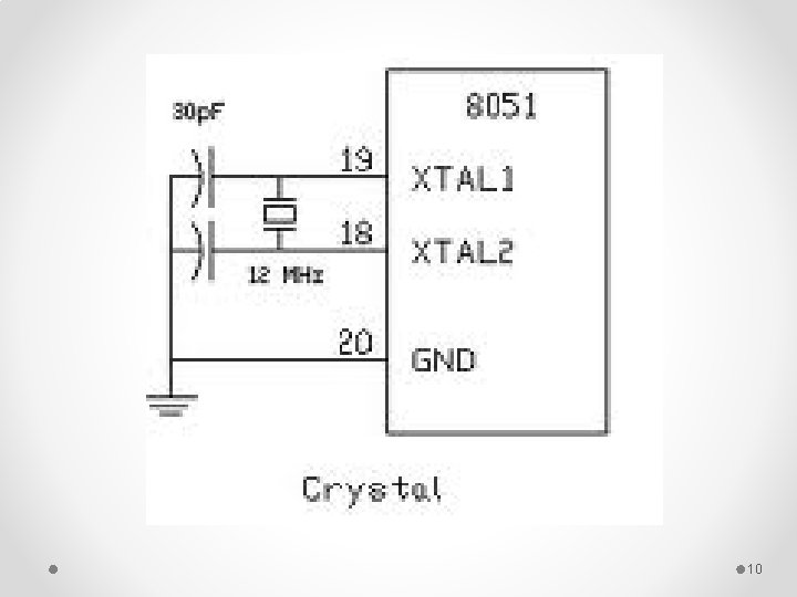
Oscillator • Pulses generated by the oscillator enable harmonic and synchronous operation of all circuits within the microcontroller. • It is usually configured as to use quartz-crystal or ceramics resonator frequency stabilization. • It is important to say that program instructions are not executed at the rate imposed by the oscillator itself, but several times slower. 9

10

Central Processor Unit (CPU) • This is a unit which monitors and controls all processes within the microcontroller It consists of several smaller subunits, of which the most important are: • Instruction decoder is a part of the electronics which recognizes program instructions and runs other circuits on the basis of that. The abilities of this circuit are expressed in the "instruction set" which is different for each microcontroller family. • Arithmetical Logical Unit (ALU) performs all mathematical and logical operations upon data. • Accumulator is an SFR closely related to the operation of ALU. It stores the results ready for use in further processing. 11

Read Only Memory (ROM) • Read Only Memory (ROM) is a type of memory used to permanently save the program being executed. • The internal ROM is usually smaller and more expensive, but leaves more pins available for connecting to peripheral environment. • The size of ROM ranges from 512 B to 64 KB. Random Access Memory (RAM) • Random Access Memory (RAM) is a type of memory used for temporary storing data and intermediate results created and used during the operation of the microcontrollers. • The content of this memory is cleared once the power 12 supply is off.

Interrupt • It is the signal which informs the central processor that something attention worthy has happened. • As its name suggests, it interrupts regular program execution. • When it occurs, the microcontroller immediately stops operation and checks for the cause. • If it is needed to perform some operations, a current state of the program counter is pushed onto the Stack and the appropriate program is executed. It's the so called interrupt routine. • Stack is a part of RAM used for storing the current state of the program counter when an interrupt occurs. 13

Input/output ports (I/O Ports) • In order to make the microcontroller useful, it is necessary to connect it to peripheral devices. • Each microcontroller has one or more registers (called a port) connected to the microcontroller pins. • Because it is possible to change a pin function according to the user's needs. • I/O ports are 8 -bit ports 14

15

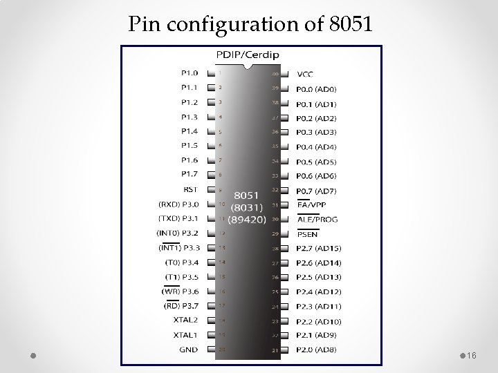
Pin configuration of 8051 16

Port 1 Each of these pins can be configured as an input or an output. Pins 1 -8: Pin 9: RST A logic one on this pin disables the microcontroller and clears the contents of most registers. In other words, the positive voltage on this pin resets the microcontroller. By applying logic zero to this pin, the program starts execution from the beginning. Pins 10 -17: Port 3 Similar to port 1, each of these pins can serve as general input or output. Besides, all of them have alternative functions: Pin 10: RXD Serial asynchronous communication input or Serial synchronous communication output. 17

Pin 11: TXD Serial asynchronous communication output or Serial synchronous communication clock output. Pin 12: INT 0 Interrupt 0 input. Pin 13: INT 1 Interrupt 1 input. Pin 14: T 0 Counter 0 clock input. Pin 15: T 1 Counter 1 clock input. Pin 16: WR Write to external (additional) RAM. Pin 17: RD Read from external RAM. Pin 18, 19: X 2, X 1 Internal oscillator input and output. A quartz crystal which specifies operating frequency is usually connected to these pins. Pin 20: GND Ground. 18

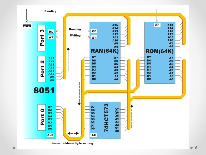
Pin 21 -28: Port 2 If there is no intention to use external memory then these port pins are configured as general inputs/outputs. In case external memory is used, the higher address byte, i. e. addresses A 8 A 15 will appear on this port. Even though memory with capacity of 64 Kb is not used, which means that not all eight port bits are used for its addressing, the rest of them are not available as inputs/outputs. Pin 29: PSEN (Program Store Enable) it is an output pin which is used to access external ROM containing the program code. Pin 30: ALE (Address Latch Enable) Prior to reading from external memory, the microcontroller puts the lower address byte (A 0 -A 7) on P 0 and activates the ALE output. After receiving signal from the ALE pin, the external register memorizes the state of P 0 and uses it as a memory chip address. Immediately after that, the ALU pin is returned its previous logic state and P 0 is now used as a Data Bus. As seen, port data multiplexing is performed by means of only one additional integrated circuit. In other words, this port is used for both data and address transmission. 19

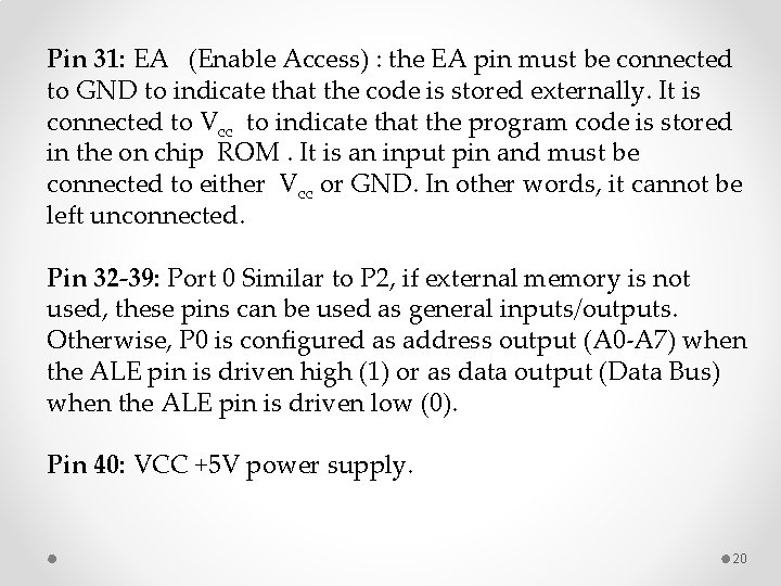
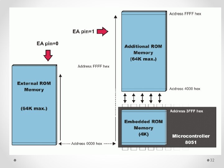
Pin 31: EA (Enable Access) : the EA pin must be connected to GND to indicate that the code is stored externally. It is connected to Vcc to indicate that the program code is stored in the on chip ROM. It is an input pin and must be connected to either Vcc or GND. In other words, it cannot be left unconnected. Pin 32 -39: Port 0 Similar to P 2, if external memory is not used, these pins can be used as general inputs/outputs. Otherwise, P 0 is configured as address output (A 0 -A 7) when the ALE pin is driven high (1) or as data output (Data Bus) when the ALE pin is driven low (0). Pin 40: VCC +5 V power supply. 20

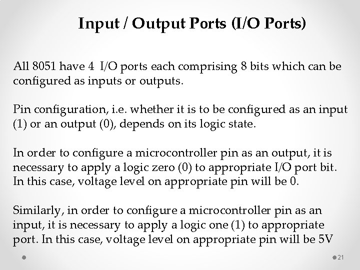
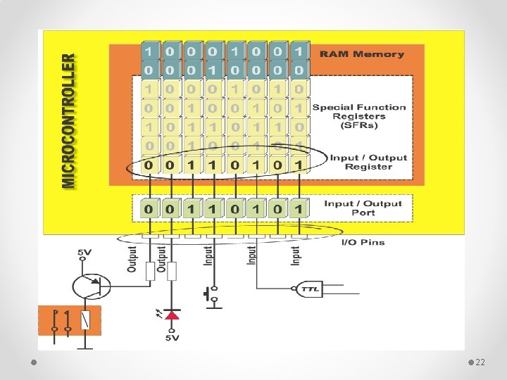
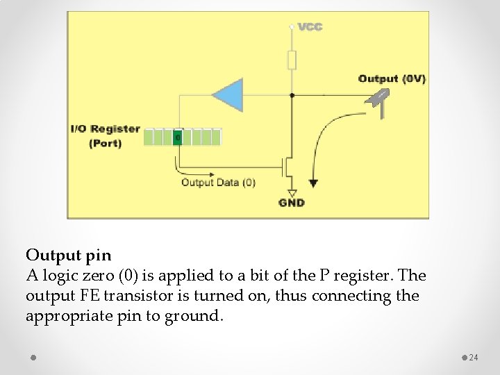
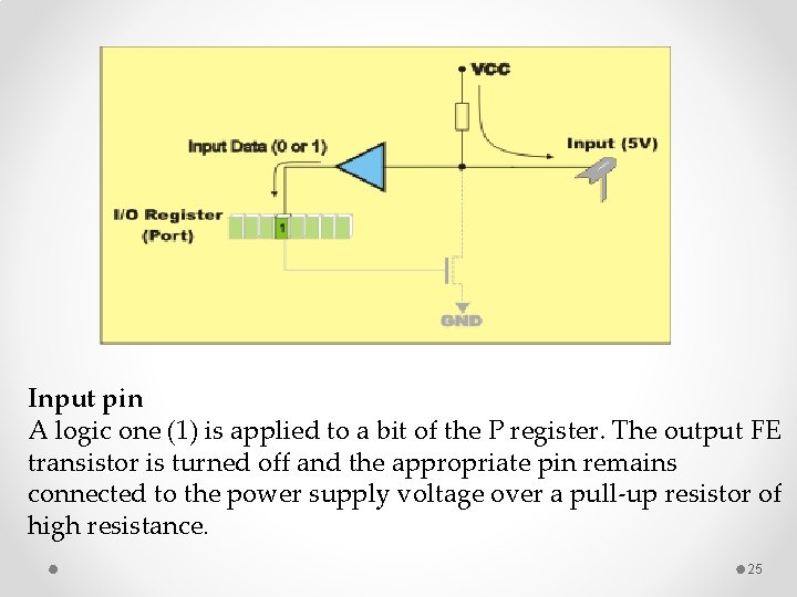
Input / Output Ports (I/O Ports) All 8051 have 4 I/O ports each comprising 8 bits which can be configured as inputs or outputs. Pin configuration, i. e. whether it is to be configured as an input (1) or an output (0), depends on its logic state. In order to configure a microcontroller pin as an output, it is necessary to apply a logic zero (0) to appropriate I/O port bit. In this case, voltage level on appropriate pin will be 0. Similarly, in order to configure a microcontroller pin as an input, it is necessary to apply a logic one (1) to appropriate port. In this case, voltage level on appropriate pin will be 5 V 21

22

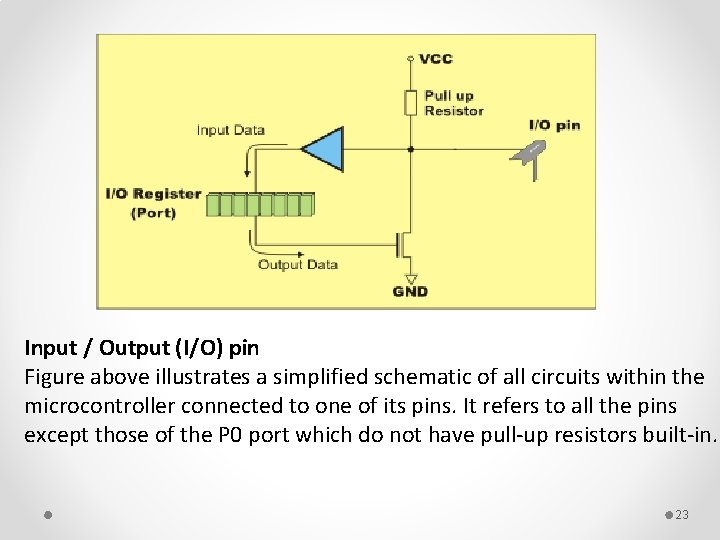
Input / Output (I/O) pin Figure above illustrates a simplified schematic of all circuits within the microcontroller connected to one of its pins. It refers to all the pins except those of the P 0 port which do not have pull-up resistors built-in. 23

Output pin A logic zero (0) is applied to a bit of the P register. The output FE transistor is turned on, thus connecting the appropriate pin to ground. 24

Input pin A logic one (1) is applied to a bit of the P register. The output FE transistor is turned off and the appropriate pin remains connected to the power supply voltage over a pull-up resistor of high resistance. 25

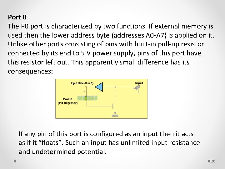
Port 0 The P 0 port is characterized by two functions. If external memory is used then the lower address byte (addresses A 0 -A 7) is applied on it. Unlike other ports consisting of pins with built-in pull-up resistor connected by its end to 5 V power supply, pins of this port have this resistor left out. This apparently small difference has its consequences: If any pin of this port is configured as an input then it acts as if it “floats”. Such an input has unlimited input resistance and undetermined potential. 26

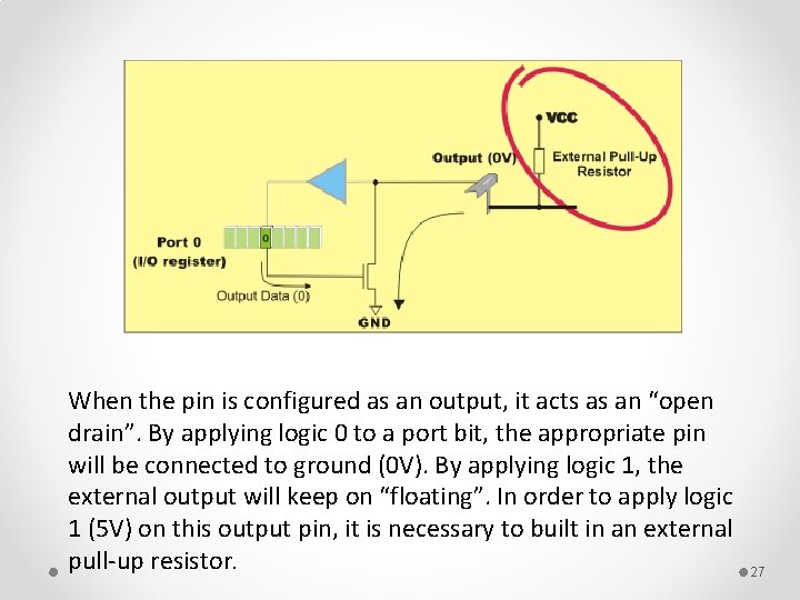
When the pin is configured as an output, it acts as an “open drain”. By applying logic 0 to a port bit, the appropriate pin will be connected to ground (0 V). By applying logic 1, the external output will keep on “floating”. In order to apply logic 1 (5 V) on this output pin, it is necessary to built in an external pull-up resistor. 27

Port 1 P 1 is a true I/O port, because it doesn't have any alternative functions as is the case with P 0, but can be configured as general I/O only. Port 2 P 2 acts similarly to P 0 when external memory is used. Pins of this port occupy addresses intended for external memory chip. This time it is about the higher address byte with addresses A 8 -A 15. When no memory is added, this port can be used as a general input/output port showing features similar to P 1. 28

Port 3 All port pins can be used as general I/O. In order to use the alternative functions, a logic one (1) must be applied to appropriate bit of the P 3 register. In terms of hardware, this port is similar to P 0, with the difference that its pins have a pull-up resistor built-in. 29

Memory Organization • The 8051 has two types of memory and these are Program Memory and Data Memory. • Program Memory (ROM) is used to permanently save the program being executed, while Data Memory (RAM) is used for temporarily storing data and intermediate results created and used during the operation of the microcontroller. • All 8051 microcontrollers have a 16 -bit addressing bus and are capable of addressing 64 kb memory 30

Program Memory The first models of the 8051 microcontroller family did not have internal program memory. It was added as an external separate chip. These models are recognizable by their label beginning with 803 (for example 8031 or 8032). All later models have a few Kbyte ROM embedded. Even though such an amount of memory is sufficient for writing most of the programs, there are situations when it is necessary to use additional memory as well. 31

32

EA=0 In this case, the microcontroller completely ignores internal program memory and executes only the program stored in external memory. EA=1 In this case, the microcontroller executes first the program from built-in ROM, then the program stored in external memory. In both cases, P 0 and P 2 are not available for use since being used for data and address transmission. Besides, the ALE and PSEN pins are also used. 33

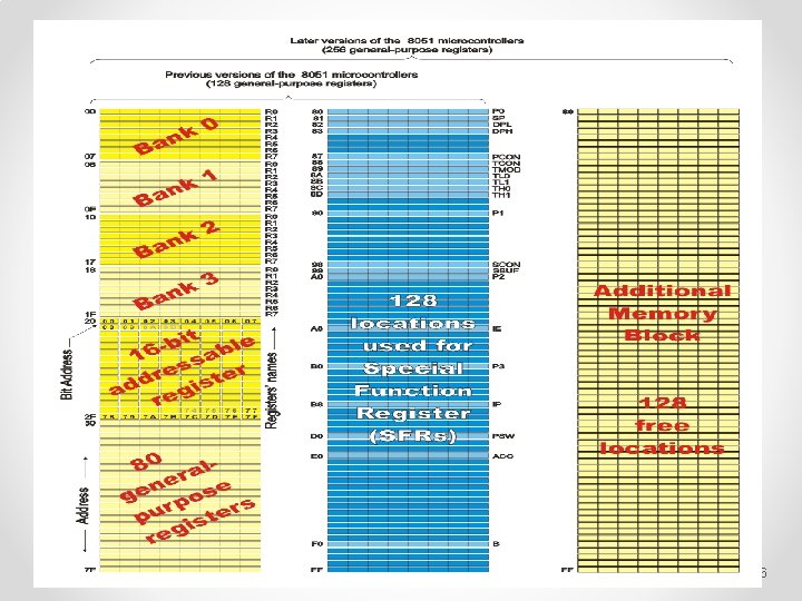
Data Memory is used for temporarily storing data and intermediate results created and used during the operation of the microcontroller. Locations available to the user occupy memory space with addresses 0 -7 Fh, i. e. first 128 registers. The next memory block (address 20 h-2 Fh) is bitaddressable, which means that each bit has its own address (0 -7 Fh). Since there are 16 such registers, this block contains in total of 128 bits with separate addresses (address of bit 0 of the 20 h byte is 0, while address of bit 7 of the 2 Fh byte is 7 Fh). The third group of registers occupy addresses 2 Fh-7 Fh, i. e. 80 locations, and does not have any special functions or features. 34

Additional RAM The additional memory block shares the same addresses with locations intended for the SFRs (80 h- FFh). In order to differentiate between these two physically separated memory spaces, different ways of addressing are used. The SFRs memory locations are accessed by direct addressing, while additional RAM memory locations are accessed by indirect addressing. 35

36

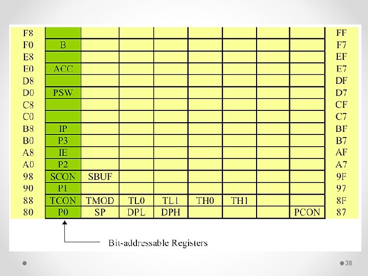
Special Function Registers (SFRs) are a sort of control table used for running and monitoring the operation of the microcontroller. Each of these registers as well as each bit they include, has its name, address in the scope of RAM and precisely defined purpose such as timer control, interrupt control, serial communication control etc. Even though there are 128 memory locations intended to be occupied by them, the basic core, shared by all types of 8051 microcontrollers, has only 21 such registers. 37

38

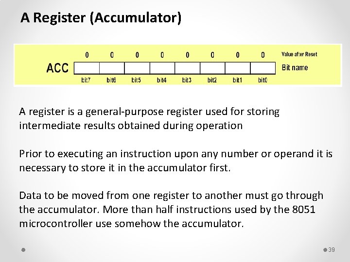
A Register (Accumulator) A register is a general-purpose register used for storing intermediate results obtained during operation Prior to executing an instruction upon any number or operand it is necessary to store it in the accumulator first. Data to be moved from one register to another must go through the accumulator. More than half instructions used by the 8051 microcontroller use somehow the accumulator. 39

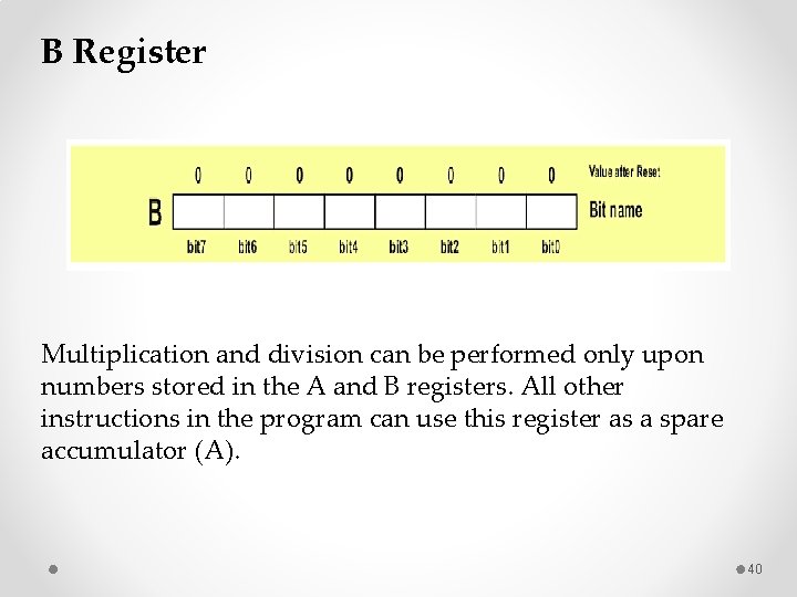
B Register Multiplication and division can be performed only upon numbers stored in the A and B registers. All other instructions in the program can use this register as a spare accumulator (A). 40

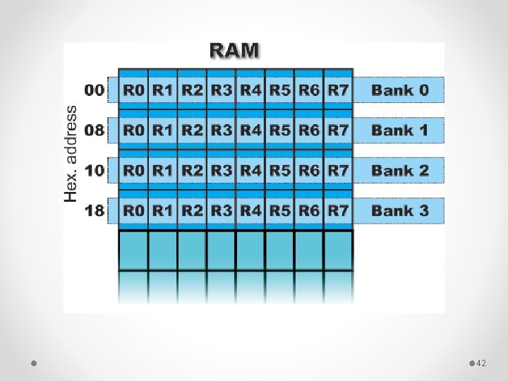
R Registers (R 0 -R 7) This is a common name for 8 general-purpose registers (R 0, R 1, R 2. . . R 7). They occupy 4 banks within RAM. Similar to the accumulator, they are used for temporary storing variables and intermediate results during operation. Which one of these banks is to be active depends on two bits of the PSW Register. Active bank is a bank the registers of which are currently used. 41

42

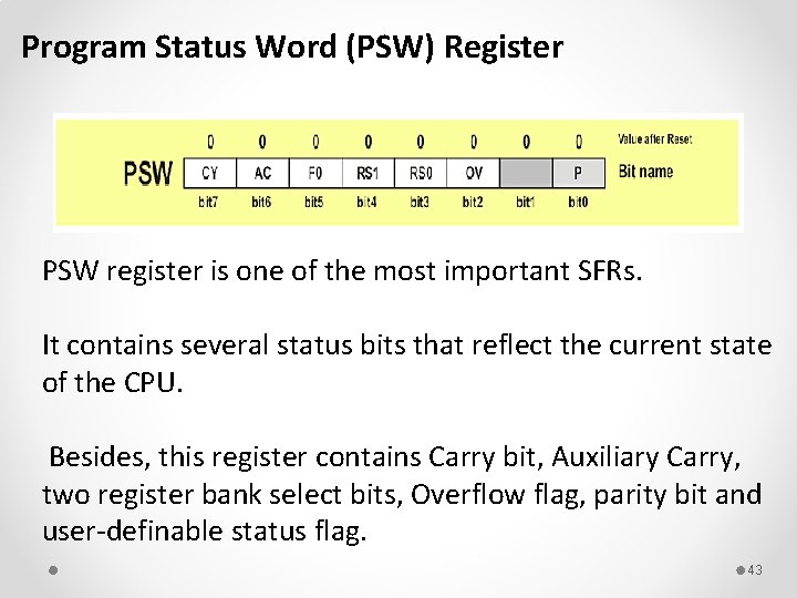
Program Status Word (PSW) Register PSW register is one of the most important SFRs. It contains several status bits that reflect the current state of the CPU. Besides, this register contains Carry bit, Auxiliary Carry, two register bank select bits, Overflow flag, parity bit and user-definable status flag. 43

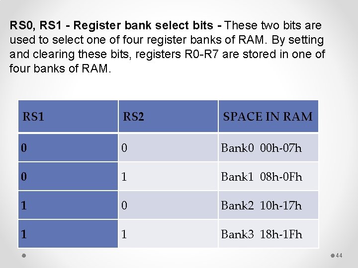
RS 0, RS 1 - Register bank select bits - These two bits are used to select one of four register banks of RAM. By setting and clearing these bits, registers R 0 -R 7 are stored in one of four banks of RAM. RS 1 RS 2 SPACE IN RAM 0 0 Bank 0 00 h-07 h 0 1 Bank 1 08 h-0 Fh 1 0 Bank 2 10 h-17 h 1 1 Bank 3 18 h-1 Fh 44

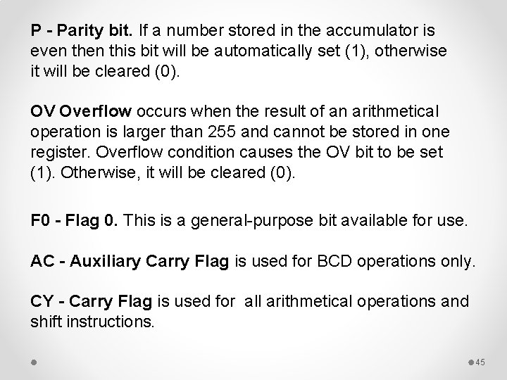
P - Parity bit. If a number stored in the accumulator is even this bit will be automatically set (1), otherwise it will be cleared (0). OV Overflow occurs when the result of an arithmetical operation is larger than 255 and cannot be stored in one register. Overflow condition causes the OV bit to be set (1). Otherwise, it will be cleared (0). F 0 - Flag 0. This is a general-purpose bit available for use. AC - Auxiliary Carry Flag is used for BCD operations only. CY - Carry Flag is used for all arithmetical operations and shift instructions. 45

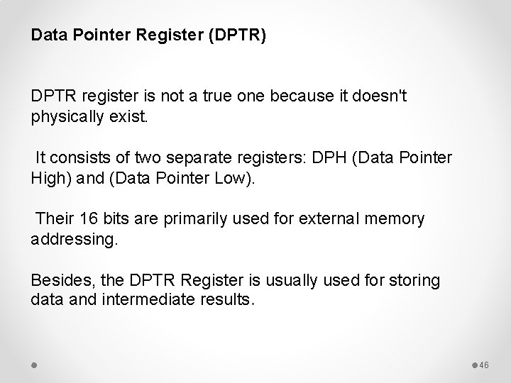
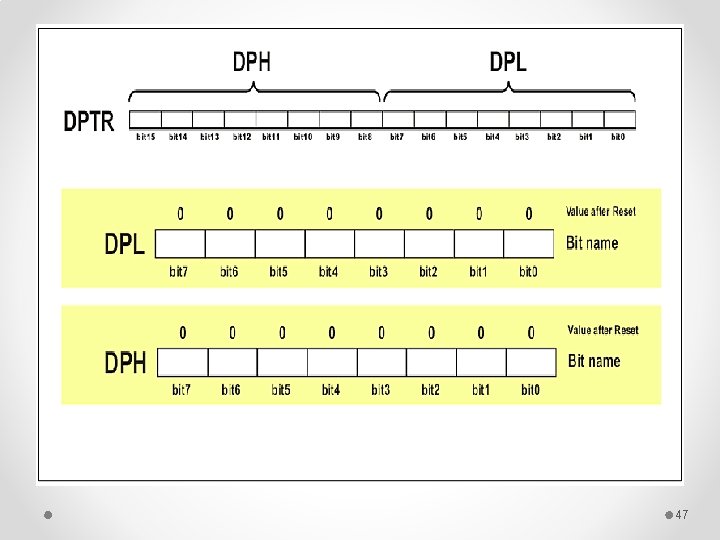
Data Pointer Register (DPTR) DPTR register is not a true one because it doesn't physically exist. It consists of two separate registers: DPH (Data Pointer High) and (Data Pointer Low). Their 16 bits are primarily used for external memory addressing. Besides, the DPTR Register is usually used for storing data and intermediate results. 46

47