MICROCONTROLLERS 8051 Architecture of 8051 Sachin Bhalavat 9409049436

MICROCONTROLLERS 8051

Architecture of 8051
")
Sachin Bhalavat (9409049436)


The 8051 Architecture consist of these specific features Ø The 8 bit CPU with Registers A and B Ø Internal ROM Ø 16 -bit program counter(PC) and data pointer(DPTR) Ø Internal RAM of 128 bytes Ø 8 -bit Program Status word(PSW) Ø Two 16 bit Counter / timers Ø 4 eight-bit ports Ø 3 internal interrupts and 2 external interrupts. Ø Control register Ø Oscillator and clock circuits.

INTERNAL MEMORY
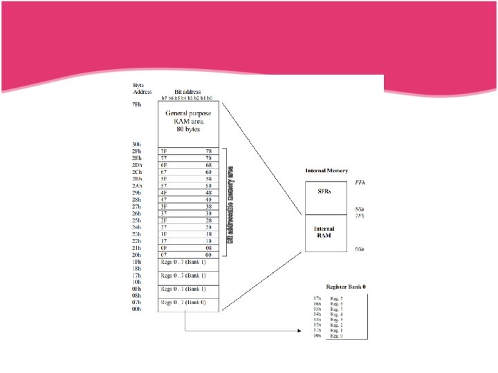

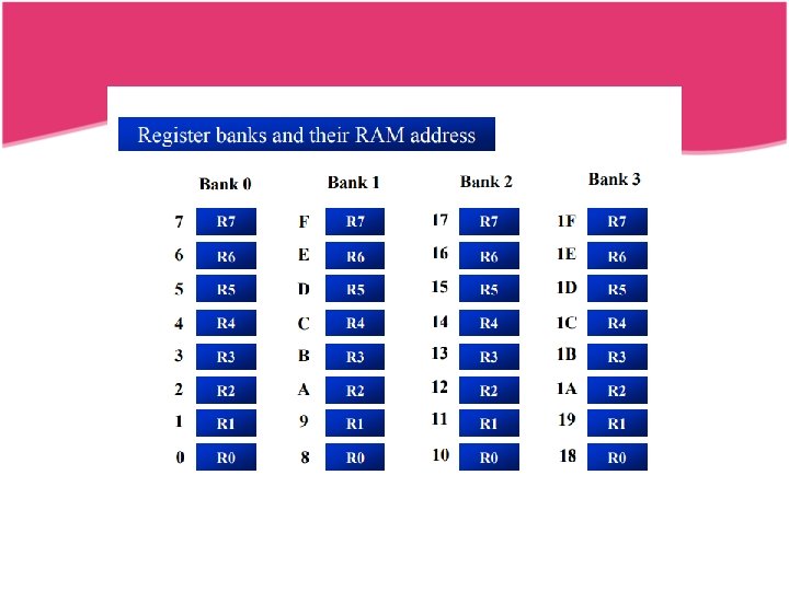
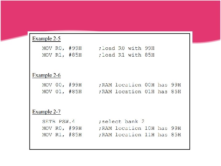
Internal RAM The 128 byte internal RAM shown in figure It is organized into three areas. 1. Working register: Ø Thirty-two bytes from address 00 h to 1 Fh that make up 32 working register organized as Four bank of eight bit each. Ø Bits RS 0 and RS 1 in the PSW determine which bank of register is currently Is use. Ø Bank 0 is selected upon reset 2. Bit addressable: Ø A bit addressable area of 16 bytes occupies RAM bytes addresses 20 h to 2 Fh, forming A total of 128 addressable bits. Ø An addressable bit may be specified by its bit address of 00 h to 7 Fh. 3. General purpose: Ø A general-purpose RAM area above the bit area, form 30 h to 7 Fh, addresable as bytes. Ø A total of 80 bytes from locations 30 H to 7 FH are used for read and write storage, called scratch pad.
")
Internal RAM Organization Sachin Bhalavat (9409049436)

External memory is used in cases when the internal ROM and RAM memory Available On chip is not sufficient. Two separate are made available by the 16 -bit PC and the DPTR and by different control pins for enabling external ROM and RAM chips. If the 128 bytes of internal RAM is insufficient, the external RAM is accessed by the DPTR. In the 8051 family, external RAM of upto 64 KB can be added to any chip.

Register bank

Special function register • 8051 provides 21 SFR and they are for selecting various programmable features of the microcontroller. • Each SFR has an internal one byte address assigned to it. • Some of the registers are both byte and bit addressable.
 ØThe SFR (Special Function Register) can be accessed by their")
Special Function Register (SFR) ØThe SFR (Special Function Register) can be accessed by their names or by their addresses. Ø� The SFR registers have addresses between 80 H and FFH. ØNot all the address space of 80 to FF is used by SFR. ØThe unused locations 80 H to FFH are reserved and must not be used by the 8051 programmer.
")
Special Function Register (SFR)
cont. . Ø CPU registers: - ACC -B - PSW -")
Special Function Register (SFR)cont. . Ø CPU registers: - ACC -B - PSW - SP - DPTR Ø Interrupt control: -IE -IP : Accumulator. : B register. : Program Status Word. : Stack Pointer. : Data Pointer (DPH, DPL). : Interrupt Enable. : Interrupt Priority. Ø I/O Ports: - P 0 - P 1 - P 2 - P 3 : Port 0. : Port 1. : Port 2. : Port 3.
cont. . ØTimers: - TMOD : Timer mode. - TCON :")
Special Function Register (SFR)cont. . ØTimers: - TMOD : Timer mode. - TCON : Timer control. - TH 0 : Timer 0 high byte. - TL 0 : Timer 0 low byte. - TH 1 : Timer 1 high byte. - TL 1 : Timer 1 low byte. ØSerial I/O: - SCON : Serial port control. - SBUF : Serial data registers. ØOther: - PCON : Power control

A and B CPU Register q. The 8051 contains 34 general purpose or working registers. Two of these Register A and B. ØThe immediate result is stored in the accumulator register (Acc) for next operation. ØThe B register is a register just for multiplication and division operation which requires more register spaces for the product of multiplication and the quotient and the remainder for the division.
 ØThe program status store the status of the result of ALU")
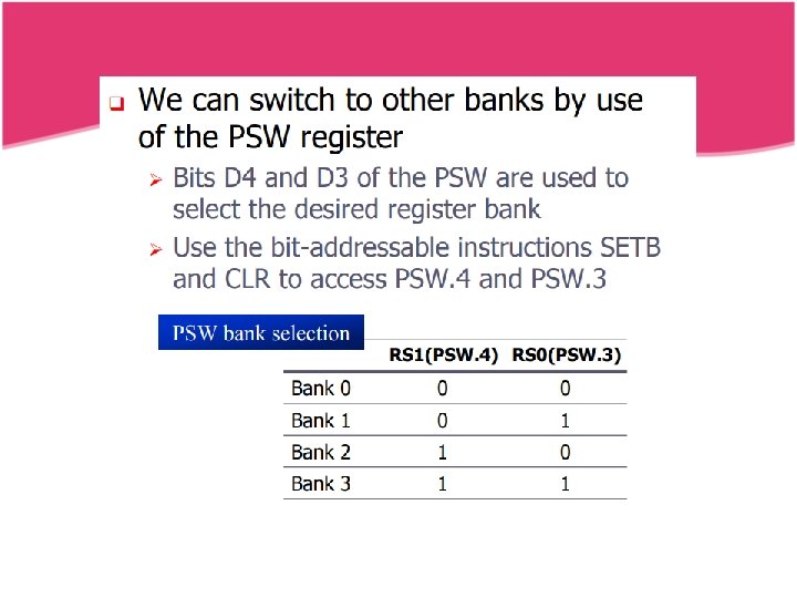
Program status word(PSW) ØThe program status store the status of the result of ALU operations. ØThe PSW contain the math flags, user definable flag and the register select bits that identify which of the four General-purpose register banks is currently in use by the program. ØThe math flags include carry(c), auxiliary carry(AC), overflow(OV) and parity(p)
")
Program Status Word (PSW)

Eg :

Eg: 2
 Ø The program counter points to the address of the next")
Program counter (PC) Ø The program counter points to the address of the next instruction to be Executed Ø As the CPU fetches the opcode from the program ROM, the program counter is increasing to point to the next instruction. Ø The program counter is 16 bits wide Ø This means that it can access program addresses 0000 to FFFFH, a total of 64 K bytes of code
 Ø The data pointer is 16 bit register. Ø It is")
Data pointer (DPTR) Ø The data pointer is 16 bit register. Ø It is used to hold the 16 bit address of the data in the memory. Ø The DPTR register can be accessed separately as lower eight bit(DPL) and higher eight bit (DPH). Ø It can be used as a 16 bit data register or two independent data register.
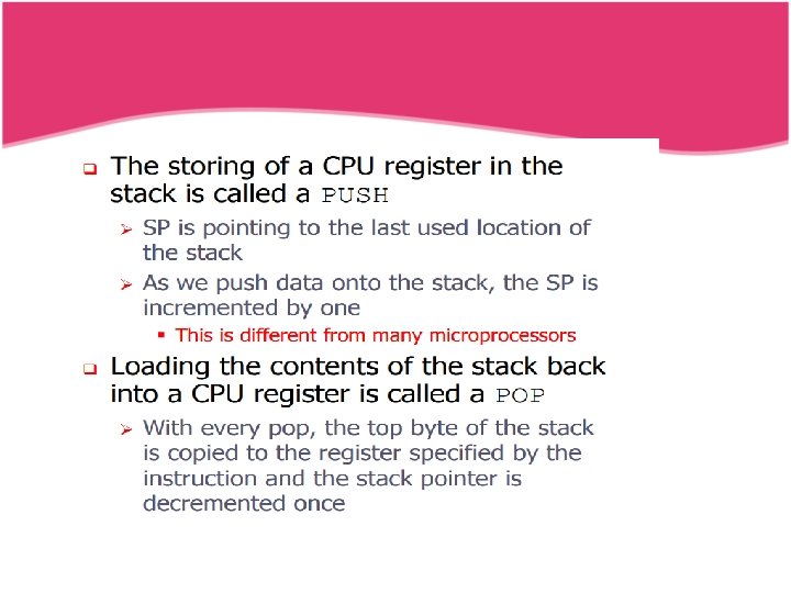
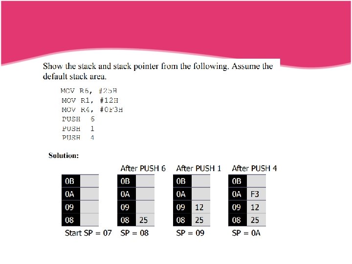
 ØThe stack is a section of RAM")
The stack and The stack pointer (SP) ØThe stack is a section of RAM used by the CPU to store information temporarily ØThis information could be data or an address Ø� The register used to access the stack is called the SP (stack pointer) register ØThe stack pointer in the 8051 is only 8 bit wide.

Operation of stack push pop stack pointer stack

Stack

Timer/Counters

Timer/Counters Ø Two 16 -bit up counters, named T 0 and T 1, are provided for the general use of the programmer. Ø Each counter may be programmed to count internal clock pulses, acting as a timer, or programmed to count external pulses as a counter. Ø The counters are divided into two 8 -bit registers called the timer low (TL 0, TL 1) and high (TH 0, TH 1) bytes. Ø All counter action is controlled by bit states in the timer mode control register (TMOD), the timer/counter control register (TCON) and certain program instructions. ØTMOD is dedicated to the two timers and can be consider two duplicate 4 -bit registers, each of which controls the action of the timers. ØTCON has control bits and flags for the timers in the upper control bits and flags for the external interrupts in the lower nibble.

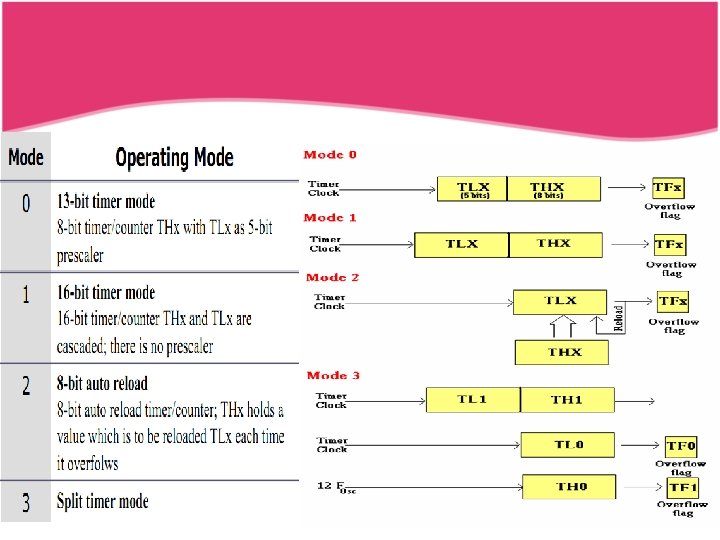
TMOD • Both timers 0 and 1 use the same register, called TMOD (timer mode), to set the various timer operation modes • TMOD is a 8 -bit register • The lower 4 bits are for Timer 0 • The upper 4 bits are for Timer 1 • In each case, • The lower 2 bits are used to set the timer mode • The upper 2 bits to specify the operation

MSB GATE LSB C/T M 1 M 0 GATE Timer 1 C/T M 1 Timer 0 TMOD Register M 0

• • Timers of 8051 do starting and stopping by either software or hardware control In using software to start and stop the timer where GATE=0 – The start and stop of the timer are controlled by way of software by the TR (timer start) bits TR 0 and TR 1 – The SETB instruction starts it, and it is stopped by the CLR instruction – These instructions start and stop the timers as long as GATE=0 in the TMOD register The hardware way of starting and stopping the timer by an external source is achieved by making GATE=1 in the TMOD register C/T : Set for counter operation, reset for timer operation

TMOD

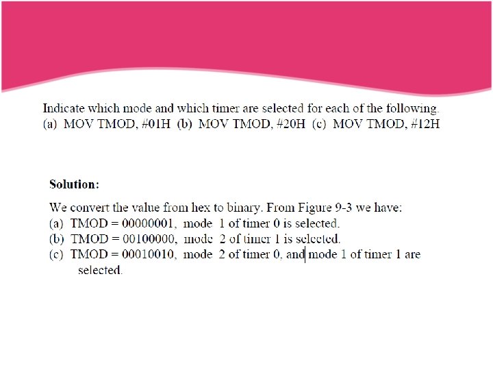
• • • Timers of 8051 do starting and stopping by either software or hardware control In using software to start and stop the timer where GATE=0 – The start and stop of the timer are controlled by way of software by the TR (timer start) bits TR 0 and TR 1 – The SETB instruction starts it, and it is stopped by the CLR instruction – These instructions start and stop the timers as long as GATE=0 in the TMOD register The hardware way of starting and stopping the timer by an external source is achieved by making GATE=1 in the TMOD register Find the value for TMOD if we want to program timer 0 in mode 2, use 8051 XTAL for the clock source, and use instructions to start and stop the timer. TMOD = 0000 0010
 Ø These timers exist in the SFR area as pairs of")
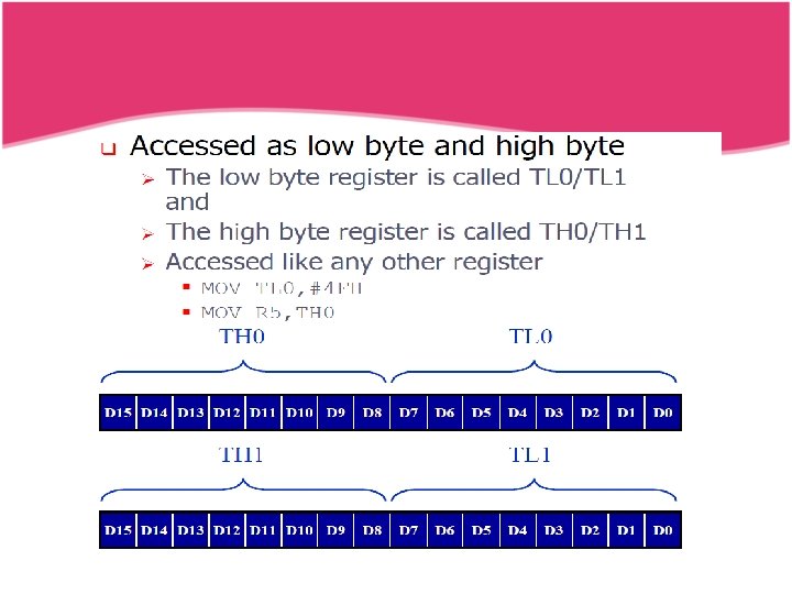
Timer/Counters(cont. . ) Ø These timers exist in the SFR area as pairs of 8 - bit registers. – TL 0 (8 AH) and TH 0 (8 CH) for Timer 0. – TL 1 (8 BH) and TH 1 (8 DH) for Timer 1. (LSB is bit 0 ; MSB is bit 7) Ø When used as timers, the registers are incremented once per machine cycle. – Each machine cycle is 12 clock cycles. Count frequency = (system clock frequency) / 12 ØWhen used as counters, the registers will be incremented once on every 1 -0 (negative edge) on the appropriate input pin. • T 0 – P 3. 4 • T 1 – P 3. 5 ØThe pins must be held high for one complete machine cycle and then low for one complete machine cycle.

Structure of TCON register TF 1 TR 1 TF 0 TR 0 IE 1 - TF 1, TF 0 : Overflow flags for Timer 1 and Timer 0. - TR 1, TR 0 : Run control bits for Timer 1 and Timer 0. Set to run, reset to hold. - IE 1, IE 0 : Edge flag for external interrupts 1 and 0. * Set by interrupt edge, cleared when interrupt is processed. - IT 1, IT 0 : Type bit for external interrupts. * Set for falling edge interrupts, reset for 0 level interrupts. * = not related to counter/timer operation. IT 1 IE 0 IT 0
 TF 1 TR 1 TF 0 TR 0 IE 1")
TCON (Counter/Timer Control Register) TF 1 TR 1 TF 0 TR 0 IE 1 IT 1 IE 0 IT 0 - TF 1, TF 0 : Overflow flags for Timer 1 and Timer 0. - TR 1, TR 0 : Run control bits for Timer 1 and Timer 0. Set to run, reset to hold. - IE 1, IE 0 : Edge flag for external interrupts 1 and 0. * Set by interrupt edge, cleared when interrupt is processed. - IT 1, IT 0 : Type bit for external interrupts. * Set for falling edge interrupts, reset for 0 level interrupts. * = not related to counter/timer operation.

Timer/Counters: Block Schematic

Timer/Counters: Application The timers can be used for: 1. Interval timing The timer is programmed to overflow at a regular interval and set the timer overflow flag. Overflow means reaching maximum count of FFFFH. 2. Event counting Determine the number of occurrences of an event. An event is any external stimulus that provides a 1 -to-0 transition on a pin of the µC.

Pin Description of the 8051 P 1. 0 P 1. 1 P 1. 2 P 1. 3 P 1. 4 P 1. 5 P 1. 6 P 1. 7 RST (RXD)P 3. 0 (TXD)P 3. 1 (INT 0)P 3. 2 (INT 1)P 3. 3 (T 0)P 3. 4 (T 1)P 3. 5 (WR)P 3. 6 (RD)P 3. 7 XTAL 2 XTAL 1 GND Tuesday, January 4, 2022 1 2 3 4 5 6 7 8 9 10 11 12 13 14 15 16 17 18 19 20 8051 40 39 38 37 36 35 34 33 32 31 30 29 28 27 26 25 24 23 22 21 Vcc P 0. 0(AD 0 P ) 0. 1(AD 1) P 0. 2(AD 2 P ) 0. 3(AD 3) P 0. 4(AD 4) P 0. 5(AD 5) P 0. 6(AD 6) P 0. 7(AD 7) EA/VPP ALE/PROG PSEN P 2. 7(A 15) P 2. 6(A 14) P 2. 5(A 13) P 2. 4(A 12) P 2. 3(A 11) P 2. 2(A 10) P 2. 1(A 9) P 2. 0(A 8)

I/O Ports -Four 8 -bit I/O ports. Port 0 Port 1 Port 2 Port 3

• The 8051 microcontroller has four parallel I/O ports , each of 8 -bits. • So, it provides the user 32 I/O lines for connecting the microcontroller to the peripherals. • The four ports are P 0 (Port 0), P 1(Port 1) , P 2(Port 2) and P 3 (Port 3). • Upon reset all the ports are output ports. • In order to make them input, all the ports must be set • i. e a high bit must be sent to all the port pins.

Port 0 • Port 0 is an 8 -bit I/O port with dual purpose. • If external memory is used, these port pins are used for the lower address byte address/data (AD 0 -AD 7), otherwise all bits of the port are either input or output. • Port 0 can also be used as address/data bus(AD 0 -AD 7), allowing it to be used for both address and data. • When connecting the 8051 to an external memory, port 0 provides both address and data. • The 8051 multiplexes address and data through port 0 to save the pins. ALE indicates whether P 0 has address or data. • When ALE = 0, it provides data D 0 -D 7, and when ALE =1 it provides address

Port 1 • Port 1 occupies a total of 8 pins (pins 1 through 8). • It has no dual application and acts only as input or output port. • In contrast to port 0, this port does not need any pull-up resistors since pull-up resistors connected internally. • Upon reset, Port 1 is configured as an output port. • To configure it as an input port , port bits must be set i. e a high bit must be sent to all the port pins. • This is normally done by the instruction ―SETB. • For Ex : MOV A, #0 FFH ; A=FF HEX MOV P 1, A

Port 2 • Port 2 is also an eight bit parallel port. (pins 21 - 28). • It can be used as input or output port. • As this port is provided with internal pull-up resistors it does not need any external pull-up resistors. • Upon reset, Port 2 is configured as an output port. • If the port is to be used as input port, all the port bits must be made high by sending FF to the port. • Port 2 lines are also associated with the higher order address lines A 8 -A 15. • For ex, MOV A, #0 FFH ; A=FF hex MOV P 2, A ; make P 2 an input port by writing all 1’s to it

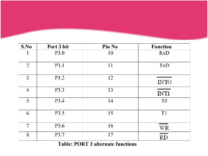
Port 3 • Port 3 is also an 8 -bit parallel port with dual function. ( pins 10 to 17). • The port pins can be used for I/O operations as well as for control operations. • Upon reset port 3 is configured as an output port. • If the port is to be used as input port, all the port bits must be made high by sending FF to the port.
: 1 External Interrupt 0")
Interrupt System Ø 5 Interrupt Sources (in order of priority): 1 External Interrupt 0 (IE 0) 2 Timer 0 (TF 0) 3 External Interrupt 1 (IE 1) 4 Timer 1 (TF 1) 5 Serial Port (RI/TI) Ø Each interrupt type has a separate vector address. Ø Each interrupt type can be programmed to one of two priority levels. Ø External interrupts can be programmed for edge or level sensitivity.

• Upon reset all Interrupts are disabled & do not respond to the Microcontroller. • These interrupts must be enabled by software in order for the Microcontroller to respond to them. • This is done by an 8 -bit register called Interrupt Enable Register (IE). Sachin Bhalavat (9409049436)
")
Sachin Bhalavat (9409049436)

Interrupt vector Addresses Source Address IE 0 03 H TF 0 0 BH IE 1 13 H TF 1 1 BH RI&TI 23 H The 8051 starts execution at 0000 H after Reset.

Interrupt Enable Register

IP: Interrupt Priority Register • Priority can also be set to high or low by 8 -bit IP register- Interrupt priority register

IP: Interrupt Priority Register

Basics of serial communication

Types of Serial communications

Rx. D and Tx. D pins in the 8051 Ø The 8051 has two pins for transferring and receiving data by serial communication. These two pins are part of the Port 3(P 3. 0 &P 3. 1) Ø These pins are TTL compatible and hence they require a line driver to make them RS 232 compatible Ø Serial communication is controlled by an 8 -bit register called SCON register, it is a bit addressable register.

SCON : Serial Control Register

SM 0 , SM 1 Ø These two bits of SCON register determine the framing of data by specifying the number of bits per character and start bit and stop bits. There are 4 serial modes. SM 0 SM 1 0 0 Serial Mode 0 0 1 Serial Mode 1, 8 bit data, 1 stop bit, 1 start bit 1 0 Serial Mode 2 1 1 Serial Mode 3
 also referred as SCON. 4. When it is high,")
REN • REN (Receive Enable) also referred as SCON. 4. When it is high, it allows the 8051 to receive data on the Rx. D pin. So to receive and transfer data REN must be set to 1. When REN=0, the receiver is disabled. This is achieved as below SETB SCON. 4 & CLR SCON. 4
 is the D 1 bit of SCON")
TI , RI • TI (Transmit interrupt) is the D 1 bit of SCON register. When 8051 finishes the transfer of 8 -bit character, it raises the TI flag to indicate that it is ready to transfer another byte. The TI bit is raised at the beginning of the stop bit. • RI (Receive interrupt) is the D 0 bit of the SCON register. When the 8051 receives data serially , via Rx. D, it gets rid of the start and stop bits and places the byte in the SBUF register. Then it raises the RI flag bit to indicate that a byte has been received and should be picked up before it is lost. RI is raised halfway through the stop bit.

The 8051 oscillator and clock ØThe 8051 requires an external oscillator circuit. The oscillator circuit usually runs around 12 MHz. The crystal generates 12 M pulses in one second. ØA machine cycle is minimum amount time must take by simplest machine instruction Ø An 8051 machine cycle consists of 12 crystal pulses (clock cycle). ØThe first 6 crystal pulses (clock cycle) is used to fetch the Opcode and the second 6 pulses are used to perform the operation on the operands in the ALU. ØThis gives an effective machine cycle rate at 1 MIPS (Million Instructions Per Second).

Oscillator circuit and timing
- Slides: 70