UNITVIII 8051 Microcontroller Architecture Register set of 8051


 ACC act as an operand")


 – Port 0 is")
 – Port 2 acts")


")


supported by IBM PC")


 register")


- Slides: 52
UNIT-VIII 8051 Microcontroller Architecture Register set of 8051 Modes of timer operation Serial port operation Interrupt structure of 8051 Memory and I/O interfacing of 8051
Fig 8. 1 Architecture of 8051
P 1. 0 P 1. 1 P 1. 2 P 1. 3 P 1. 4 P 1. 5 P 1. 6 P 1. 7 RST (RXD)P 3. 0 (TXD)P 3. 1 (INT 0)P 3. 2 (INT 1)P 3. 3 (T 0)P 3. 4 (T 1)P 3. 5 (WR)P 3. 6 (RD)P 3. 7 XTAL 2 XTAL 1 GND 1 2 3 4 5 6 7 8 9 10 11 12 13 14 15 16 17 18 19 20 8051 40 39 38 37 36 35 34 33 32 31 30 29 28 27 26 25 24 23 22 21 Vcc P 0. 0(AD 0) P 0. 1(AD 1) P 0. 2(AD 2) P 0. 3(AD 3) P 0. 4(AD 4) P 0. 5(AD 5) P 0. 6(AD 6) P 0. 7(AD 7) EA/VPP ALE/PROG PSEN P 2. 7(A 15) P 2. 6(A 14) P 2. 5(A 13) P 2. 4(A 12) P 2. 3(A 11) P 2. 2(A 10) P 2. 1(A 9) P 2. 0(A 8) Fig 8. 2 Pin Description Of 8051
Register set of 8051 1. Accumulator (ACC or A) ACC act as an operand register, in case of some instructions. The ACC register, has been allotted an address in the on-chip special function register bank. 2. B-Register This register is used to store one of the operands for multiply and divide instructions. (In other instruction it is used as a scratch pad. ) This register is considered as a special function register. 3. PSW-Program Status Word This set of flags contains the status information and is considered as one of the special function register.
4. SP-Stack Pointer This 8 -bit wide register is incremented before the data is stored onto the stack using push or call instructions. This register contains 8 -bit stack top address. Stack may be defined anywhere in the on-chip 128 -byte RAM. SP reg. initialized to 07. After each stack output it is incremented. 5. DTPR (Data Pointer) This 16 -bit register contain 16 -bit external data RAM address. DPH -- is higher byte DPL – is lower byte
6. Port 0 to 3 Latches & Drivers These are allotted to I/O ports. These latches have been allotted addresses in the special function register bank using this addresses user can communicate with these ports i. e P 0, P 1, P 2, P 3. 7. Serial Data Buffer The serial data buffer internally contains two independent registers. One register is a transmit buffer which is a parallel-in serialout register. Other register is a receiver buffer which is a serial-in parallel-out register. The serial data buffer is identified as SBUF and is one of the special function registers.
8. Timer Registers These two 16 -bit registers can be accessed as their lower & upper bytes i. e Register 0 – TL 0, TH 0 Register 1 – TL 1, TH 1 All these register can be accessed using the 4 address allotted to them which lie in the SFR address range i. e 80 h to FFh. 9. Control Registers The special function registers IP, IE, TMOD, TCON, SCON & PCON contain control and status information for interrupts, timers, counters and serial port. 10. Timing & Control unit This unit derives all the necessary timing and control signals required for the internal operation of the circuit. It also derives control signals required for controlling the external system bus.
11. Instruction Register This register decodes the opcode of an instruction to be executed and gives information to the timing and control unit to generate necessary signals for the execution of the instruction. 12. EPROM and Program Address Register (PAR) These blocks provide an on-chip EPROM & a mechanism to internally address it (it is not in 8051). 13. RAM & RAM Address Registers These blocks provide internal 128 bytes of RAM and a mechanism to internally address it.
14. ALU TMP 1 & TMP 2 holds the operands, users cannot access. 15. SFR Register Bank This is a set of SFRs(special function registers), which can be addressed using their respective address which lie in the range 80 h to FFh.
Signals description of 8051 Vcc -- +5 v power supply Vss -- ground Reset – It resets the 8051. It is an input pin and is active high The high pulse must be high at least 2 machine cycles. Upon applying a higwill h pulse to RST, the microcontroller will reset and all values in registers be lost. ALE/PROG – ALE is valid only for external memory accesses. This pin acts as program pulse input during onchip EPROM programming. ALE may be used for external timing and clocking purpose. One ALE pulse is skipped during each access to external data memory. The ALE pin is used for de-multiplexing the address and data by
EA – External Access Enable pin If it is low – indicates that the 8051 can address external program memory. If it is high – indicates execution of programs in internal memory. This pin also receives 21 volts for programming of the onchip EPROM. PSEN (Program Store Enable) – it is an active low output signal that acts as a strobe to read the external program memory. This goes low during external program memory accesses.
Port 0 (P 0. 0 – P 0. 7) – Port 0 is an 8 -bit bidirectional bit addressable I/O port. This has been allotted on address in the SFR address range. Port 0 acts as multiplexed address/data lines during external memory access, i. e. when EA is and ALE emits a valid signal. In case of controllers with on-chip EPROM Port 0 receives code bytes during programming of the internal EPROM. Port 1 (P 1. 0 – P 1. 7) – Port 1 acts as an 8 -bit bidirectional bit addressable. This has been allotted an address in the SFR address range.
Port 2 (P 2. 0 – P 2. 7) – Port 2 acts as an 8 -bit bidirectional bit addressable. This has been allotted an address in the SFR address range. During external memory access, ports emits higher eight bits of address(A 8 -A 15) which are valid, if ALE goes high and EA is low. P 2 also receives higher order address bits during programming of the on-chip EPROM. Port 3 (P 3. 0 – P 3. 7) – Port 3 acts as an 8 -bit bidirectional bit addressable. This has been allotted an address in the SFR address range. The port 3 pins also serve the alternative functions.
• XTAL 1 & XTAL 2 -- There is an inbuilt oscillator which derives the necessary clock frequency for the operation of the controller. XTAL 1 – is the input of the amplifier XTAL 2 – is the output of the amplifier
Port 3 pins Alternative Function P 3. 0 Acts as serial input data pin (RXD) P 3. 1 Acts as serial output data pin (TXD) P 3. 2 Acts as external interrupt pin 0 (INT 0) P 3. 3 Acts as external interrupt pin 1 (INT 1) P 3. 4 Acts as external input to timer 0 (T 0) P 3. 5 Acts as external input to timer 1 (T 1) P 3. 6 Acts as write control signal for external data memory write operation (WR) P 3. 7 Acts as read control signal for external data memory read operation (RD) Table 8. 1 Alternate Functions of Pins of Port 3
Addressing Modes Immediate Register Direct Register indirect Indexed
Immediate Addressing Mode MOV A, #25 H ; load 25 H into A MOV R 4, #62 ; load the decimal value 62 into R 4 MOV B, #40 H ; load 40 H into B MOV DPTR, #4521 H; DPTR=4521 H MOV DPTR, #2550 H ; is the same as: MOV DPL, #50 H MOV DPH, #25 H
Register Addressing Mode MOV ADD MOV A, R 0 R 2, A A, R 5 A, R 7 R 6, A ; copy the contents of R 0 into A ; copy the contents of A into R 2 ; add the contents of R 5 to contents of A ; add the contents of R 7 to contents of A ; save accumulator in R 6 MOV DPTR, #25 F 5 H MOV R 7, DPL MOV R 6, DPH
Direct Addressing Mode MOV R 0, 40 H in R 0 MOV 56 H, A MOV R 4, 7 FH to R 4 MOV A, 7 MOV A, R 7 ; save content of RAM location ; save content of A in RAM location 56 H ; move contents of RAM location ; is same as ; which means copy R 4 into A ; is same as ; which means copy R 7 into A
Register Indirect Addressing Mode MOV A, @R 0 MOV @R 1, B ; move contents of RAM location whose ; address is held by R 0 into A ; move contents of B into RAM location ; whose address is held by R 1
Index Addressing Mode DPTR: 16 bits MOVC A, @A+DPTR ; “C” means program (code) space ROM
Fig 8. 3 TMOD Register
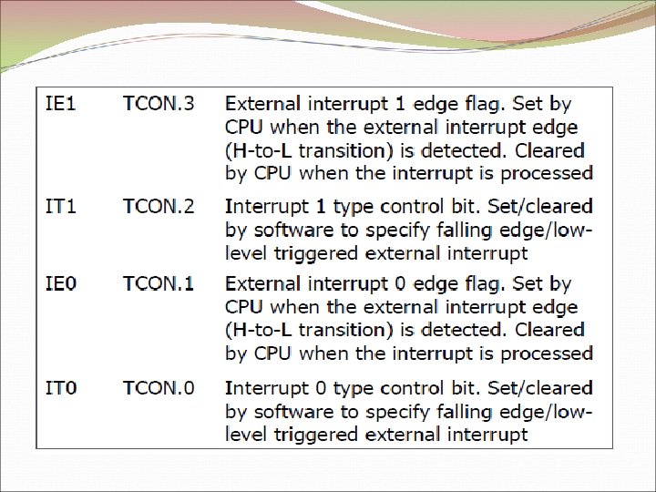
Fig 8. 4 TCON register
Fig 8. 5 Basics of serial communication
Fig 8. 6 Types of serial communication
Fig 8. 7 Asynchronous frame format
Fig 8. 8 RS-232 25 -pin standard
Fig 8. 9 RS-232 9 -pin standard
Fig 8. 10 TTL to RS-232 Conversions
Fig 8. 11 BAUD Rates(Bps)supported by IBM PC
SCON is an 8 -bit register used to program the start bit, stop bit, and data bits of data framing, among other things Fig 8. 12 SCON Register
SBUF is an 8 -bit register used solely for serial communication • For a byte data to be transferred via the Tx. D line, it must be placed in the SBUF Register • The moment a byte is written into SBUF, it is framed with the start and stop bits and transferred serially via the Tx. D line • SBUF holds the byte of data when it is received by 8051 Rx. D line • When the bits are received serially via Rx. D, the 8051 deframes it by eliminating the stop and start bits, making a
Fig 8. 13 PCON Register When 8051 is powered up, SMOD is zero • We can set it to high by software and thereby double the baud rate
Interrupts of 8051 An interrupt is an external or internal event that interrupts the microcontroller to inform it that a device needs its service Polling can monitor the status of several devices and serve each of them as certain conditions are met
Interrupt sequence It finishes the instruction it is executing and saves the address of the next instruction (PC) on the stack 2. It also saves the current status of all the interrupts internally (i. e: not on the stack) 3. It jumps to a fixed location in memory, called the interrupt vector table, that holds the address of the ISR 4. The microcontroller gets the address of the ISR from the interrupt vector table and jumps to it 5. Upon executing the RETI instruction, the microcontroller returns to the place where it was interrupted 1.
Types of 8051 interrupts Reset – power-up reset Two interrupts are set aside for the timers: one for timer 0 and one for timer 1 Two interrupts are set aside for hardware external interrupts P 3. 2 and P 3. 3 are for the external hardware interrupts INT 0 (or EX 1), and INT 1 (or EX 2) Serial communication has a single interrupt that belongs to both receive and transfer
Fig 8. 14 Interrupt vector table
Fig 8. 15 IE (interrupt enable) register
To enable an interrupt, we take the following steps: 1. Bit D 7 of the IE register (EA) must be set to high to allow the rest of register to take effect 2. The value of EA If EA = 1, interrupts are enabled and will be responded to if their corresponding bits in IE are high If EA = 0, no interrupt will be responded to, even if the associated bit in the IE register is high
Fig 8. 16 Interrupts flag bits
Fig 8. 17 Interrupt Priorities upon reset We can alter the sequence of interrupt priority by assigning a higher priority to any one of the interrupts by programming a register called IP (interrupt priority)
Fig 8. 18 Interrupt priority register
There are different types of read-only memory PROM EEPROM Flash EPROM Mask ROM
The 8031 chip is a ROM less version of the 8051 It is exactly like any member of the 8051 family as far as executing the instructions and features are concerned, but it has no on-chip ROM To make the 8031 execute 8051 code, it must be connected to external ROM memory containing the program code
Fig 8. 19 Interfacing 8031 to external ROM
Fig 8. 20 Interfacing 8031 with external data ROM and program ROM
Fig 8. 21 Interfacing 8051 with external ROM
Fig 8. 22 8051 interfacing with 8255
Fig 8. 23 8051 connection to the 8255
Fig 8. 24 8031 Connection to External Program ROM and the 8255
Fig 8. 25 8255 Connection to Stepper Motor