History of 8051 microcontroller In the year 1980


 Ø 8 -bit Ø responsible for performing arithmetic &")
 Ø 8 -bit register Ø Used for performing arithmetic & logical")

 Ø Used to access external data or code Ø 16 bit")

 v Also called as Flag register v 8 -bit reg.")
 ; carry generate from D 7 bit")
 Ø AC = 1; Carry generate from D 3")
 Flag Ø Even parity, Odd parity Ø count number of 1’s in")
 Flag Ø Set whenever high ordered bit to overflow into the sign")
 Flag is set to 1: 1) If there is carry from D")
 Ø 16 -bit register Ø Used to store the address of")
 Stack: - Space at which data are store temporary during the")
 type register Ø The storing CPU register in")


 and data.")


 F 8 F 0 FF B F 7 E 8")


: - Reset v Input pin and active high signal (Normally Low) v")


:External access ü “/” means active low. ü Connected to GND to indicate")
:Address latch enable Ø It is an output and active high pin. Ø")
")


 Internal CPU")


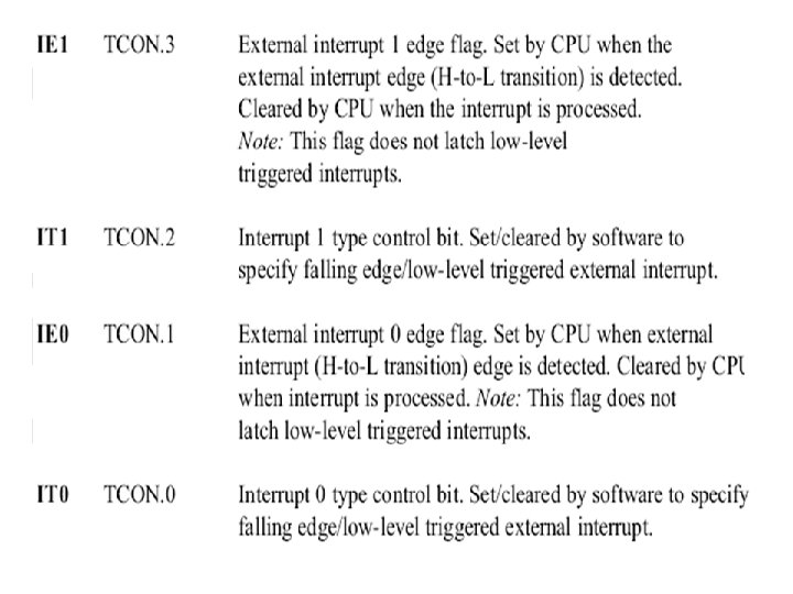
 TF (1 Bit) T Pin TR")
")
 GATE C/T’ M 1 Timer 1 M 0 GATE C/T’ M 1 Timer")

 C/T’ = 0; Timer Operation (Timer 1/0 counts divided down system clock)")

")


 register 70")

 Ø REN (Receive Enable) also referred as SCON. 4. Ø When")
 • It is the D 1 bit of SCON register. •")
 • It is the D 0 bit of the SCON register.")


 The microcontroller gets the address of ISR from interrupt vector table and jump")
 None")
- Slides: 82
History of 8051 microcontroller • In the year 1980 Intel corporation introduced an 8 bit microcontroller called 8051. • It has 4 K bytes of ROM, 128 Bytes of RAM , a serial port, two 16 -bit Timers and 32 I/O pins. • CPU can work with 8 bit of data at a time. • Crystal frequency 12 Mhz to 32 Mhz • Data larger than 8 bit can be broken into 8 bit pieces to be processed by the CPU 2
Features of 8051 ü 8 bit microcontroller ü High-performance CMOS Technology ü Address bus is of 16 bit & data bus is of 8 bit ü 4 K bytes internal ROM (program) ü 128 bytes internal RAM (data) ü 64 K external code & data memory space ü Four 8 -bit I/O ports ü Two 16 -bit timers/counters (Timer 0/ Timer 1)
ü Multiple internal and external interrupt sources ü Serial Port ü Full duplex UART ü Low-power Idle and Power-down Modes
Block diagram of 8051
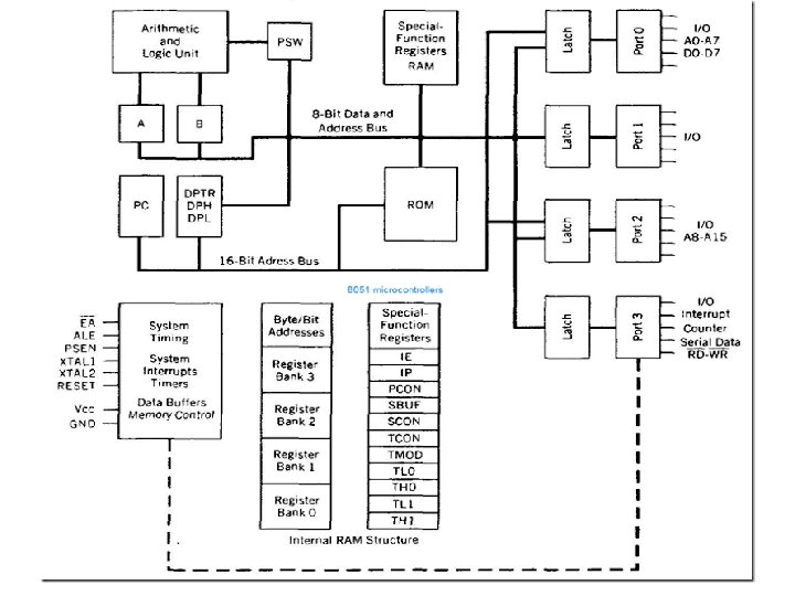
BLOCK DIAGRAM OF 8051 Interrupt Control 4 K ROM Timer 0 128 RAM Timer 1 CPU OSC Bus Control Serial Port 4 I/O Ports P 0 P 1 P 2 P 3 TXD RXD
ALU (Arithmetic & logical unit) Ø 8 -bit Ø responsible for performing arithmetic & logical operation of 8051 Ø size of controller depends on size of ALU (IF ALU is 8 -bit then controller is 8 -bit)
Reg. A (Accumulator) Ø 8 -bit register Ø Used for performing arithmetic & logical operation in ALU Ø Store result after performing arithmetic & logical operation Ex: - Add two 8 -bit numbers. INPUT (BEFORE EXECUTION) A = 05 h B = 04 h OUTPUT (AFTER EXECUTION) A = 09 h
Reg. B Ø 8 -bit register Ø Used with reg. A to perform multiplication and division operation Ø MUL AB: multiplies 8 bit unsigned values in A and B. and leaves the 16 bit result in A (low byte) and B (high byte) Ø DIV AB: divided A by B, leaving the integer result in A and remainder in B
Data pointer (DPTR) Ø Used to access external data or code Ø 16 bit register at addresses 82 H (low byte) and 83 H (high byte) Ø Used in operations regarding external RAM and some instructions involving code memory Ø Also used as 8 -bit reg. DPTR (16) DPH (8) DPL (8) 11
Ex: - Write 55 H into external RAM location 1000 H. MOV A, #55 H MOV DPTR, #1000 H MOVX @DPTR, A
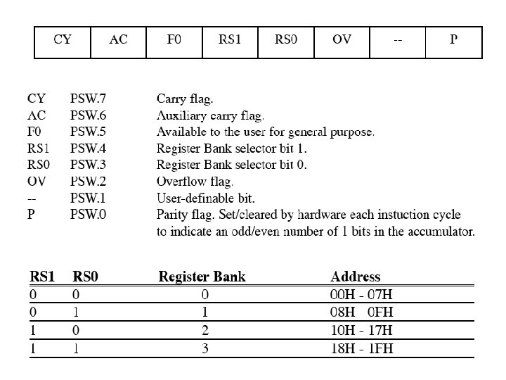
PSW (Program Status Word) v Also called as Flag register v 8 -bit reg. v Indicates status of result after performing the operation v Containing 4 conditional flag
Cy flag: Ø Cy = 1 (set) ; carry generate from D 7 bit Ø Cy = 0 (Reset); no carry from D 7 bit Ex: - D 7 D 6 D 5 D 4 D 3 CY CY = 1 D 0 1 D 1 1 0 0 1 0 D 2 + 1 1 0 0 1 0 RES 1) 0 1 1 1 0 0 D 7 D 6 D 5 D 4 D 3 D 2 D 1 D 0 CY CY = 0 D 2 1 D 2 RES + 1 0 1 1 0 0 1 0 0 1 1 1 0 0
AC flag (Auxiliary Carry Flag) Ø AC = 1; Carry generate from D 3 bit Ø AC = 0; no carry generate from D 3 bit Ø Used for BCD (Binary Coded Decimal) numbers AC = 1 D 7 D 6 D 5 D 4 D 3 CY 1 1 D 1 1 0 1 1 1 D 2 D 1 D 0 0 1 D 2 + 1 1 0 0 1 0 RES 1) 1 0 0
P (Parity) Flag Ø Even parity, Odd parity Ø count number of 1’s in result to check parity P = 1; odd number of 1’s P = 0; Even number of 1’s D 7 CY D 5 1 D 1 P=1 D 6 D 4 D 3 D 2 D 1 D 0 1 1 0 1 D 2 + 1 0 1 0 RES 1) 0 1 0 1 1 1 Note: - only count 1’s in 8 -bit result
OV (Overflow) Flag Ø Set whenever high ordered bit to overflow into the sign bit. Ø CY flag used to detect error in unsigned arithmetic operation. Ø OV flag used to detect error in signed arithmetic operation.
OV (Overflow) Flag is set to 1: 1) If there is carry from D 6 to D 7 and no carry from D 7 out. 2) If there is carry from D 7 out and no carry from D 6 to D 7. (If there is carry both from D 7 out and D 6 to D 7, OV = 0)
PC (Program Counter) Ø 16 -bit register Ø Used to store the address of next instruction to be execute Ø increment by 1 after execution of instruction Ø FIFO (First In First Out) type register
SP (Stack pointer) Stack: - Space at which data are store temporary during the execution of program Ø The register used to access the stack is called SP (stack pointer) register. Ø 8 -bit register Ø Stack operations include pushing data on the stack and popping data off the stack. Ø When 8051 powered up, the SP register contains value 07 h.
Ø LIFO (Last In First Out) type register Ø The storing CPU register in the stack is called a PUSH and pulling the contents off the stack back into CPU register is called POP. Ex. : - MOV R 6, #25 H MOV R 1, #12 H PUSH 6 PUSH 1
Ex. : - MOV R 6, #25 H MOV R 1, #12 H PUSH 6 PUSH Initial 1 After PUSH 6 After PUSH 1 0 B 0 B 0 B 0 A 0 A 0 A 09 09 09 12 08 08 08 25 SP = 07 25 SP = 08 SP = 09
Ex. : - POP 1 POP 5 Initial After POP 1 After POP 5 0 B 0 B 0 B 0 A 0 A 0 A 09 09 12 09 08 25 08 SP = 09 25 SP = 08 08 SP = 07
Internal Memory Ø 8051 implements a separate memory space for programs (code) and data. Ø Internal memory consists of on-chip ROM and onchip data RAM. MEMORY Internal External RAM 128 byte 64 KB ROM 4 KB 64 KB 25
26
Register banks in the 8051 Microcontroller 27
SFR (Special Function Register) F 8 F 0 FF B F 7 E 8 E 0 EF Acc E 7 D 8 D 0 DF PSW D 7 C 8 CF C 0 C 7 B 8 IP BF B 0 P 3 B 7 A 8 IE AF A 0 P 2 A 7 98 SCON 90 P 1 88 TCON TMOD TL 0 TL 1 80 P 0 SP DPL DPH SBUF 9 F 97 TH 0 TH 1 8 F PCON 87
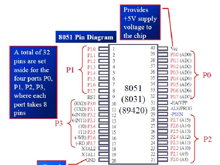
8051 pin Diagram
Oscillator Connection to 8051 ü Using a quartz crystal oscillator ü Crystal frequency = 11. 0592 Mhz C 2 XTAL 2 30 p. F C 1 XTAL 1 30 p. F GND
RST(pin 9): - Reset v Input pin and active high signal (Normally Low) v The high pulse must be high at least 2 machine cycles to Reset the microcontroller. v Power-on reset v During reset all values in registers will be lost.
Power-On RESET Circuit Vcc + 10 u. F 31 30 p. F 8. 2 K 30 p. F 11. 0592 MHz 19 18 EA/VPP X 1 X 2 9 RST
RESET Value of 8051 Registers: Register PC ACC B PSW SP DPTR RAM are all zero. Reset Value 0000 0007 0000
/EA(pin 31):External access ü “/” means active low. ü Connected to GND to indicate the code is stored externally. ü /PSEN & ALE are used for external ROM. ü For 8051, /EA pin is connected to Vcc. /PSEN(pin 29):Program store enable ü This is an output pin and is connected to the OE pin of the ROM.
ALE(pin 30):Address latch enable Ø It is an output and active high pin. Ø 8051 port 0 provides both address and data. Ø The ALE pin is used for de-multiplexing the address and data bus. ALE = 0; Data bus ALE = 1; Address bus Ø In machine cycle, during T 1 state ALE is always high.
I/O Ports • The 8051 has four I/O ports – Port 0(pins 32 -39) :P 0(P 0. 0~P 0. 7) – Port 1(pins 1 -8) :P 1(P 1. 0~P 1. 7) – Port 2(pins 21 -28):P 2(P 2. 0~P 2. 7) – Port 3(pins 10 -17):P 3(P 3. 0~P 3. 7) – Each port has 8 pins. • Each port can be used as input or output (bidirection).
Hardware Structure of I/O Pin • Each pin of I/O ports – Internal CPU bus:communicate with CPU – D latch store the value of this pin • D latch is controlled by “Write to latch” – Write to latch= 1:write data into the D latch – 2 Tri-state buffer: • TB 1: controlled by “Read pin” – Read pin= 1:really read the data present at the pin • TB 2: controlled by “Read latch” – Read latch= 1:read value from internal latch – A transistor M 1 gate • Gate=0: open • Gate=1: close
D Latch
A Pin of Port 1 Read latch TB 2 Vcc Load(L 1) Internal CPU bus Write to latch D P 1. X Clk Q TB 1 Read pin P 1. X pin Q M 1
Writing “ 1” to Output Pin P 1. X Read latch Vcc TB 2 Load(L 1) 1. Write a 1 to the pin Internal CPU bus D Write to latch Clk 1 Q TB 1 Read pin output 1 P 1. X Q 0 2. output pin is Vcc M 1 P 1. X pin
Writing “ 0” to Output Pin P 1. X Read latch Vcc TB 2 Load(L 1) 1. Write a 1 to the pin Internal CPU bus D Write to latch Clk 0 Q 1 TB 1 Read pin output 0 P 1. X Q 2. output pin is Vcc M 1 P 1. X pin
Reading “High” at Input Pin 2. MOV A, P 1 Read latch 1. Write a 1 to the pin MOV P 1, #0 FFH Internal CPU bus Write to latch 3. Read pin=1 Read latch=0 Write to latch=1 Read pin Vcc TB 2 external pin=High Load(L 1) D 1 1 Q P 1. X Clk 0 Q TB 1 M 1 P 1. X pin
Reading “Low” at Input Pin 2. MOV A, P 1 Read latch TB 2 1. Write a 1 to the pin MOV P 1, #0 FFH Internal CPU bus D Q external pin=Low Vcc Load(L 1) 1 0 P 1. X Write to latch Clk Q TB 1 Read pin 3. Read pin=1 Read latch=0 Write to latch=1 0 M 1 P 1. X pin
• P 1, P 2, and P 3 have internal pull-up resisters. – P 1, P 2, and P 3 are not open drain. • P 0 has no internal pull-up resistors and does not connects to Vcc inside the 8051. – P 0 is open drain. • However, for a programmer, it is the same to program P 0, P 1, P 2 and P 3. • All the ports upon RESET are configured as output. When used as an output the pin latches are programmed to 0. When used as an input the pin latches are programmed to 1.
A Pin of Port 0 Read latch Internal CPU bus Write to latch TB 2 D P 1. X Clk Q TB 1 Read pin P 0. X pin Q M 1
Port 0 with Pull-Up Resistors Vcc Port 0 8051 P 0. 0 P 0. 1 P 0. 2 P 0. 3 P 0. 4 P 0. 5 P 0. 6 P 0. 7 10 K
Timers and Counters Ø Many microcontroller applications require the counting of external events, such as frequency of a pulse train, or the generation of precise internal time delays between actions. Ø Each counter may be programmed to count internal clock pulses, act as a timer, or programmed to count external events as a counter. TIMER 0 (16 -bit) TH 0 (8 -bit) TL 0 (8 -bit) TIMER 1 (16 -bit) TH 1 (8 -bit) TL 1 (8 -bit) 48
TIMER/COUNTER OSC ÷ 12 TL TH (8 Bit) TF (1 Bit) T Pin TR GATE 49 INTERRUPT
TMOD (Timer/Counter Mode reg. )
(MSB) GATE C/T’ M 1 Timer 1 M 0 GATE C/T’ M 1 Timer 0 (LSB) M 0 M 1, M 0 (Timer 0/1 Mode Selector bits) M 1 MO Mode OPERATION 0 0 Mode 0 13 -bit timer (8 -bit THx & 5 -bit TLx) 0 1 Mode 1 16 -bit timer (8 -bit THx & 8 -bit TLx) 1 0 Mode 2 8 -bit Auto reload (TLx load with Thx) 1 1 Mode 3 Split timer mode
GATE: Every timer has a mean of starting and stopping. GATE=0 • Internal control • The start and stop of the timer are controlled by way of software. GATE=1 • External control • The hardware way of starting and stopping the timer by software and an external source. • Timer/counter is enabled only while the INT pin is high and the TR control pin is set (TR).
C/T’ (Counter/timer’) C/T’ = 0; Timer Operation (Timer 1/0 counts divided down system clock) C/T’ = 1; Counter Operation (Timer 1/0 Counts negative transition on external pin T 1)
Ex: - Find the value of TMOD to operate as timer in following modes. (1)Mode 1 Timer 1 (TMOD = 00010000= 10 H) (2) Mode 2 Timer 0, Mode 2 Timer 1 (TMOD = 01010010 = 52 h) (3) Mode 0 Timer 1 (TMOD = 0000 = 00 h)
TCON (Timer/Counter Control Reg. )
TIMERS Timer 0 Timer 1 Mode 0 Mode 1 Mode 2 Mode 3 57
TIMER 0 OSC ÷ 12 TL 0 TH 0 TF 0 T Pin TR GATE 58 INTERRUPT x
TIMER 0 – Mode 0 13 Bit Timer / Counter OSC ÷ 12 X TL 0 TH 0 (5 Bit)(8 Bit) TF 0 INTERRUPT Maximum Count = 1 FFFh (1111111) 59
TIMER 0 – Mode 1 16 Bit Timer / Counter OSC ÷ 12 X TL 0 TH 0 (8 Bit) TF 0 INTERRUPT Maximum Count = FFFFh (11111111) 60
TIMER 0 – Mode 2 8 Bit Timer / Counter with AUTORELOAD OSC ÷ 12 X TL 0 (8 Bit) TF 0 INTERRUPT Reload TH 0 (8 Bit) Maximum Count = FFh (1111) 61
TIMER 0 – Mode 3 Two - 8 Bit Timer / Counter OSC ÷ 12 X OSC TR 1 62 ÷ 12 TL 0 (8 Bit) TH 0 (8 Bit) TF 0 INTERRUPT TF 1 INTERRUPT
TIMER 1 OSC ÷ 12 TL 1 TH 1 TF 1 T Pin TR GATE 63 INTERRUPT
TIMER 1 OSC ÷ 12 TF 1 TL 1 TH 1 T Pin TR GATE 64 INTERRUPT Y
TIMER 1 – Mode 0 13 Bit Timer / Counter OSC ÷ 12 Y TL 1 TH 1 (5 Bit)(8 Bit) TF 1 INTERRUPT Maximum Count = 1 FFFh (1111111) 65
TIMER 1 – Mode 1 16 Bit Timer / Counter OSC ÷ 12 Y TL 1 TH 1 (8 Bit) TF 1 INTERRUPT Maximum Count = FFFFh (11111111) 66
TIMER 1 – Mode 2 8 Bit Timer / Counter with AUTORELOAD OSC ÷ 12 Y TL 1 (8 Bit) TF 1 Reload TH 1 (8 Bit) Maximum Count = FFh (1111) 67 INTERRUPT
68
Rx. D and Tx. D pins in the 8051 • The 8051 has two pins for transferring and receiving data by serial communication. These two pins are part of the Port 3(P 3. 0 &P 3. 1) • These pins are TTL compatible and hence they require a line driver to make them RS 232 compatible • Max 232 chip is one such line driver in use. • Serial communication is controlled by an 8 -bit register called SCON register, it is a bit addressable register. 69
SCON (Serial control) register 70
SM 1, SM 0 Used to determine the framing of data by specifying the number of bits per character and start bit and stop bits. SM 1 SMO 0 0 MODE Serial Mode 0 Serial Mode 1, 8 -bit data, 0 1 1 0 Serial Mode 2 1 1 Serial Mode 3 1 stop bit, 1 start bit 71
REN (Receive Enable) Ø REN (Receive Enable) also referred as SCON. 4. Ø When it is high, it allows the 8051 to receive data on the Rx. D pin. So to receive and transfer data REN must be set to 1. Ø When REN=0, the receiver is disabled. TB 8 (Transfer bit 8) Ø Used for serial mode 2 and 3 Ø Generally TB 8 = 0 72
TI (Transmit interrupt) • It is the D 1 bit of SCON register. • When 8051 finishes the transfer of 8 -bit character, it raises the TI flag to indicate that it is ready to transfer another byte. • The TI bit is raised at the beginning of the stop bit. 73
RI (Receive interrupt) • It is the D 0 bit of the SCON register. • When the 8051 receives data serially , via Rx. D, it gets rid of the start and stop bits and places the byte in the SBUF register. • Then it raises the RI flag bit to indicate that a byte has been received and should be picked up before it is lost. • RI is raised halfway through the stop bit.
INTERRUPT
Interrupts v. An interrupt is an external or internal event that interrupts the microcontroller v. A single microcontroller can serve several devices by two ways (1) Interrupt (2) Polling
Interrupts § Whenever any device needs its service, the device notifies the microcontroller by sending it an interrupt signal § Upon receiving an interrupt signal, the microcontroller interrupts whatever it is doing and serves the device § The program which is associated with the interrupt is called the interrupt service routine (ISR) or interrupt handler
Polling • The microcontroller continuously monitors the status of a given device ex. JNB TF, target • When the conditions met, it performs the service • After that, it moves on to monitor the next device until every one is serviced • The polling method is not efficient, since it wastes much of the microcontroller’s time by polling devices that do not need service
Steps in Executing an Interrupt Upon activation of an interrupt, the microcontroller goes through: (1) It finishes the instruction it is executing and save the address of next instruction (PC) on stack (2) It also saves the current status of all the interrupts internally (3) It jumps to a fixed location in memory called interrupt vector table.
(4) The microcontroller gets the address of ISR from interrupt vector table and jump to it. It start the execution of ISR until it reaches the RETI inst. (5) Upon executing the RETI inst. , it returns to main program and get the address of inst. From SP.
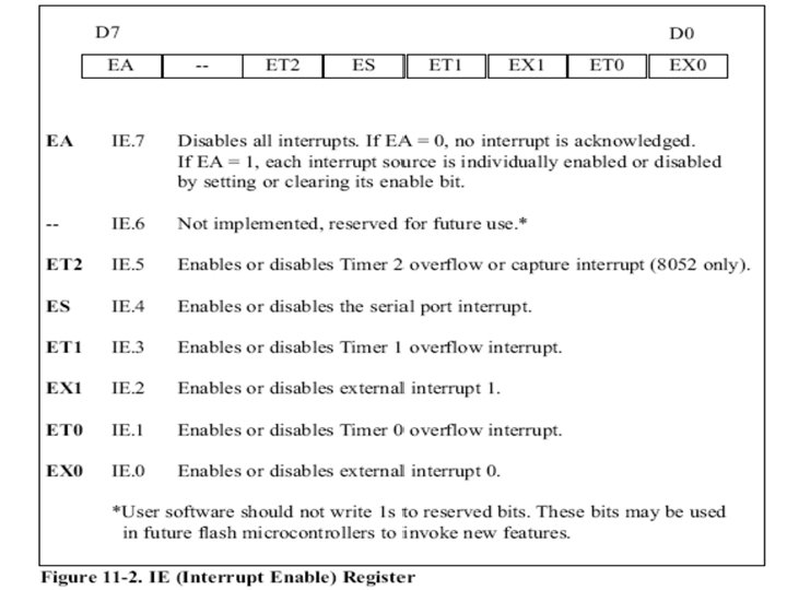
Enabling and Disabling an Interrupt • Upon reset, all interrupts are disabled (masked) None will be responded to by the microcontroller if they are activated • The interrupts must be enabled by software in order for the microcontroller to respond to them • There is a register called IE (interrupt enable) that is responsible for enabling (unmasking) and disabling (masking) the interrupts