Lecture Set 3 Architecture of the 8051 Microcontroller
- Slides: 40

Lecture Set 3 Architecture of the 8051 Microcontroller Universiti Malaysia Perlis Uni. MAP 1

The MCS-51 Family of Microcontrollers • Originally introduced by Intel in 1981. – Currently, the most widely used microcontroller. – 8 -bit processor. – 2 distinct separately addressable memory areas. • Maximum of 64 K on-chip ROM. – Usually 0 to 4 K. • Maximum of 64 K external data memory. • Maximum of 64 K external code memory. • Basic version (8051) contains: – 4 K Bytes of on-chip ROM instruction memory. – 128 Bytes of on-chip RAM for temporary data storage and the stack. – 2 timers, one serial port, and four 8 -bit parallel I/O ports. – Speeds starting from 12 MHz. Universiti Malaysia Perlis Uni. MAP 2

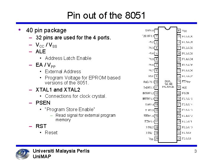
Pin out of the 8051 • 40 pin package – 32 pins are used for the 4 ports. – VCC / VSS – ALE • Address Latch Enable – EA / VPP • External Address • Program Voltage for EPROM based versions of the 8051. – XTAL 1 and XTAL 2 • Connections for clock crystal. – PSEN • “Program Store Enable” – Read signal for external program memory – RST • Reset Universiti Malaysia Perlis Uni. MAP 3

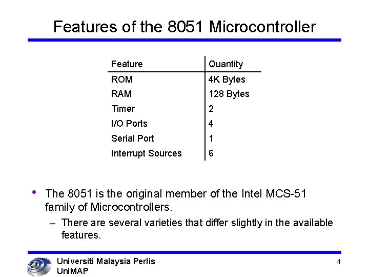
Features of the 8051 Microcontroller • Feature Quantity ROM 4 K Bytes RAM 128 Bytes Timer 2 I/O Ports 4 Serial Port 1 Interrupt Sources 6 The 8051 is the original member of the Intel MCS-51 family of Microcontrollers. – There are several varieties that differ slightly in the available features. Universiti Malaysia Perlis Uni. MAP 4

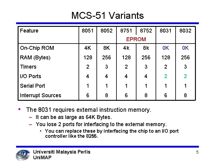
MCS-51 Variants Feature 8051 8052 8751 8752 8031 8032 EPROM On-Chip ROM 4 K 8 K 4 k 8 k 0 K 0 K RAM (Bytes) 128 256 Timers 2 3 2 3 I/O Ports 4 4 2 2 Serial Port 1 1 1 Interrupt Sources 6 8 6 8 • The 8031 requires external instruction memory. – It can be as large as 64 K Bytes. – You lose 2 ports for interfacing to the external memory. • You can replace these by interfacing the chip to an I/O port controller like the 8255. Universiti Malaysia Perlis Uni. MAP 5

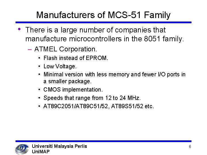
Manufacturers of MCS-51 Family • There is a large number of companies that manufacture microcontrollers in the 8051 family. – ATMEL Corporation. • Flash instead of EPROM. • Low Voltage. • Minimal version with less memory and fewer I/O ports in a smaller package. • CMOS implementation. • Speeds that range from 12 to 24 MHz. • AT 89 C 2051/AT 89 C 51/52, AT 89 S 51/52 etc. Universiti Malaysia Perlis Uni. MAP 6

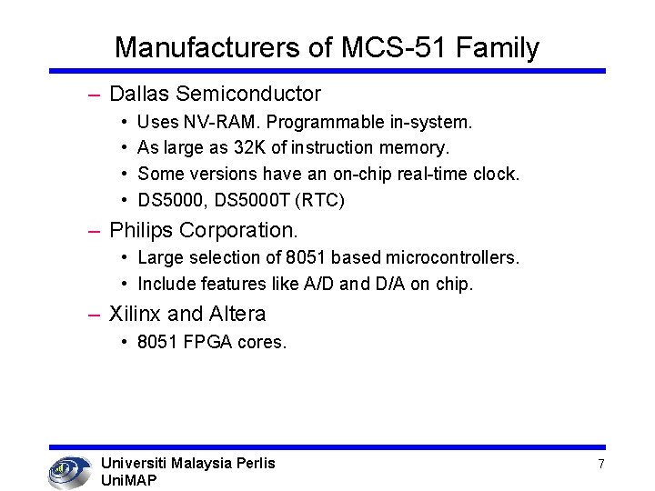
Manufacturers of MCS-51 Family – Dallas Semiconductor • • Uses NV-RAM. Programmable in-system. As large as 32 K of instruction memory. Some versions have an on-chip real-time clock. DS 5000, DS 5000 T (RTC) – Philips Corporation. • Large selection of 8051 based microcontrollers. • Include features like A/D and D/A on chip. – Xilinx and Altera • 8051 FPGA cores. Universiti Malaysia Perlis Uni. MAP 7

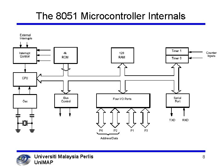
The 8051 Microcontroller Internals Universiti Malaysia Perlis Uni. MAP 8

8051 Architecture • Programmer’s View – Memory Organization – Register Set – Instruction Set • Hardware Designer’s View – Pin-out – Timing characteristics – Current / Voltage requirements Universiti Malaysia Perlis Uni. MAP 9

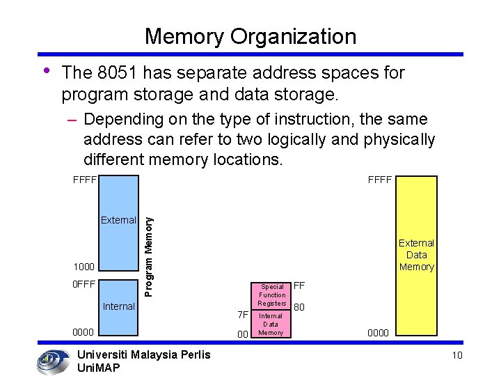
Memory Organization The 8051 has separate address spaces for program storage and data storage. – Depending on the type of instruction, the same address can refer to two logically and physically different memory locations. FFFF External 1000 0 FFF Program Memory • Internal 0000 Universiti Malaysia Perlis Uni. MAP External Data Memory Special Function Registers 7 F 00 Internal Data Memory FF 80 0000 10

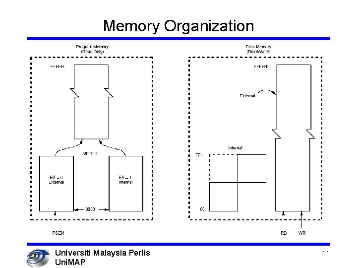
Memory Organization Universiti Malaysia Perlis Uni. MAP 11

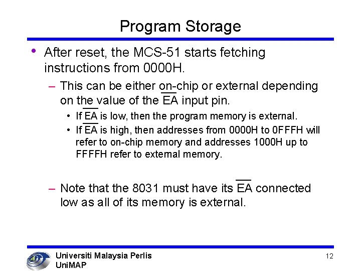
Program Storage • After reset, the MCS-51 starts fetching instructions from 0000 H. – This can be either on-chip or external depending on the value of the EA input pin. • If EA is low, then the program memory is external. • If EA is high, then addresses from 0000 H to 0 FFFH will refer to on-chip memory and addresses 1000 H up to FFFFH refer to external memory. – Note that the 8031 must have its EA connected low as all of its memory is external. Universiti Malaysia Perlis Uni. MAP 12

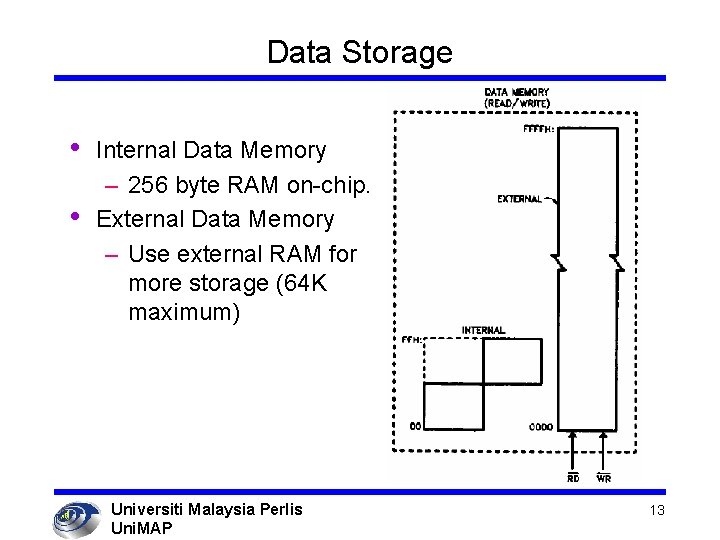
Data Storage • • Internal Data Memory – 256 byte RAM on-chip. External Data Memory – Use external RAM for more storage (64 K maximum) Universiti Malaysia Perlis Uni. MAP 13

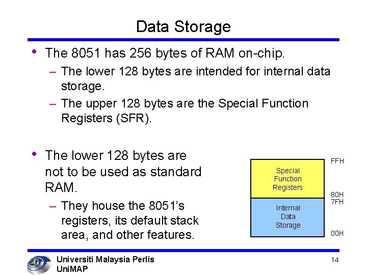
Data Storage • The 8051 has 256 bytes of RAM on-chip. – The lower 128 bytes are intended for internal data storage. – The upper 128 bytes are the Special Function Registers (SFR). • The lower 128 bytes are not to be used as standard RAM. – They house the 8051’s registers, its default stack area, and other features. Universiti Malaysia Perlis Uni. MAP FFH Special Function Registers Internal Data Storage 80 H 7 FH 00 H 14

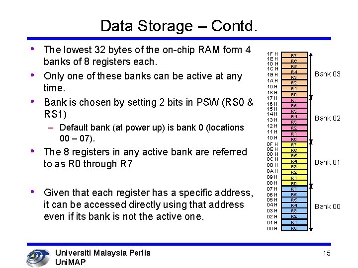
Data Storage – Contd. • • • The lowest 32 bytes of the on-chip RAM form 4 banks of 8 registers each. Only one of these banks can be active at any time. Bank is chosen by setting 2 bits in PSW (RS 0 & RS 1) – Default bank (at power up) is bank 0 (locations 00 – 07). • • The 8 registers in any active bank are referred to as R 0 through R 7 Given that each register has a specific address, it can be accessed directly using that address even if its bank is not the active one. Universiti Malaysia Perlis Uni. MAP 1 F H 1 E H 1 D H 1 C H 1 B H 1 A H 19 H 18 H 17 H 16 H 15 H 14 H 13 H 12 H 11 H 10 H 0 F H 0 E H 0 D H 0 C H 0 B H 0 A H 09 H 08 H 07 H 06 H 05 H 04 H 03 H 02 H 01 H 00 H R 7 R 6 R 5 R 4 R 3 R 2 R 1 R 0 Bank 03 Bank 02 Bank 01 Bank 00 15

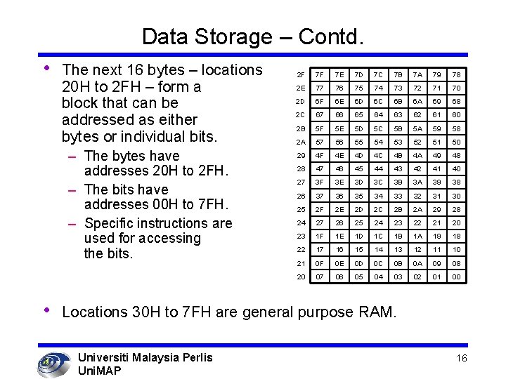
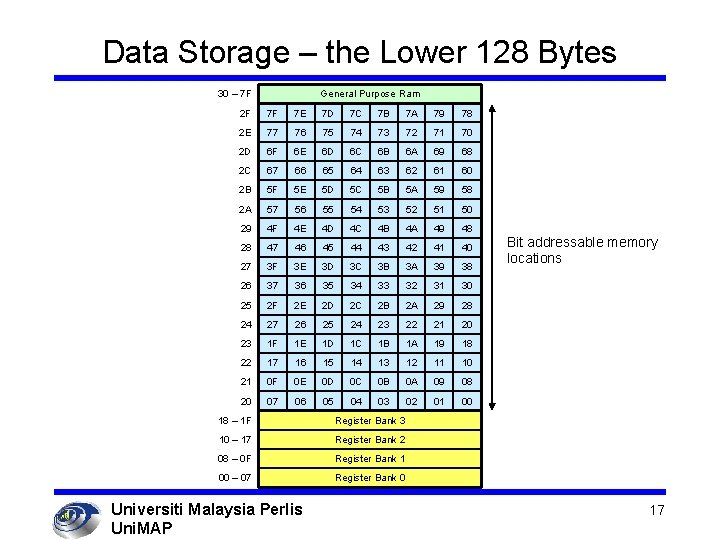
Data Storage – Contd. • The next 16 bytes – locations 20 H to 2 FH – form a block that can be addressed as either bytes or individual bits. – The bytes have addresses 20 H to 2 FH. – The bits have addresses 00 H to 7 FH. – Specific instructions are used for accessing the bits. • 2 F 7 F 7 E 7 D 7 C 7 B 7 A 79 78 2 E 77 76 75 74 73 72 71 70 2 D 6 F 6 E 6 D 6 C 6 B 6 A 69 68 2 C 67 66 65 64 63 62 61 60 2 B 5 F 5 E 5 D 5 C 5 B 5 A 59 58 2 A 57 56 55 54 53 52 51 50 29 4 F 4 E 4 D 4 C 4 B 4 A 49 48 28 47 46 45 44 43 42 41 40 27 3 F 3 E 3 D 3 C 3 B 3 A 39 38 26 37 36 35 34 33 32 31 30 25 2 F 2 E 2 D 2 C 2 B 2 A 29 28 24 27 26 25 24 23 22 21 20 23 1 F 1 E 1 D 1 C 1 B 1 A 19 18 22 17 16 15 14 13 12 11 10 21 0 F 0 E 0 D 0 C 0 B 0 A 09 08 20 07 06 05 04 03 02 01 00 Locations 30 H to 7 FH are general purpose RAM. Universiti Malaysia Perlis Uni. MAP 16

Data Storage – the Lower 128 Bytes 30 – 7 F General Purpose Ram 2 F 7 F 7 E 7 D 7 C 7 B 7 A 79 78 2 E 77 76 75 74 73 72 71 70 2 D 6 F 6 E 6 D 6 C 6 B 6 A 69 68 2 C 67 66 65 64 63 62 61 60 2 B 5 F 5 E 5 D 5 C 5 B 5 A 59 58 2 A 57 56 55 54 53 52 51 50 29 4 F 4 E 4 D 4 C 4 B 4 A 49 48 28 47 46 45 44 43 42 41 40 27 3 F 3 E 3 D 3 C 3 B 3 A 39 38 26 37 36 35 34 33 32 31 30 25 2 F 2 E 2 D 2 C 2 B 2 A 29 28 24 27 26 25 24 23 22 21 20 23 1 F 1 E 1 D 1 C 1 B 1 A 19 18 22 17 16 15 14 13 12 11 10 21 0 F 0 E 0 D 0 C 0 B 0 A 09 08 20 07 06 05 04 03 02 01 00 18 – 1 F Register Bank 3 10 – 17 Register Bank 2 08 – 0 F Register Bank 1 00 – 07 Register Bank 0 Universiti Malaysia Perlis Uni. MAP Bit addressable memory locations 17

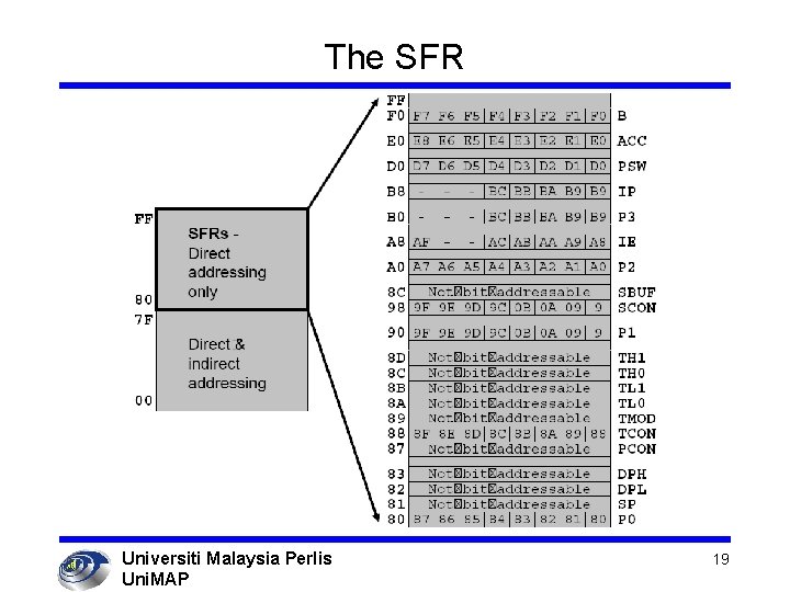
The SFR – Special Function Registers • The upper 128 bytes of the on-chip RAM are used to house special function registers. • In reality, only about 25 of these bytes are actually used. The others are reserved for future versions of the 8051. – These are registers associated with important functions in the operation of the MCS-51. – Some of these registers are bit-addressable as well as byte-addressable. • The address of bit 0 of the register will be the same as the address of the register. Universiti Malaysia Perlis Uni. MAP 18

The SFR Universiti Malaysia Perlis Uni. MAP 19

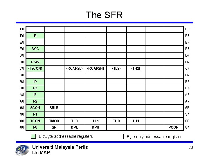
The SFR F 8 F 0 FF B F 7 E 8 E 0 EF ACC E 7 D 8 DF D 0 PSW C 8 (T 2 CON) D 7 (RCAP 2 L) (RCAP 2 H) (TL 2) (TH 2) CF C 0 C 7 B 8 IP BF B 0 P 3 B 7 A 8 IE AF A 0 P 2 A 7 98 SCON 90 P 1 88 TCON TMOD TL 0 TL 1 80 P 0 SP DPL DPH SBUF 9 F 97 Bit/Byte addressable registers Universiti Malaysia Perlis Uni. MAP TH 0 TH 1 8 F PCON 87 Byte only addressable registers 20

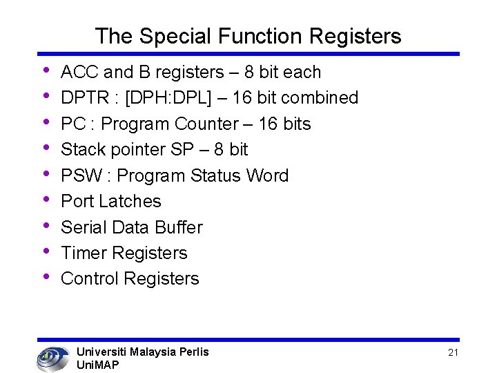
The Special Function Registers • • • ACC and B registers – 8 bit each DPTR : [DPH: DPL] – 16 bit combined PC : Program Counter – 16 bits Stack pointer SP – 8 bit PSW : Program Status Word Port Latches Serial Data Buffer Timer Registers Control Registers Universiti Malaysia Perlis Uni. MAP 21

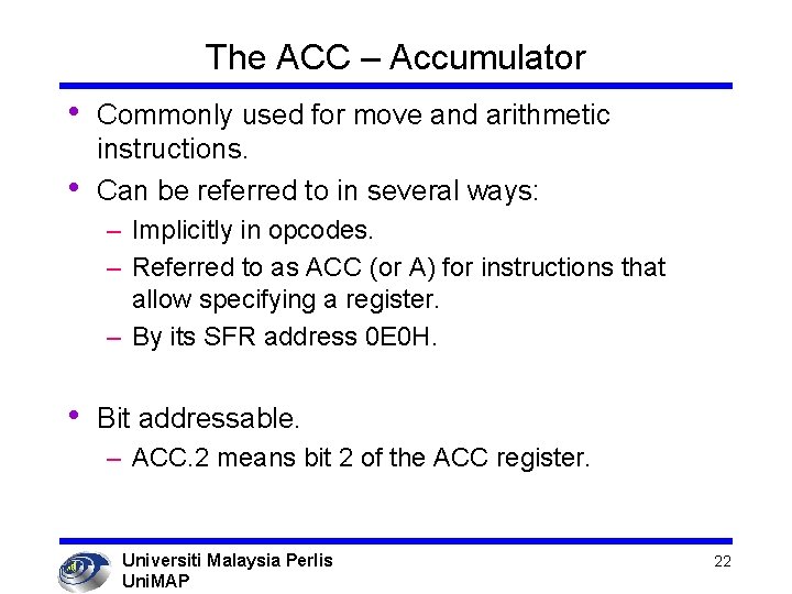
The ACC – Accumulator • • Commonly used for move and arithmetic instructions. Can be referred to in several ways: – Implicitly in opcodes. – Referred to as ACC (or A) for instructions that allow specifying a register. – By its SFR address 0 E 0 H. • Bit addressable. – ACC. 2 means bit 2 of the ACC register. Universiti Malaysia Perlis Uni. MAP 22

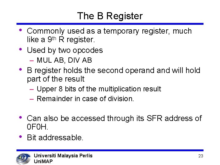
The B Register • • • Commonly used as a temporary register, much like a 9 th R register. Used by two opcodes – MUL AB, DIV AB B register holds the second operand will hold part of the result – Upper 8 bits of the multiplication result – Remainder in case of division. • • Can also be accessed through its SFR address of 0 F 0 H. Bit addressable. Universiti Malaysia Perlis Uni. MAP 23

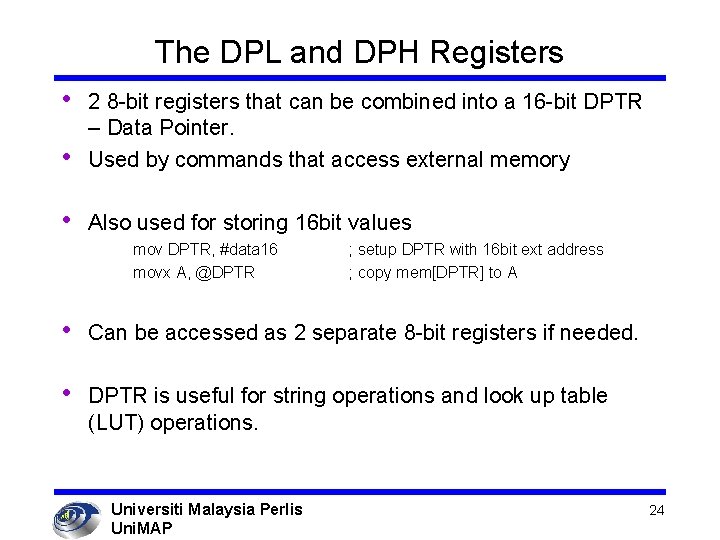
The DPL and DPH Registers • • 2 8 -bit registers that can be combined into a 16 -bit DPTR – Data Pointer. Used by commands that access external memory • Also used for storing 16 bit values mov DPTR, #data 16 movx A, @DPTR ; setup DPTR with 16 bit ext address ; copy mem[DPTR] to A • Can be accessed as 2 separate 8 -bit registers if needed. • DPTR is useful for string operations and look up table (LUT) operations. Universiti Malaysia Perlis Uni. MAP 24

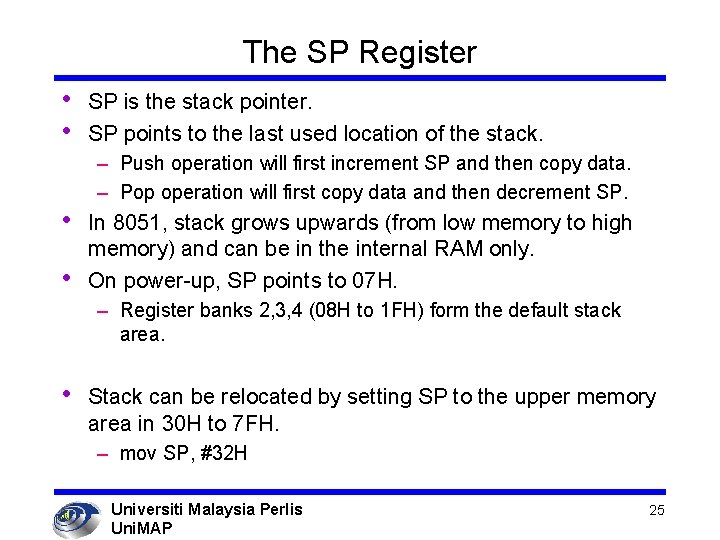
The SP Register • • SP is the stack pointer. SP points to the last used location of the stack. – Push operation will first increment SP and then copy data. – Pop operation will first copy data and then decrement SP. • • In 8051, stack grows upwards (from low memory to high memory) and can be in the internal RAM only. On power-up, SP points to 07 H. – Register banks 2, 3, 4 (08 H to 1 FH) form the default stack area. • Stack can be relocated by setting SP to the upper memory area in 30 H to 7 FH. – mov SP, #32 H Universiti Malaysia Perlis Uni. MAP 25

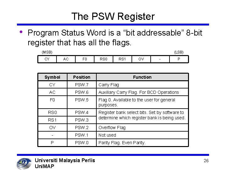
The PSW Register • Program Status Word is a “bit addressable” 8 -bit register that has all the flags. (MSB) CY (LSB) AC F 0 RS 1 OV - P Symbol Position CY PSW. 7 Carry Flag AC PSW. 6 Auxiliary Carry Flag. For BCD Operations F 0 PSW. 5 Flag 0. Available to the user for general purposes. RS 0 PSW. 4 RS 1 PSW. 3 Register bank select bits. Set by software to determine which register bank is being used. OV PSW. 2 Overflow Flag - PSW. 1 Not used P PSW. 0 Parity Flag. Even Parity. Universiti Malaysia Perlis Uni. MAP Function 26

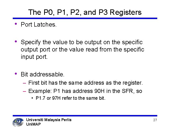
The P 0, P 1, P 2, and P 3 Registers • Port Latches. • Specify the value to be output on the specific output port or the value read from the specific input port. • Bit addressable. – First bit has the same address as the register. – Example: P 1 has address 90 H in the SFR, so • P 1. 7 or 97 H refer to the same bit. Universiti Malaysia Perlis Uni. MAP 27

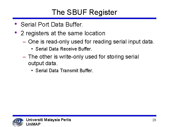
The SBUF Register • • Serial Port Data Buffer. 2 registers at the same location – One is read-only used for reading serial input data. • Serial Data Receive Buffer. – The other is write-only used for storing serial output data. • Serial Data Transmit Buffer. Universiti Malaysia Perlis Uni. MAP 28

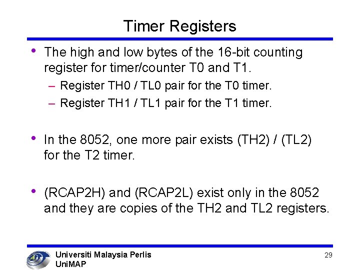
Timer Registers • The high and low bytes of the 16 -bit counting register for timer/counter T 0 and T 1. – Register TH 0 / TL 0 pair for the T 0 timer. – Register TH 1 / TL 1 pair for the T 1 timer. • In the 8052, one more pair exists (TH 2) / (TL 2) for the T 2 timer. • (RCAP 2 H) and (RCAP 2 L) exist only in the 8052 and they are copies of the TH 2 and TL 2 registers. Universiti Malaysia Perlis Uni. MAP 29

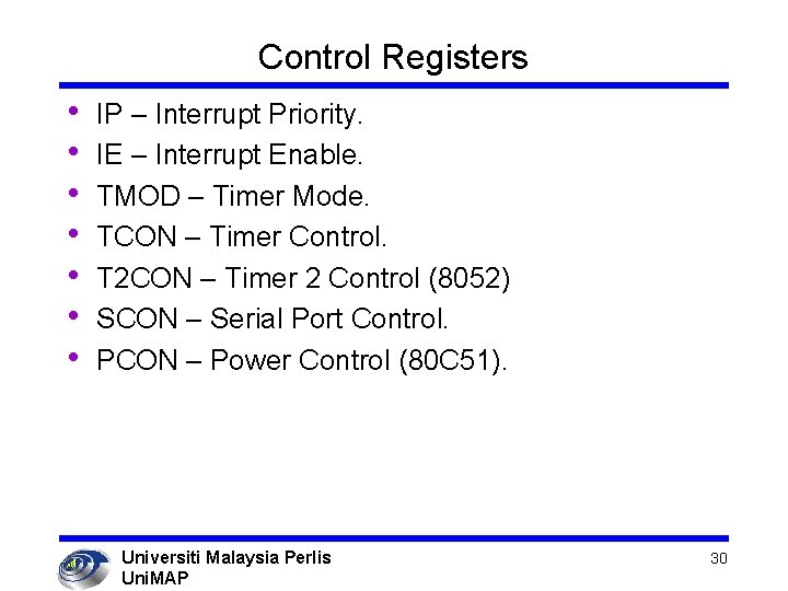
Control Registers • • IP – Interrupt Priority. IE – Interrupt Enable. TMOD – Timer Mode. TCON – Timer Control. T 2 CON – Timer 2 Control (8052) SCON – Serial Port Control. PCON – Power Control (80 C 51). Universiti Malaysia Perlis Uni. MAP 30

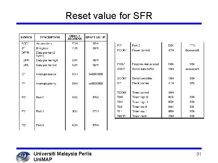
Reset value for SFR Universiti Malaysia Perlis Uni. MAP 31

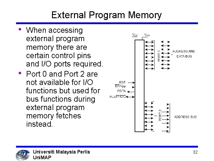
External Program Memory • • When accessing external program memory there are certain control pins and I/O ports required. Port 0 and Port 2 are not available for I/O functions but used for bus functions during external program memory fetches instead. Universiti Malaysia Perlis Uni. MAP 32

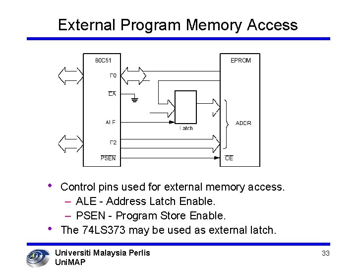
External Program Memory Access • • Control pins used for external memory access. – ALE - Address Latch Enable. – PSEN - Program Store Enable. The 74 LS 373 may be used as external latch. Universiti Malaysia Perlis Uni. MAP 33

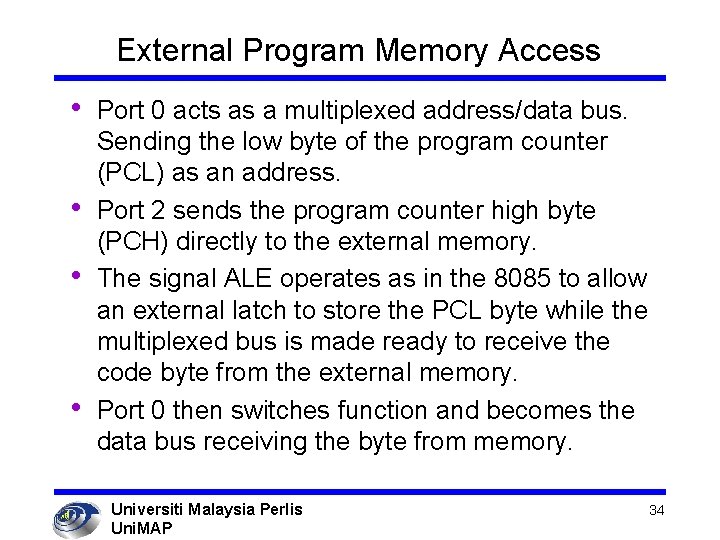
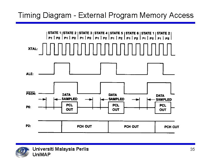
External Program Memory Access • • Port 0 acts as a multiplexed address/data bus. Sending the low byte of the program counter (PCL) as an address. Port 2 sends the program counter high byte (PCH) directly to the external memory. The signal ALE operates as in the 8085 to allow an external latch to store the PCL byte while the multiplexed bus is made ready to receive the code byte from the external memory. Port 0 then switches function and becomes the data bus receiving the byte from memory. Universiti Malaysia Perlis Uni. MAP 34

Timing Diagram - External Program Memory Access Universiti Malaysia Perlis Uni. MAP 35

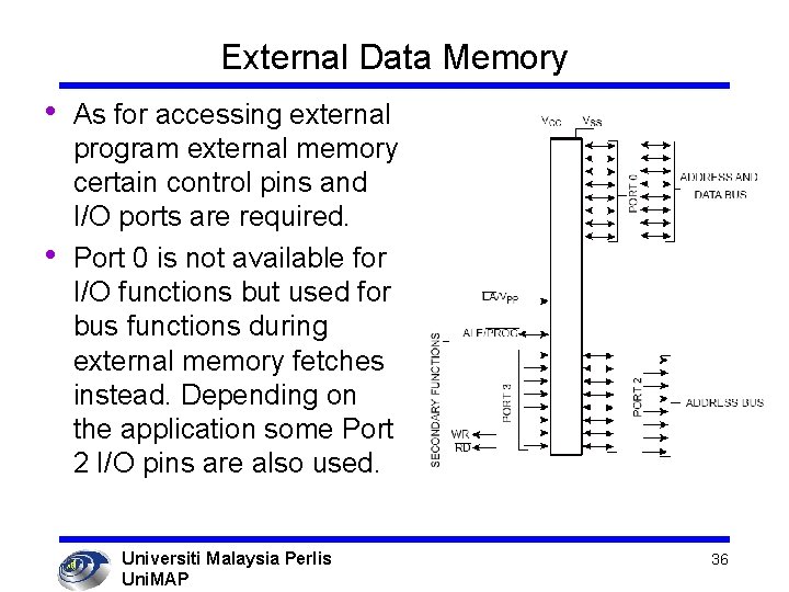
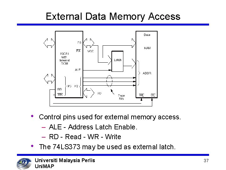
External Data Memory • • As for accessing external program external memory certain control pins and I/O ports are required. Port 0 is not available for I/O functions but used for bus functions during external memory fetches instead. Depending on the application some Port 2 I/O pins are also used. Universiti Malaysia Perlis Uni. MAP 36

External Data Memory Access • • Control pins used for external memory access. – ALE - Address Latch Enable. – RD - Read - WR - Write The 74 LS 373 may be used as external latch. Universiti Malaysia Perlis Uni. MAP 37

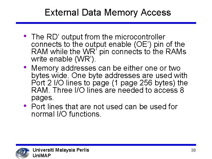
External Data Memory Access • • • The RD’ output from the microcontroller connects to the output enable (OE’) pin of the RAM while the WR’ pin connects to the RAMs write enable (WR’). Memory addresses can be either one or two bytes wide. One byte addresses are used with Port 2 I/O lines to page (1 page 256 bytes) the RAM. Three I/O lines are needed to access 8 pages. Port lines that are not used can be used for normal I/O functions. Universiti Malaysia Perlis Uni. MAP 38

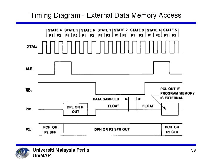
Timing Diagram - External Data Memory Access Universiti Malaysia Perlis Uni. MAP 39

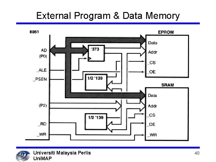
External Program & Data Memory Universiti Malaysia Perlis Uni. MAP 40