Unit IV PIC Microcontroller Architecture PIC Microcontroller PIC
- Slides: 93

Unit IV PIC Microcontroller Architecture

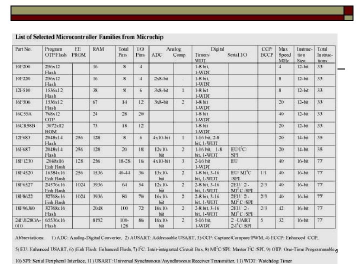
PIC Microcontroller PIC 16 CXX, PIC 18 FXX are 8 -bit microcontroller by Microchip. It uses High speed RISC Architecture PIC are popular due to High performance, Low cost, & small Size. Mostly Single word instructions, except 4 two word instructions. Operating frequency for 18 CXX – DC to 40 MHz Some advanced versions include ADC with 4 -8 Channels General features includes Timers, Watch dog timers, ADC, Extended Instruction / Data memory, Serial communication , Capture/ Compare/ Pulse width modulation (CCP).

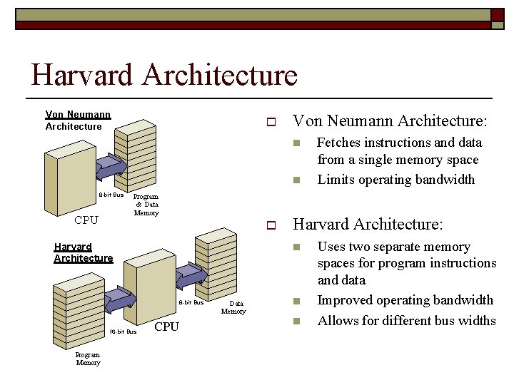
Harvard Architecture Von Neumann Architecture: 8 -bit Bus CPU Program & Data Memory 8 -bit Bus 16 -bit Bus Program Memory Harvard Architecture: Harvard Architecture CPU Data Memory Fetches instructions and data from a single memory space Limits operating bandwidth Uses two separate memory spaces for program instructions and data Improved operating bandwidth Allows for different bus widths

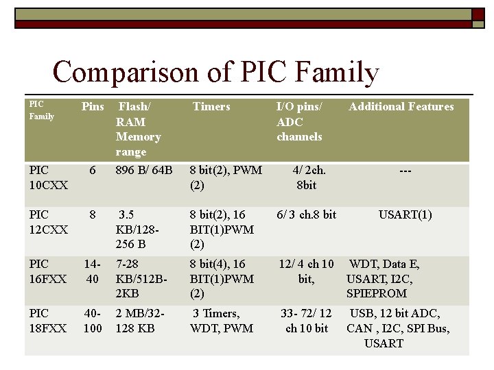
Comparison of PIC Family Pins Flash/ RAM Memory range Timers PIC 10 CXX 6 896 B/ 64 B 8 bit(2), PWM (2) PIC 12 CXX 8 3. 5 KB/128256 B PIC 16 FXX 1440 PIC 18 FXX 40100 I/O pins/ ADC channels Additional Features 4/ 2 ch. 8 bit --- 8 bit(2), 16 BIT(1)PWM (2) 6/ 3 ch. 8 bit USART(1) 7 -28 KB/512 B 2 KB 8 bit(4), 16 BIT(1)PWM (2) 12/ 4 ch 10 WDT, Data E, bit, USART, I 2 C, SPIEPROM 2 MB/32128 KB 3 Timers, WDT, PWM 33 - 72/ 12 ch 10 bit USB, 12 bit ADC, CAN , I 2 C, SPI Bus, USART

5

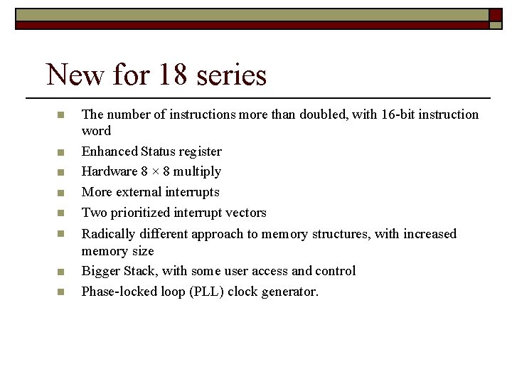
New for 18 series The number of instructions more than doubled, with 16 -bit instruction word Enhanced Status register Hardware 8 × 8 multiply More external interrupts Two prioritized interrupt vectors Radically different approach to memory structures, with increased memory size Bigger Stack, with some user access and control Phase-locked loop (PLL) clock generator.

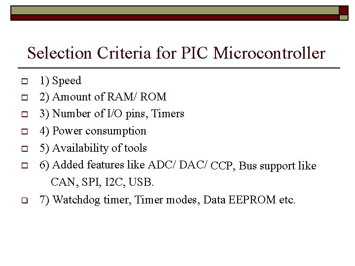
Selection Criteria for PIC Microcontroller 1) Speed 2) Amount of RAM/ ROM 3) Number of I/O pins, Timers 4) Power consumption 5) Availability of tools 6) Added features like ADC/ DAC/ CCP, Bus support like CAN, SPI, I 2 C, USB. 7) Watchdog timer, Timer modes, Data EEPROM etc.

PIC 18 F 458 High-Performance, Enhanced Flash Microcontrollers with CAN

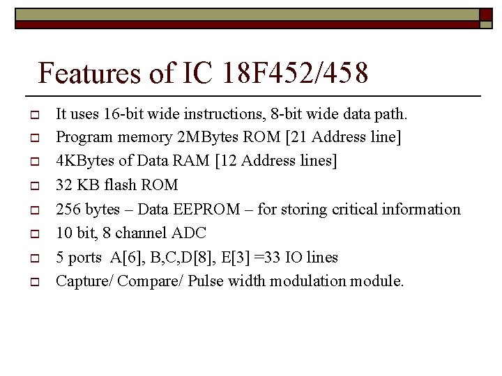
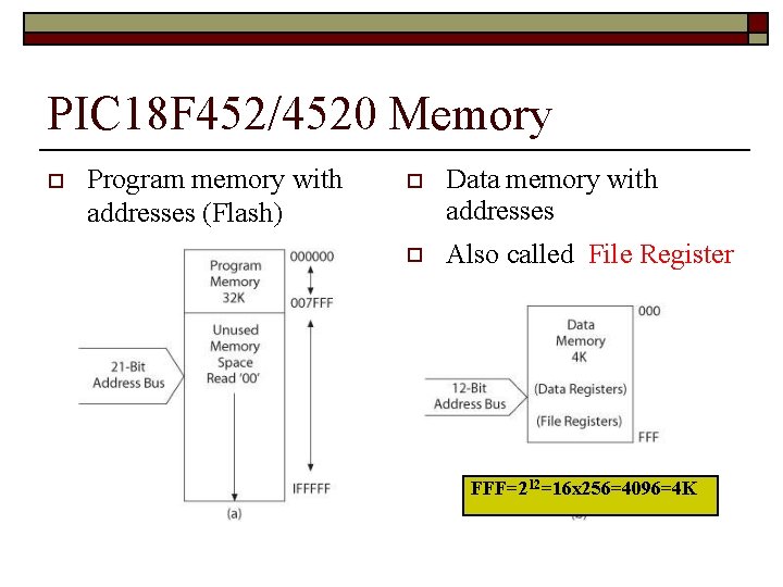
Features of IC 18 F 452/458 It uses 16 -bit wide instructions, 8 -bit wide data path. Program memory 2 MBytes ROM [21 Address line] 4 KBytes of Data RAM [12 Address lines] 32 KB flash ROM 256 bytes – Data EEPROM – for storing critical information 10 bit, 8 channel ADC 5 ports A[6], B, C, D[8], E[3] =33 IO lines Capture/ Compare/ Pulse width modulation module.

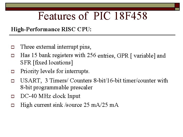
Features of PIC 18 F 458 High-Performance RISC CPU: Three external interrupt pins, Has 15 bank registers with 256 entries, GPR [ variable] and SFR [fixed locations] Priority levels for interrupts. USART, 3 Timers/ Counters 8 -bit/16 -bit timer/counter with 8 -bit programmable prescaler DC-40 MHz clock Input High current sink /source 25 m. A/25 m. A

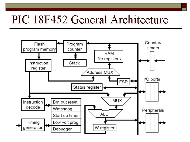
PIC 18 F 452 General Architecture

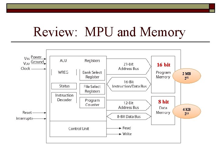
Review: MPU and Memory 16 bit 2 MB 221 8 bit 4 KB 212

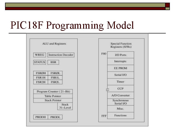
PIC 18 F Programming Model The representation of the internal architecture of a microprocessor, necessary to write assembly language programs Divided into two groups Arithmetic Logic Unit (ALU) and Registers From Microprocessor Unit (MPU) Special Function Registers (SFRs) From Data (File) Memory

PIC 18 F Programming Model 14

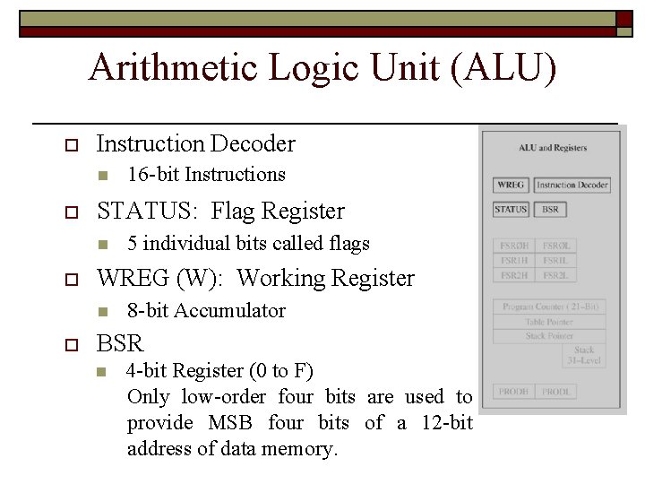
Arithmetic Logic Unit (ALU) Instruction Decoder STATUS: Flag Register 5 individual bits called flags WREG (W): Working Register 16 -bit Instructions 8 -bit Accumulator BSR 4 -bit Register (0 to F) Only low-order four bits are used to provide MSB four bits of a 12 -bit address of data memory.

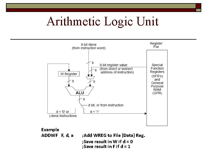
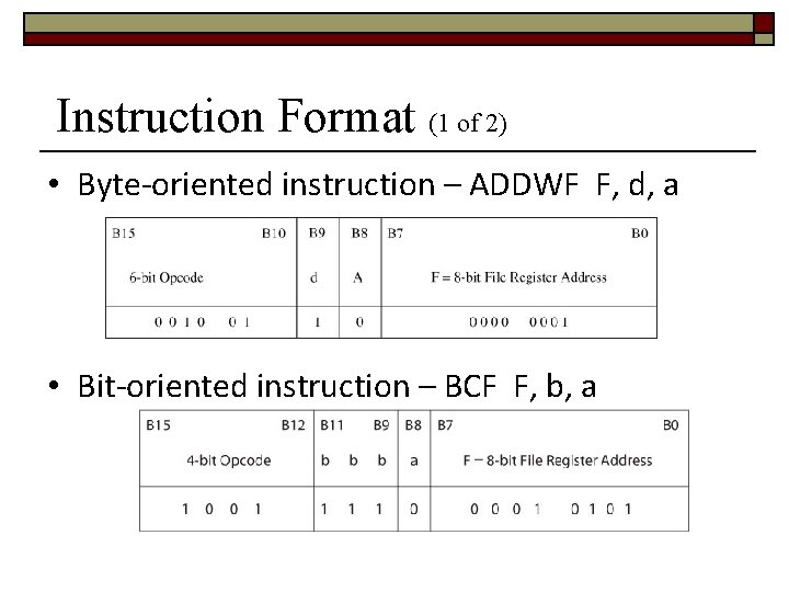
Arithmetic Logic Unit Example ADDWF F, d, a ; Add WREG to File (Data) Reg. ; Save result in W if d = 0 ; Save result in F if d = 1

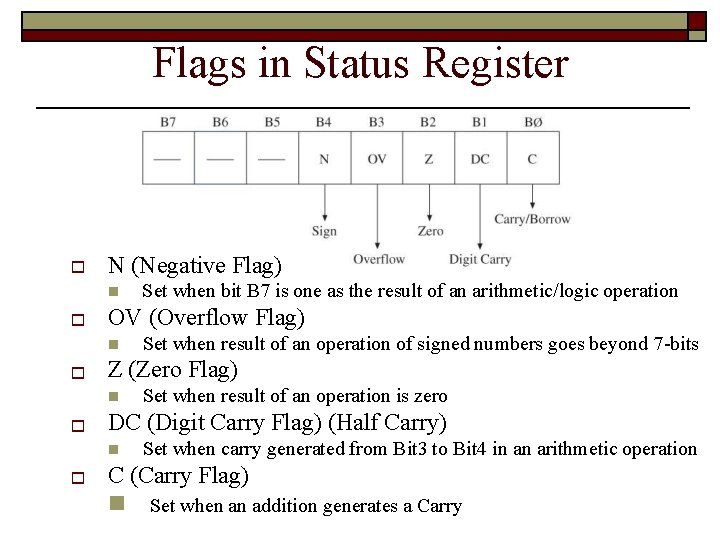
Flags in Status Register N (Negative Flag) OV (Overflow Flag) Set when result of an operation is zero DC (Digit Carry Flag) (Half Carry) Set when result of an operation of signed numbers goes beyond 7 -bits Z (Zero Flag) Set when bit B 7 is one as the result of an arithmetic/logic operation Set when carry generated from Bit 3 to Bit 4 in an arithmetic operation C (Carry Flag) Set when an addition generates a Carry

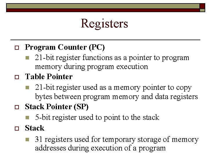
Registers Program Counter (PC) 21 -bit register functions as a pointer to program memory during program execution Table Pointer 21 -bit register used as a memory pointer to copy bytes between program memory and data registers Stack Pointer (SP) 5 -bit register used to point to the stack Stack 31 registers used for temporary storage of memory addresses during execution of a program

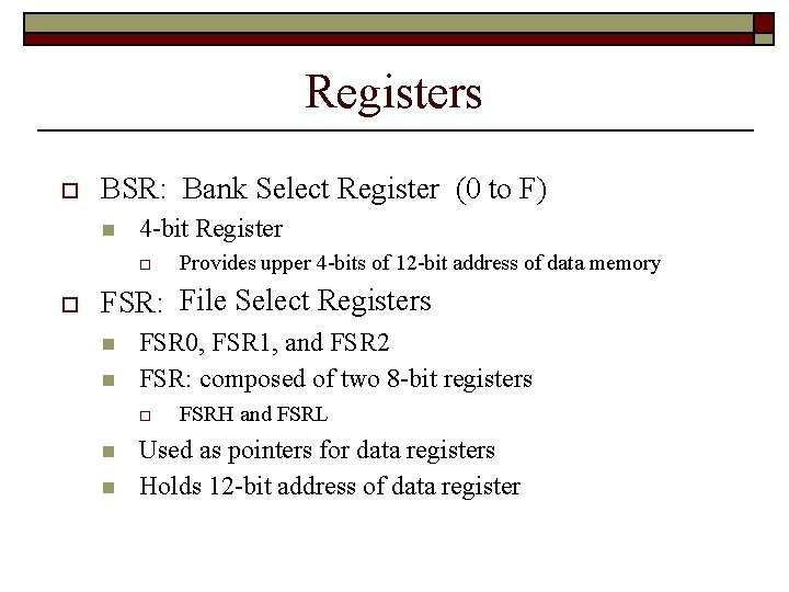
Registers BSR: Bank Select Register (0 to F) 4 -bit Register Provides upper 4 -bits of 12 -bit address of data memory FSR: File Select Registers FSR 0, FSR 1, and FSR 2 FSR: composed of two 8 -bit registers FSRH and FSRL Used as pointers for data registers Holds 12 -bit address of data register

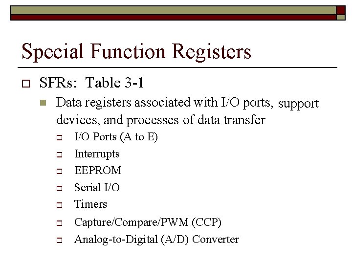
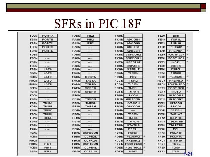
Special Function Registers SFRs: Table 3 -1 Data registers associated with I/O ports, support devices, and processes of data transfer I/O Ports (A to E) Interrupts EEPROM Serial I/O Timers Capture/Compare/PWM (CCP) Analog-to-Digital (A/D) Converter

SFRs in PIC 18 F

PIC 18 F 452/4520 Memory Program memory with addresses (Flash) Data memory with addresses Also called File Register FFF=212=16 x 256=4096=4 K

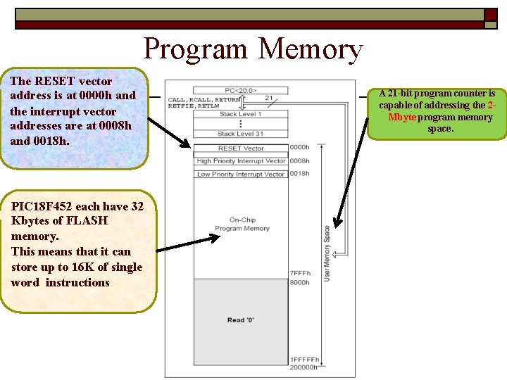
Program Memory The RESET vector address is at 0000 h and the interrupt vector addresses are at 0008 h and 0018 h. PIC 18 F 452 each have 32 Kbytes of FLASH memory. This means that it can store up to 16 K of single word instructions A 21 -bit program counter is capable of addressing the 2 Mbyte program memory space.

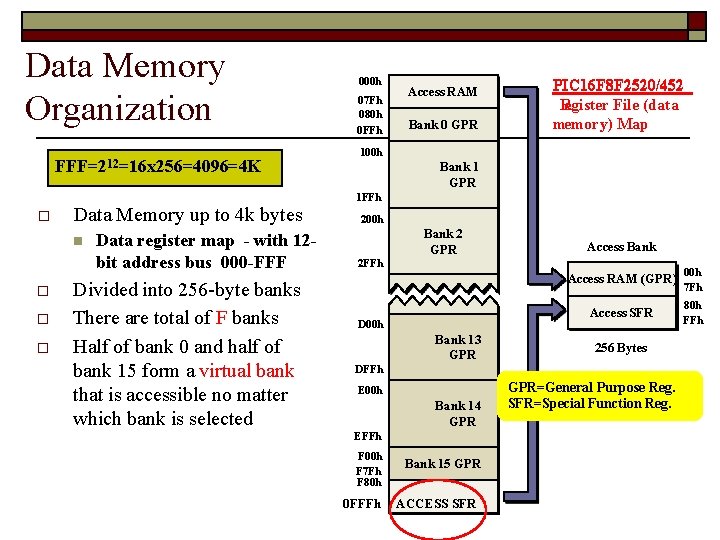
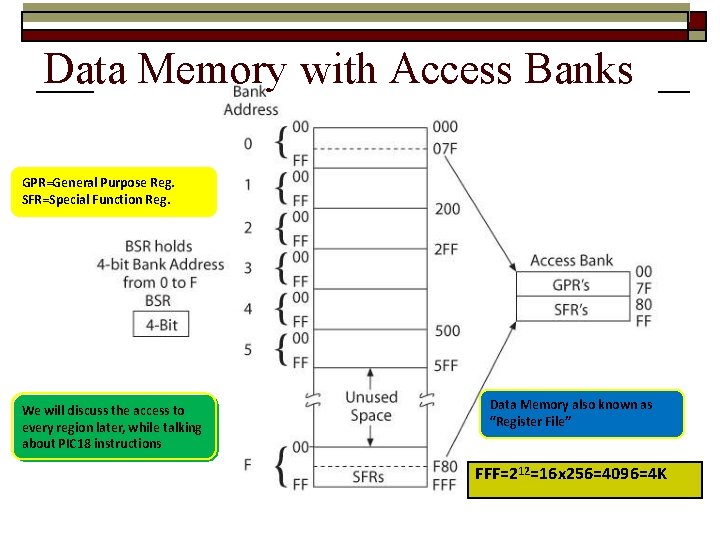
Data Memory Organization FFF=212=16 x 256=4096=4 K 000 h 07 Fh 080 h 0 FFh Access RAM Bank 0 GPR PIC 16 F 8 F 2520/452 Register File (data memory) Map 100 h Bank 1 GPR 1 FFh Data Memory up to 4 k bytes Data register map - with 12 bit address bus 000 -FFF Divided into 256 -byte banks There are total of F banks Half of bank 0 and half of bank 15 form a virtual bank that is accessible no matter which bank is selected 200 h Bank 2 GPR Access Bank 2 FFh D 00 h Bank 13 GPR Access RAM (GPR) 00 h 7 Fh Access SFR 80 h FFh 256 Bytes DFFh E 00 h Bank 14 GPR EFFh F 00 h F 7 Fh F 80 h 0 FFFh Bank 15 GPR ACCESS SFR GPR=General Purpose Reg. SFR=Special Function Reg.

Data Memory with Access Banks GPR=General Purpose Reg. SFR=Special Function Reg. We will discuss the access to every region later, while talking about PIC 18 instructions Data Memory also known as “Register File” FFF=212=16 x 256=4096=4 K

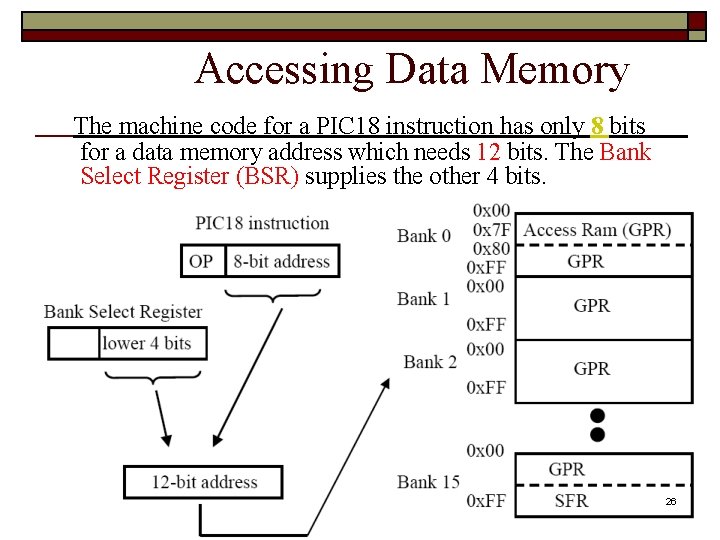
Accessing Data Memory The machine code for a PIC 18 instruction has only 8 bits for a data memory address which needs 12 bits. The Bank Select Register (BSR) supplies the other 4 bits. 26

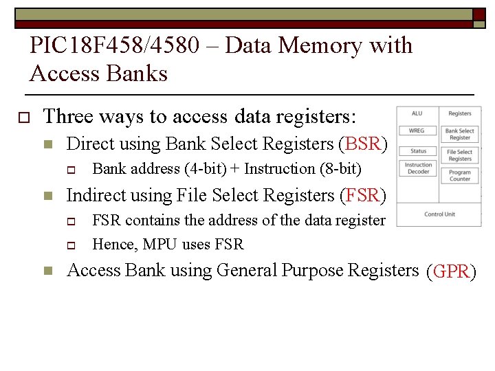
PIC 18 F 458/4580 – Data Memory with Access Banks Three ways to access data registers: Direct using Bank Select Registers (BSR) Indirect using File Select Registers (FSR) Bank address (4 -bit) + Instruction (8 -bit) FSR contains the address of the data register Hence, MPU uses FSR Access Bank using General Purpose Registers (GPR)

Peripherals: Capture- Compare- Pulse Width Modulation ( CCP) The compare mode can cause an event like simply turning on the device when the contents of Timer matches with CCP register. In Capture mode, an event at CCP pin will cause contents of timer to be loaded in CCP register. Pulse width modulation feature allows to create pulses of variable duty cycle. The main difference between Enhanced CCP module and standard CCP is that it allows four pins for implementation of H bridge or half H bridge for DC motor control. - 1, 2 or 4 PWM outputs

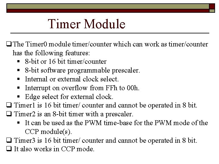
Timer Module The Timer 0 module timer/counter which can work as timer/counter has the following features: § 8 -bit or 16 bit timer/counter § 8 -bit software programmable prescaler. § Internal or external clock select. § Interrupt on overflow from FFh to 00 h. § Edge select for external clock. Timer 1 is 16 bit timer/ counter and cannot be operated in 8 bit. Timer 2 is an 8 -bit timer with a prescaler. § It can be used as the PWM time-base for the PWM mode of the CCP module(s). Timer 3 is 16 bit timer/ counter and cannot be operated in 8 bit. It also works in CCP mode.

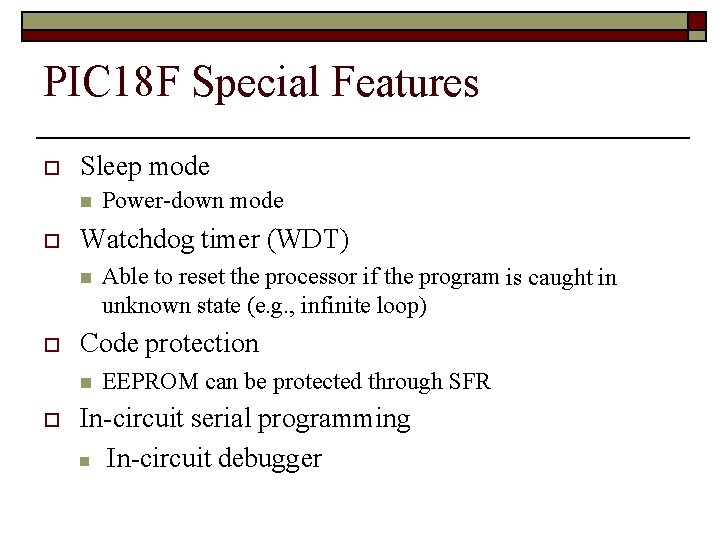
PIC 18 F Special Features Sleep mode Watchdog timer (WDT) Able to reset the processor if the program is caught in unknown state (e. g. , infinite loop) Code protection Power-down mode EEPROM can be protected through SFR In-circuit serial programming In-circuit debugger

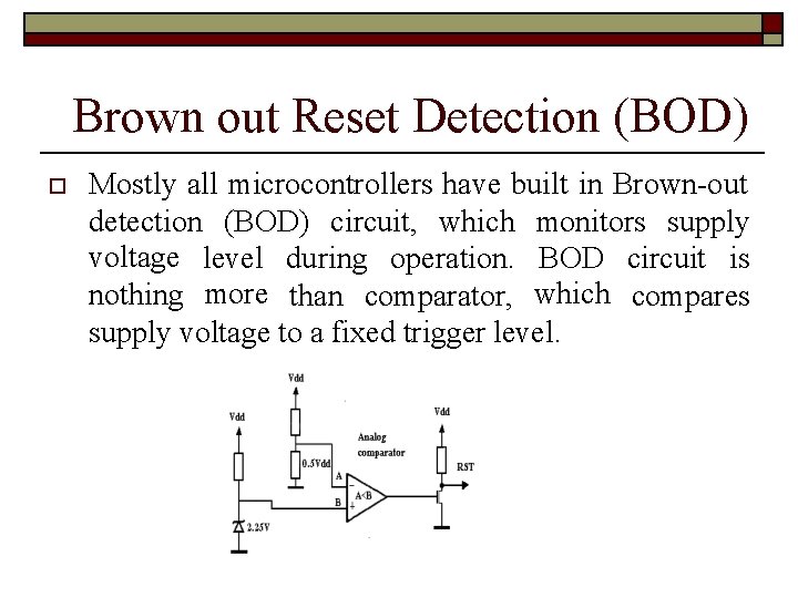
Brown out Reset Detection (BOD) Mostly all microcontrollers have built in Brown-out detection (BOD) circuit, which monitors supply voltage level during operation. BOD circuit is nothing more than comparator, which compares supply voltage to a fixed trigger level.

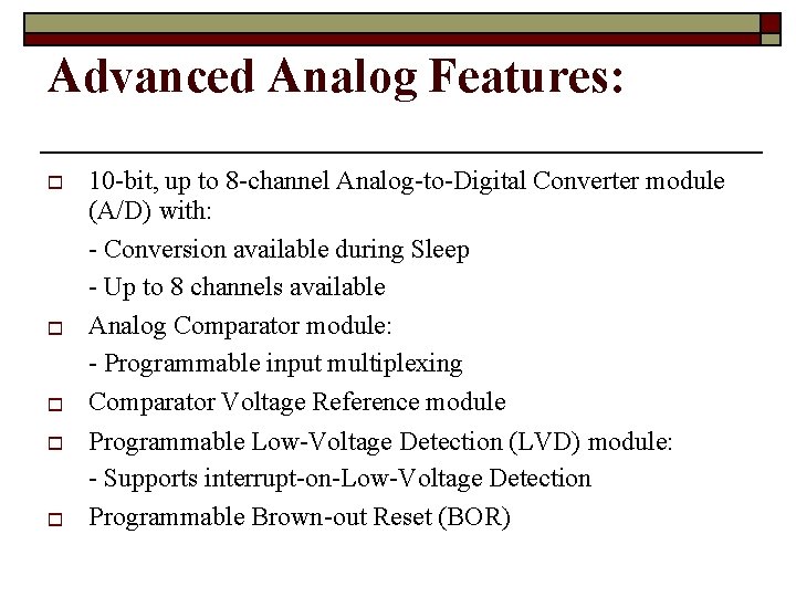
Advanced Analog Features: 10 -bit, up to 8 -channel Analog-to-Digital Converter module (A/D) with: - Conversion available during Sleep - Up to 8 channels available Analog Comparator module: - Programmable input multiplexing Comparator Voltage Reference module Programmable Low-Voltage Detection (LVD) module: - Supports interrupt-on-Low-Voltage Detection Programmable Brown-out Reset (BOR)

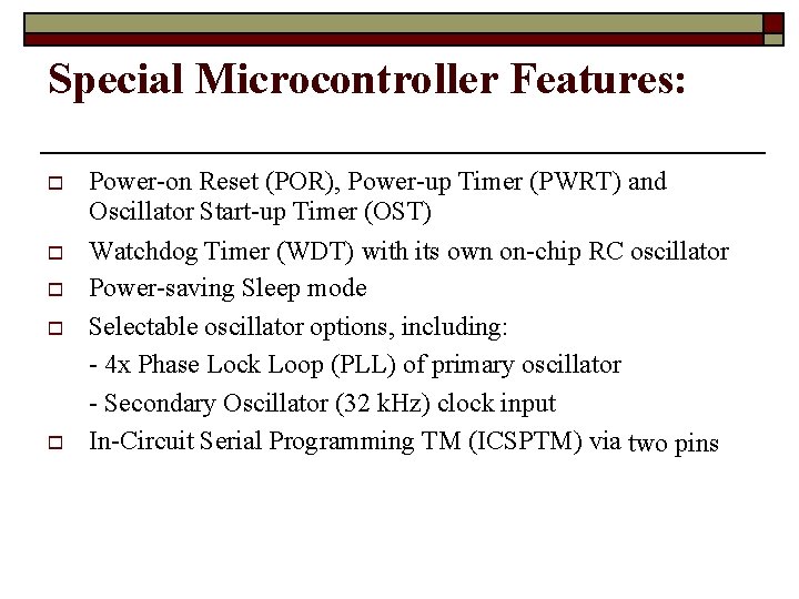
Special Microcontroller Features: Power-on Reset (POR), Power-up Timer (PWRT) and Oscillator Start-up Timer (OST) Watchdog Timer (WDT) with its own on-chip RC oscillator Power-saving Sleep mode Selectable oscillator options, including: - 4 x Phase Lock Loop (PLL) of primary oscillator - Secondary Oscillator (32 k. Hz) clock input In-Circuit Serial Programming TM (ICSPTM) via two pins

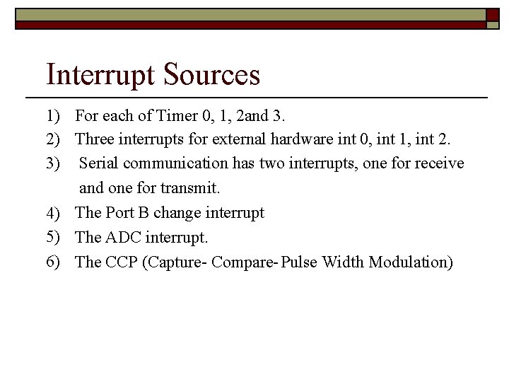
Interrupt Sources 1) For each of Timer 0, 1, 2 and 3. 2) Three interrupts for external hardware int 0, int 1, int 2. 3) Serial communication has two interrupts, one for receive and one for transmit. 4) The Port B change interrupt 5) The ADC interrupt. 6) The CCP (Capture- Compare- Pulse Width Modulation)

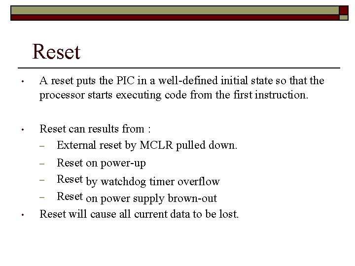
Reset • A reset puts the PIC in a well-defined initial state so that the processor starts executing code from the first instruction. • Reset can results from : – External reset by MCLR pulled down. – – – • Reset on power-up Reset by watchdog timer overflow Reset on power supply brown-out Reset will cause all current data to be lost.

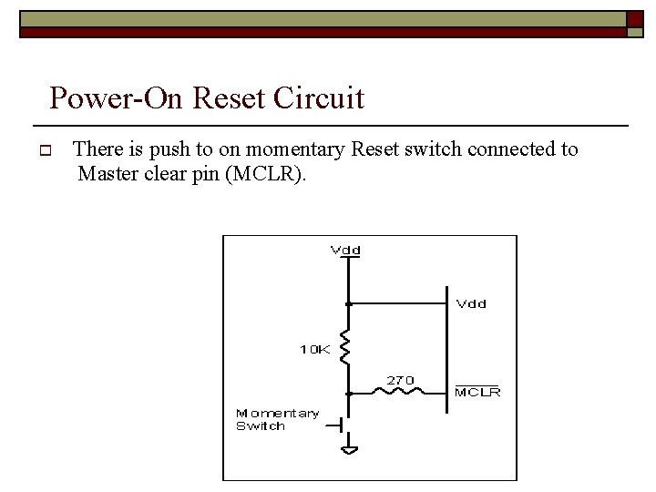
Power-On Reset Circuit There is push to on momentary Reset switch connected to Master clear pin (MCLR).

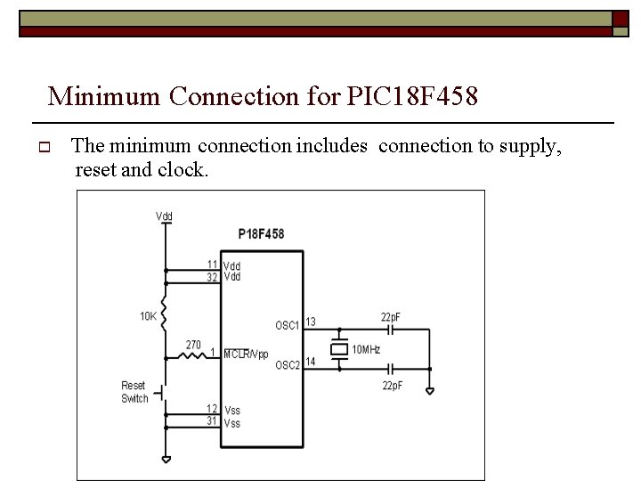
Minimum Connection for PIC 18 F 458 The minimum connection includes connection to supply, reset and clock.

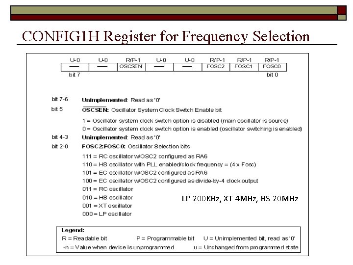
CONFIG 1 H Register for Frequency Selection LP-200 KHz, XT-4 MHz, HS-20 MHz

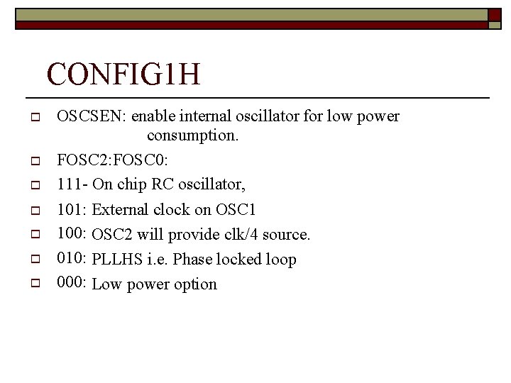
CONFIG 1 H OSCSEN: enable internal oscillator for low power consumption. FOSC 2: FOSC 0: 111 - On chip RC oscillator, 101: External clock on OSC 1 100: OSC 2 will provide clk/4 source. 010: PLLHS i. e. Phase locked loop 000: Low power option

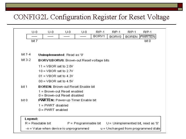
CONFIG 2 L Configuration Register for Reset Voltage

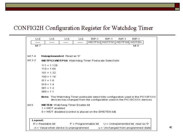
CONFIG 2 H Configuration Register for Watchdog Timer 42

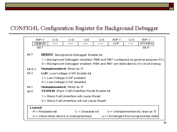
CONFIG 4 L Configuration Register for Background Debugger 43

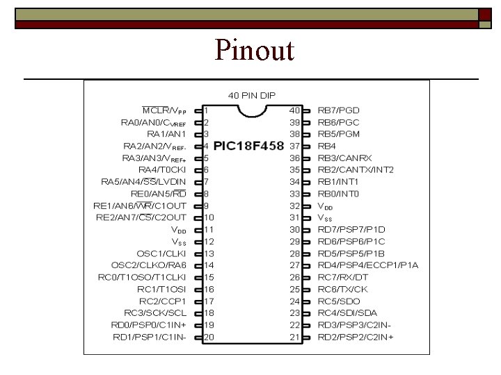
Pinout

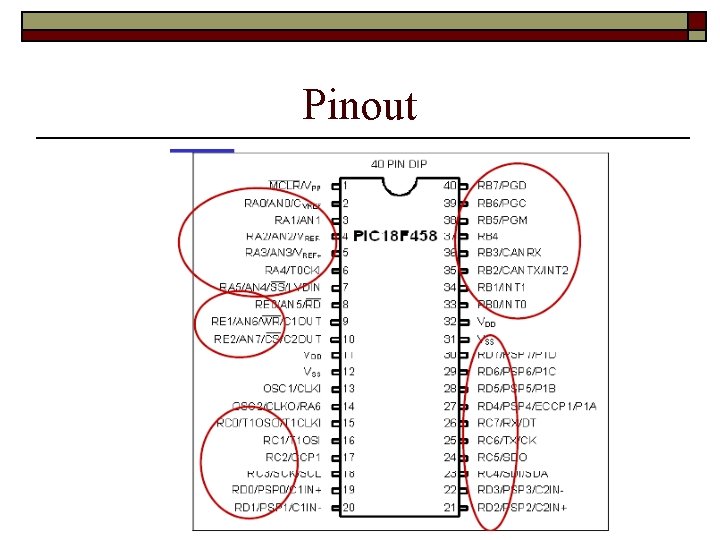
Pinout

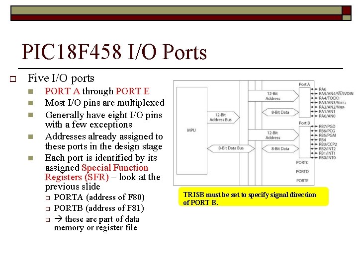
PIC 18 F 458 I/O Ports Five I/O ports PORT A through PORT E Most I/O pins are multiplexed Generally have eight I/O pins with a few exceptions Addresses already assigned to these ports in the design stage Each port is identified by its assigned Special Function Registers (SFR) – look at the previous slide PORTA (address of F 80) PORTB (address of F 81) these are part of data memory or register file TRISB must be set to specify signal direction of PORT B.

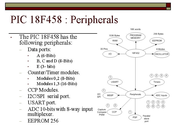
PIC 18 F 458 : Peripherals • The PIC 18 F 458 has the following peripherals: – Data ports: • • • – Counter/Timer modules. • • – – – A (6 -Bits) B, C and D (8 -Bits) E (3 - bits) Modules 0, 2 (8 -Bits) Modules 1, 3 (16 -Bits) CCP Modules. I 2 C/SPI serial port. USART port. ADC 10 -bits with 8 -way input multiplexer. EEPROM 256

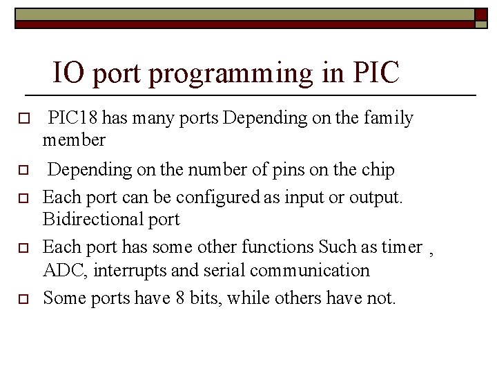
IO port programming in PIC 18 has many ports Depending on the family member Depending on the number of pins on the chip Each port can be configured as input or output. Bidirectional port Each port has some other functions Such as timer , ADC, interrupts and serial communication Some ports have 8 bits, while others have not.

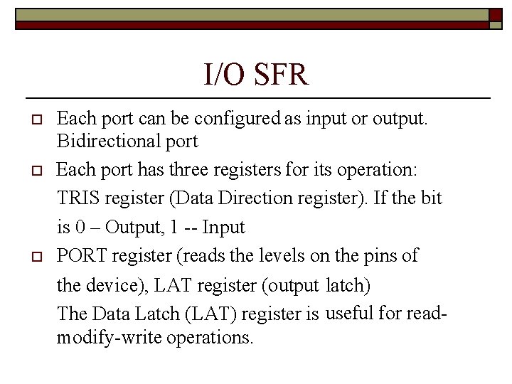
I/O SFR Each port can be configured as input or output. Bidirectional port Each port has three registers for its operation: TRIS register (Data Direction register). If the bit is 0 – Output, 1 -- Input PORT register (reads the levels on the pins of the device), LAT register (output latch) The Data Latch (LAT) register is useful for readmodify-write operations.

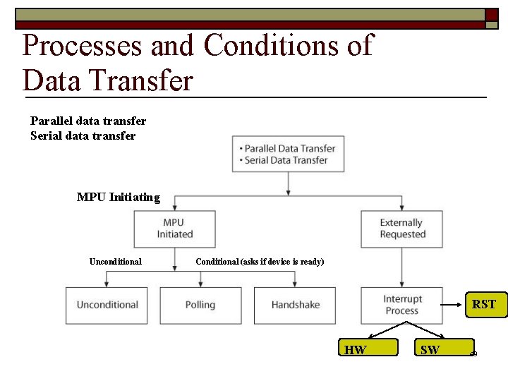
Processes and Conditions of Data Transfer Parallel data transfer Serial data transfer MPU Initiating Unconditional Conditional (asks if device is ready) RST HW SW 49

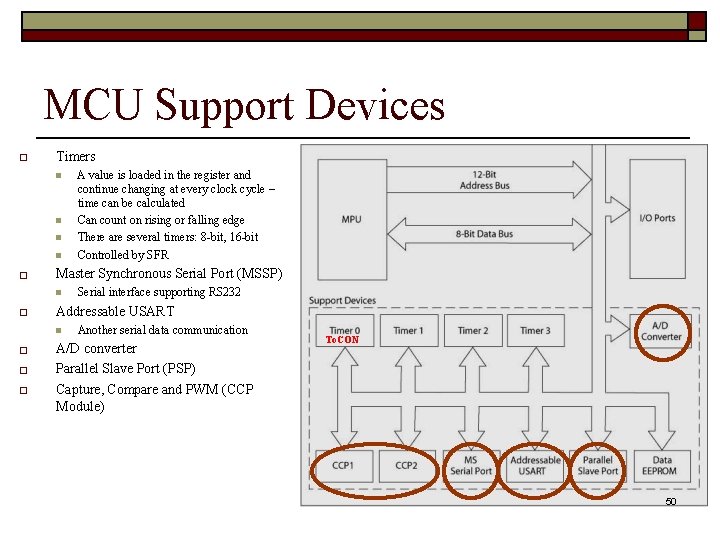
MCU Support Devices Timers Master Synchronous Serial Port (MSSP) Serial interface supporting RS 232 Addressable USART A value is loaded in the register and continue changing at every clock cycle – time can be calculated Can count on rising or falling edge There are several timers: 8 -bit, 16 -bit Controlled by SFR Another serial data communication A/D converter Parallel Slave Port (PSP) Capture, Compare and PWM (CCP Module) To. CON 50

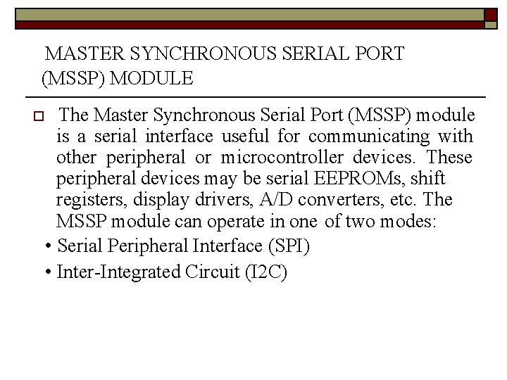
MASTER SYNCHRONOUS SERIAL PORT (MSSP) MODULE The Master Synchronous Serial Port (MSSP) module is a serial interface useful for communicating with other peripheral or microcontroller devices. These peripheral devices may be serial EEPROMs, shift registers, display drivers, A/D converters, etc. The MSSP module can operate in one of two modes: • Serial Peripheral Interface (SPI) • Inter-Integrated Circuit (I 2 C)

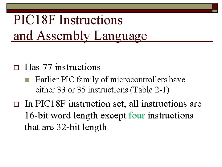
PIC 18 F Instructions and Assembly Language Has 77 instructions Earlier PIC family of microcontrollers have either 33 or 35 instructions (Table 2 -1) In PIC 18 F instruction set, all instructions are 16 -bit word length except four instructions that are 32 -bit length

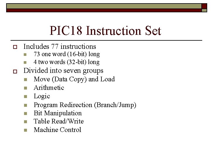
PIC 18 Instruction Set Includes 77 instructions 73 one word (16 -bit) long 4 two words (32 -bit) long Divided into seven groups Move (Data Copy) and Load Arithmetic Logic Program Redirection (Branch/Jump) Bit Manipulation Table Read/Write Machine Control

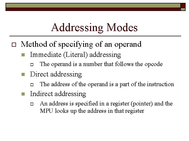
Addressing Modes Method of specifying of an operand Immediate (Literal) addressing Direct addressing The operand is a number that follows the opcode The address of the operand is a part of the instruction Indirect addressing An address is specified in a register (pointer) and the MPU looks up the address in that register

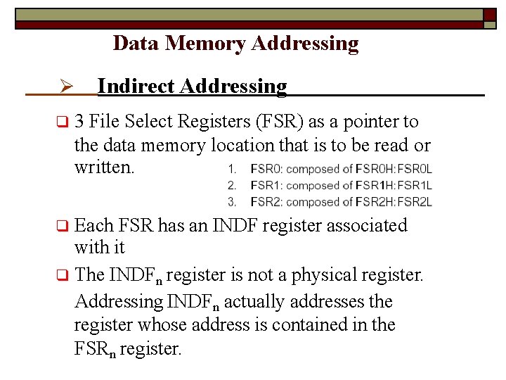
Data Memory Addressing Indirect Addressing 3 File Select Registers (FSR) as a pointer to the data memory location that is to be read or written. Each FSR has an INDF register associated with it The INDFn register is not a physical register. Addressing INDFn actually addresses the register whose address is contained in the FSRn register.

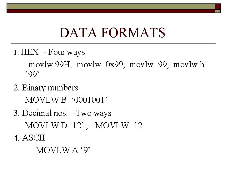
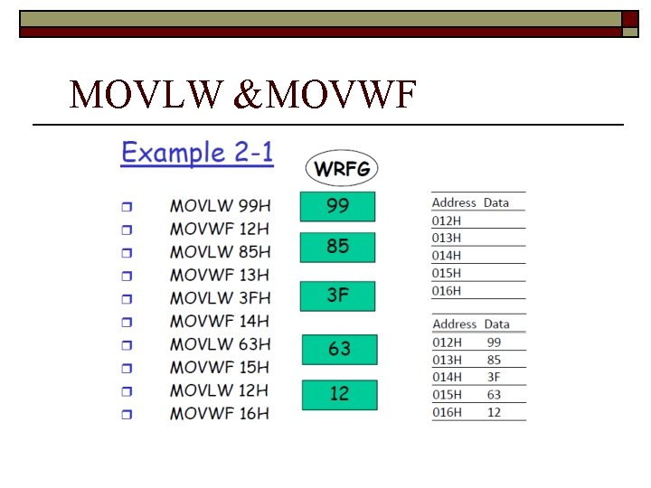
DATA FORMATS 1. HEX - Four ways movlw 99 H, movlw 0 x 99, movlw h ‘ 99’ 2. Binary numbers MOVLW B ‘ 0001001’ 3. Decimal nos. -Two ways MOVLW D ‘ 12’ , MOVLW. 12 4. ASCII MOVLW A ‘ 9’

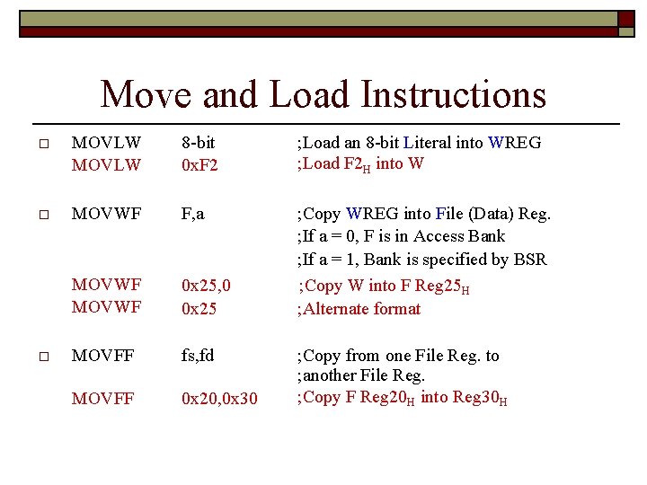
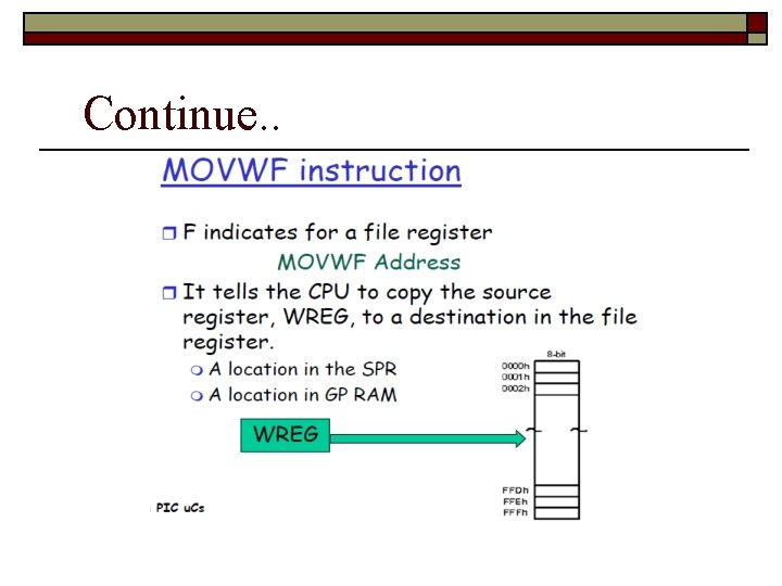
Move and Load Instructions MOVLW 8 -bit 0 x. F 2 ; Load an 8 -bit Literal into WREG ; Load F 2 H into W MOVWF F, a MOVWF 0 x 25, 0 0 x 25 ; Copy WREG into File (Data) Reg. ; If a = 0, F is in Access Bank ; If a = 1, Bank is specified by BSR ; Copy W into F Reg 25 H ; Alternate format MOVFF fs, fd MOVFF 0 x 20, 0 x 30 ; Copy from one File Reg. to ; another File Reg. ; Copy F Reg 20 H into Reg 30 H

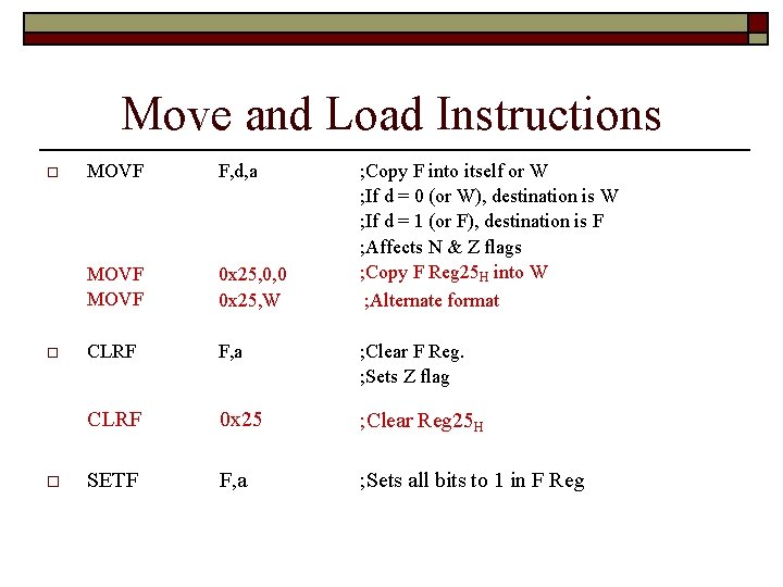
Move and Load Instructions MOVF F, d, a ; Copy F into itself or W ; If d = 0 (or W), destination is W ; If d = 1 (or F), destination is F ; Affects N & Z flags ; Copy F Reg 25 H into W ; Alternate format MOVF 0 x 25, 0, 0 0 x 25, W CLRF F, a ; Clear F Reg. ; Sets Z flag CLRF 0 x 25 ; Clear Reg 25 H SETF F, a ; Sets all bits to 1 in F Reg

Continue. .

MOVLW &MOVWF

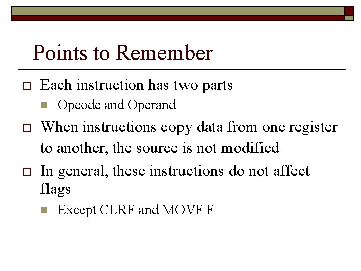
Points to Remember Each instruction has two parts Opcode and Operand When instructions copy data from one register to another, the source is not modified In general, these instructions do not affect flags Except CLRF and MOVF F

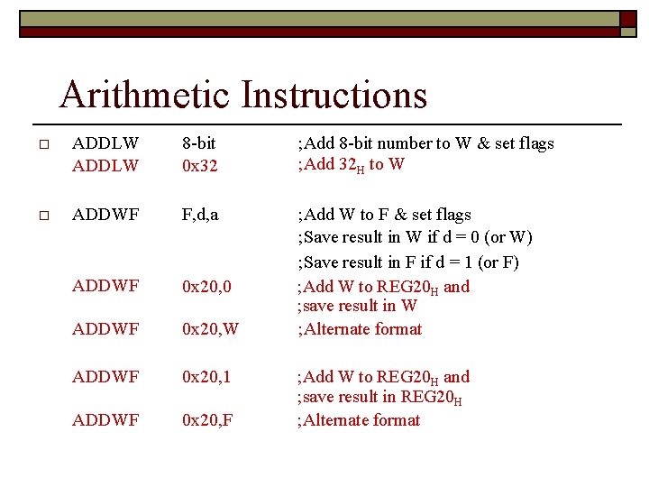
Arithmetic Instructions ADDLW 8 -bit 0 x 32 ; Add 8 -bit number to W & set flags ; Add 32 H to W ADDWF F, d, a ADDWF 0 x 20, 0 ADDWF 0 x 20, W ; Add W to F & set flags ; Save result in W if d = 0 (or W) ; Save result in F if d = 1 (or F) ; Add W to REG 20 H and ; save result in W ; Alternate format ADDWF 0 x 20, 1 ADDWF 0 x 20, F ; Add W to REG 20 H and ; save result in REG 20 H ; Alternate format

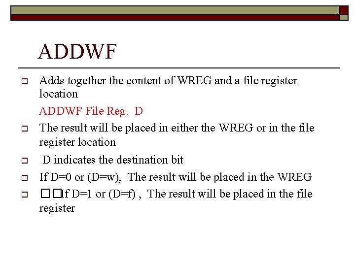
ADDWF Adds together the content of WREG and a file register location ADDWF File Reg. D The result will be placed in either the WREG or in the file register location D indicates the destination bit If D=0 or (D=w), The result will be placed in the WREG ��If D=1 or (D=f) , The result will be placed in the file register

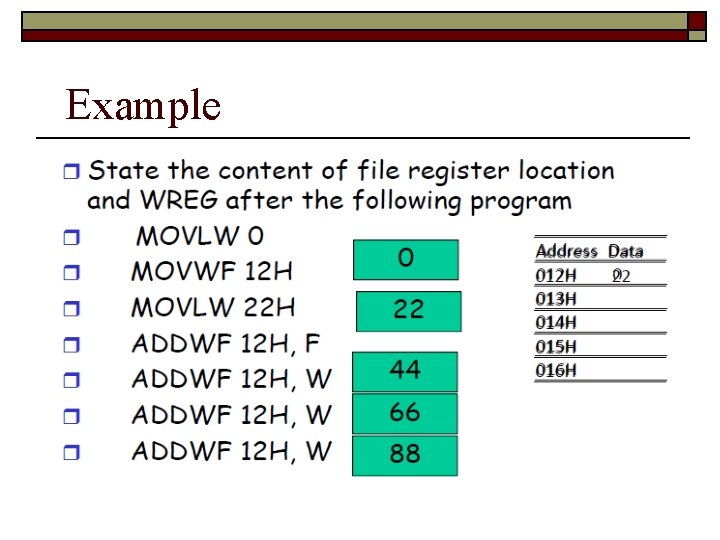
Example

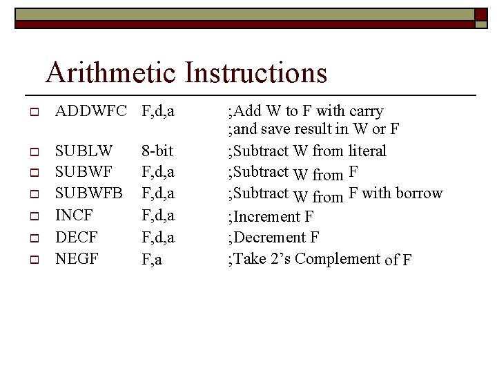
Arithmetic Instructions ADDWFC F, d, a SUBLW SUBWFB INCF DECF NEGF 8 -bit F, d, a F, a ; Add W to F with carry ; and save result in W or F ; Subtract W from literal ; Subtract W from F with borrow ; Increment F ; Decrement F ; Take 2’s Complement of F

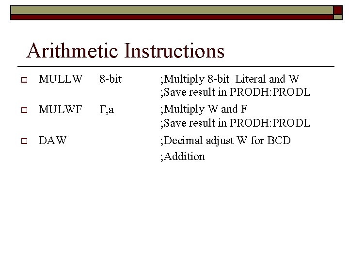
Arithmetic Instructions MULLW 8 -bit MULWF F, a DAW ; Multiply 8 -bit Literal and W ; Save result in PRODH: PRODL ; Multiply W and F ; Save result in PRODH: PRODL ; Decimal adjust W for BCD ; Addition

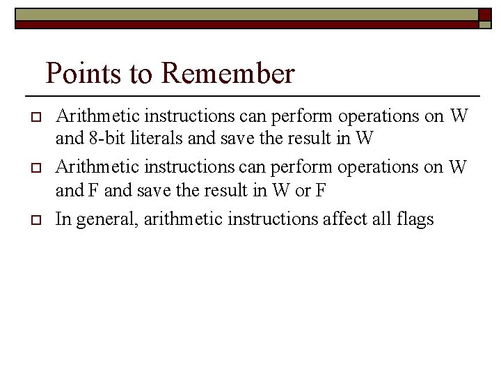
Points to Remember Arithmetic instructions can perform operations on W and 8 -bit literals and save the result in W Arithmetic instructions can perform operations on W and F and save the result in W or F In general, arithmetic instructions affect all flags

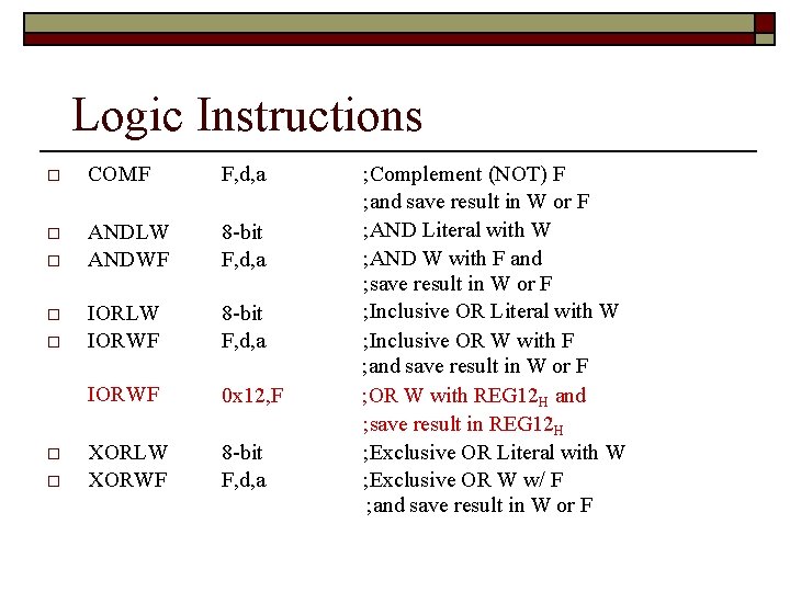
Logic Instructions COMF F, d, a ANDLW ANDWF 8 -bit F, d, a IORLW IORWF 8 -bit F, d, a IORWF 0 x 12, F XORLW XORWF 8 -bit F, d, a ; Complement (NOT) F ; and save result in W or F ; AND Literal with W ; AND W with F and ; save result in W or F ; Inclusive OR Literal with W ; Inclusive OR W with F ; and save result in W or F ; OR W with REG 12 H and ; save result in REG 12 H ; Exclusive OR Literal with W ; Exclusive OR W w/ F ; and save result in W or F

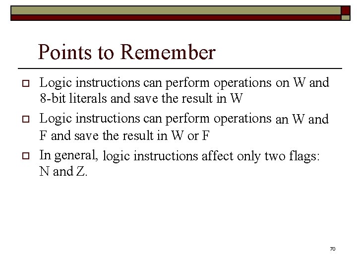
Points to Remember Logic instructions can perform operations on W and 8 -bit literals and save the result in W Logic instructions can perform operations an W and F and save the result in W or F In general, logic instructions affect only two flags: N and Z. 70

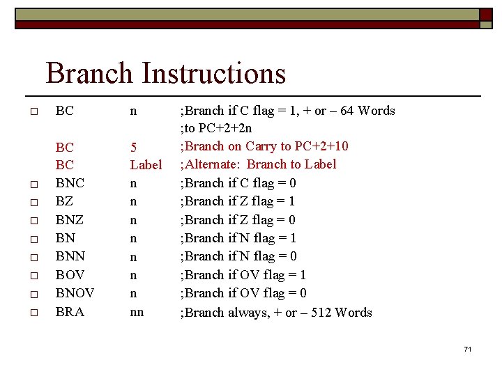
Branch Instructions BC n BC BC BNC BZ BN BNN BOV BNOV BRA 5 Label n n n nn ; Branch if C flag = 1, + or – 64 Words ; to PC+2+2 n ; Branch on Carry to PC+2+10 ; Alternate: Branch to Label ; Branch if C flag = 0 ; Branch if Z flag = 1 ; Branch if Z flag = 0 ; Branch if N flag = 1 ; Branch if N flag = 0 ; Branch if OV flag = 1 ; Branch if OV flag = 0 ; Branch always, + or – 512 Words 71

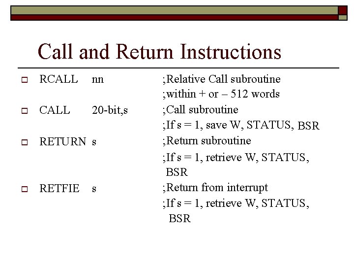
Call and Return Instructions RCALL nn CALL 20 -bit, s RETURN s RETFIE s ; Relative Call subroutine ; within + or – 512 words ; Call subroutine ; If s = 1, save W, STATUS, BSR ; Return subroutine ; If s = 1, retrieve W, STATUS, BSR ; Return from interrupt ; If s = 1, retrieve W, STATUS, BSR

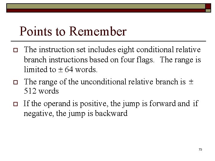
Points to Remember The instruction set includes eight conditional relative branch instructions based on four flags. The range is limited to 64 words. The range of the unconditional relative branch is 512 words If the operand is positive, the jump is forward and if negative, the jump is backward 73

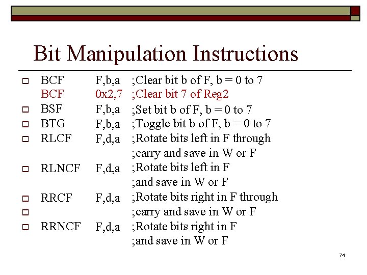
Bit Manipulation Instructions BCF BSF BTG RLCF F, b, a 0 x 2, 7 F, b, a F, d, a RLNCF F, d, a RRNCF F, d, a ; Clear bit b of F, b = 0 to 7 ; Clear bit 7 of Reg 2 ; Set bit b of F, b = 0 to 7 ; Toggle bit b of F, b = 0 to 7 ; Rotate bits left in F through ; carry and save in W or F ; Rotate bits left in F ; and save in W or F ; Rotate bits right in F through ; carry and save in W or F ; Rotate bits right in F ; and save in W or F 74

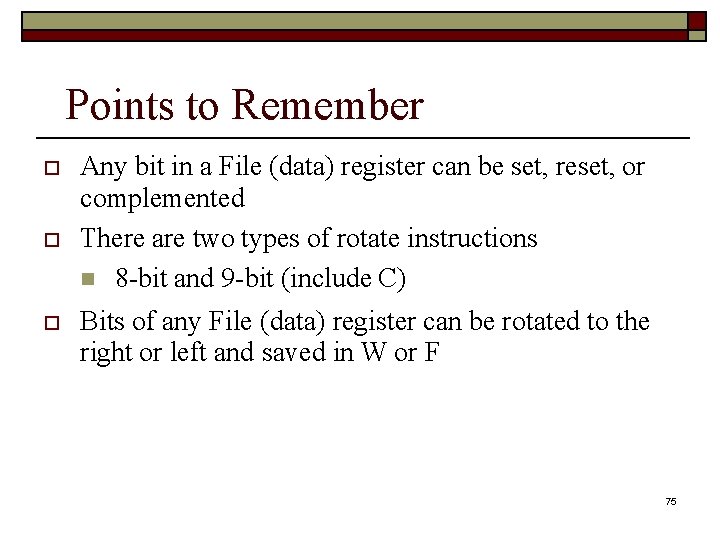
Points to Remember Any bit in a File (data) register can be set, reset, or complemented There are two types of rotate instructions 8 -bit and 9 -bit (include C) Bits of any File (data) register can be rotated to the right or left and saved in W or F 75

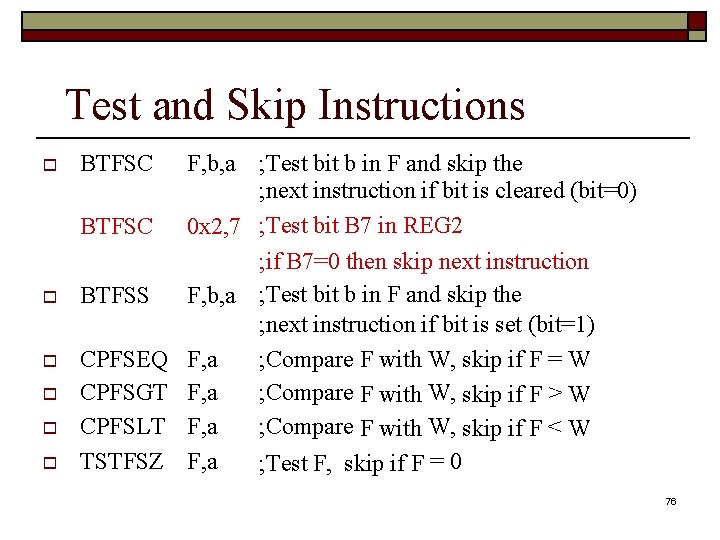
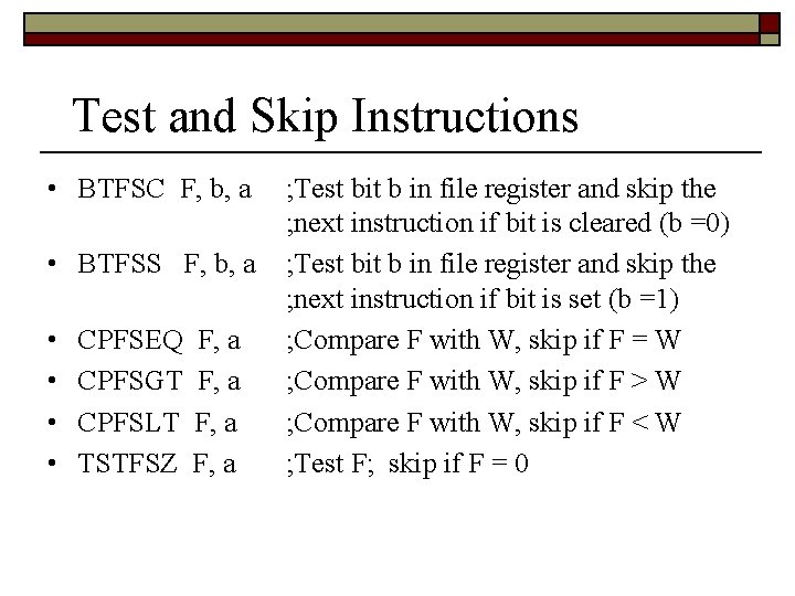
Test and Skip Instructions BTFSC BTFSS CPFSEQ CPFSGT CPFSLT TSTFSZ ; Test bit b in F and skip the ; next instruction if bit is cleared (bit=0) 0 x 2, 7 ; Test bit B 7 in REG 2 ; if B 7=0 then skip next instruction F, b, a ; Test bit b in F and skip the ; next instruction if bit is set (bit=1) F, a ; Compare F with W, skip if F = W F, a ; Compare F with W, skip if F > W F, a ; Compare F with W, skip if F < W F, a ; Test F, skip if F = 0 F, b, a 76

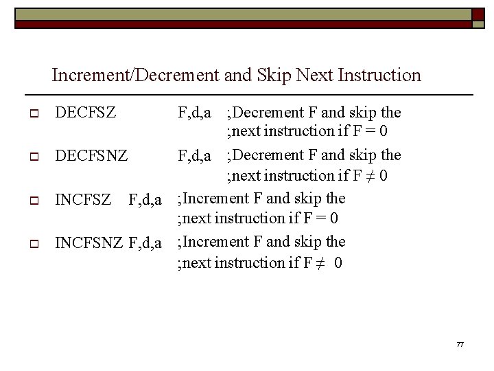
Increment/Decrement and Skip Next Instruction DECFSZ DECFSNZ INCFSNZ F, d, a ; Decrement F and skip the ; next instruction if F = 0 F, d, a ; Decrement F and skip the ; next instruction if F ≠ 0 ; Increment F and skip the ; next instruction if F = 0 ; Increment F and skip the ; next instruction if F ≠ 0 F, d, a 77

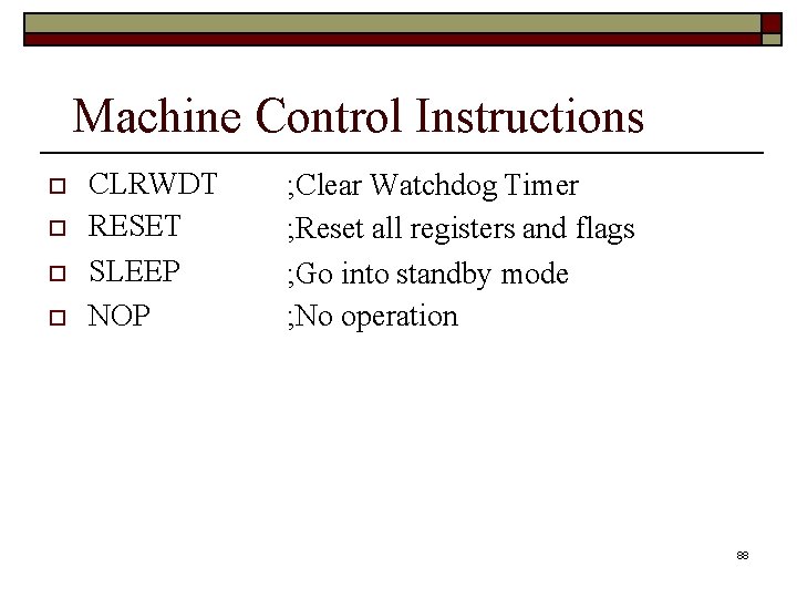
Machine Control Instructions CLRWDT RESET SLEEP NOP ; Clear Watchdog Timer ; Reset all registers and flags ; Go into standby mode ; No operation 88

Test and Skip Instructions • BTFSC F, b, a • BTFSS F, b, a • • CPFSEQ CPFSGT CPFSLT TSTFSZ F, a ; Test bit b in file register and skip the ; next instruction if bit is cleared (b =0) ; Test bit b in file register and skip the ; next instruction if bit is set (b =1) ; Compare F with W, skip if F = W ; Compare F with W, skip if F > W ; Compare F with W, skip if F < W ; Test F; skip if F = 0

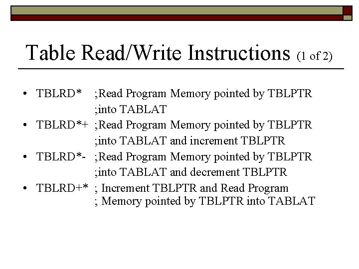
Table Read/Write Instructions (1 of 2) • TBLRD* ; Read Program Memory pointed by TBLPTR ; into TABLAT • TBLRD*+ ; Read Program Memory pointed by TBLPTR ; into TABLAT and increment TBLPTR • TBLRD*- ; Read Program Memory pointed by TBLPTR ; into TABLAT and decrement TBLPTR • TBLRD+* ; Increment TBLPTR and Read Program ; Memory pointed by TBLPTR into TABLAT

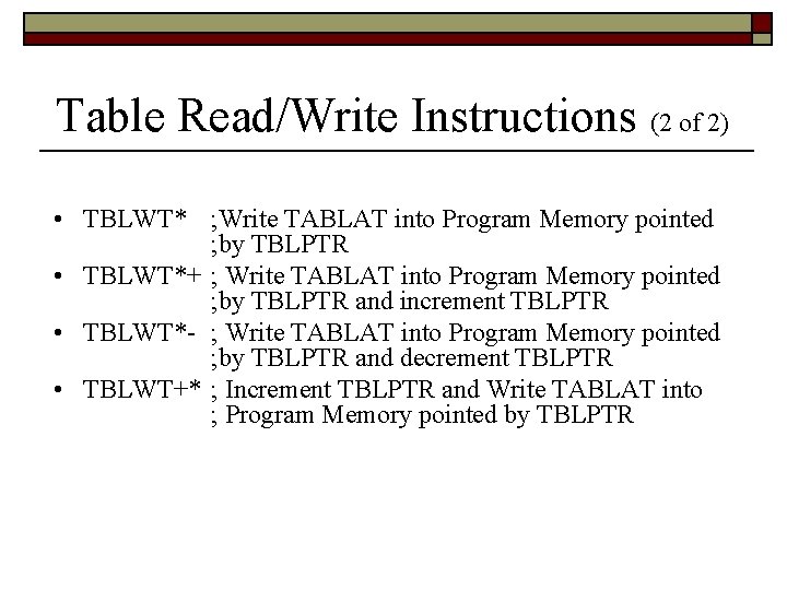
Table Read/Write Instructions (2 of 2) • TBLWT* ; Write TABLAT into Program Memory pointed ; by TBLPTR • TBLWT*+ ; Write TABLAT into Program Memory pointed ; by TBLPTR and increment TBLPTR • TBLWT*- ; Write TABLAT into Program Memory pointed ; by TBLPTR and decrement TBLPTR • TBLWT+* ; Increment TBLPTR and Write TABLAT into ; Program Memory pointed by TBLPTR

Instruction Format (1 of 2) • Byte-oriented instruction – ADDWF F, d, a • Bit-oriented instruction – BCF F, b, a

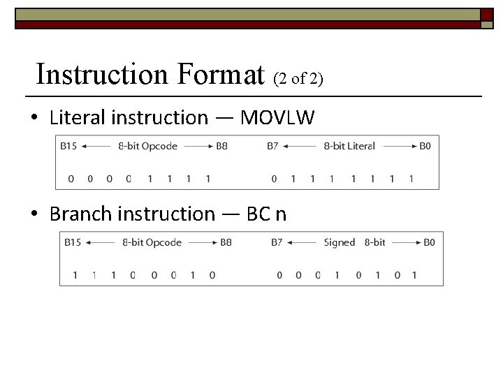
Instruction Format (2 of 2) • Literal instruction — MOVLW • Branch instruction — BC n

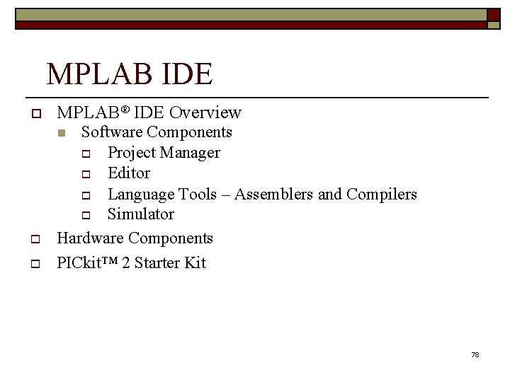
MPLAB IDE MPLAB® IDE Overview Software Components Project Manager Editor Language Tools – Assemblers and Compilers Simulator Hardware Components PICkit™ 2 Starter Kit 78

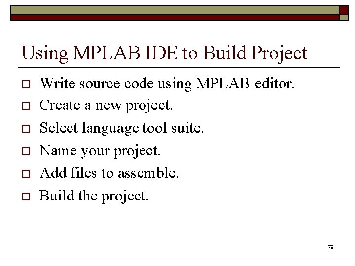
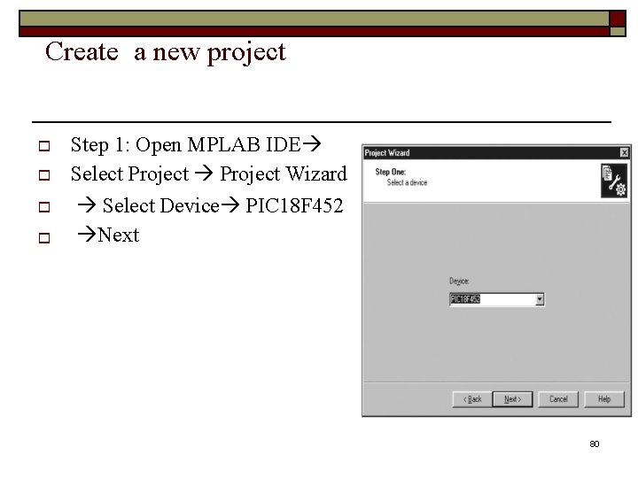
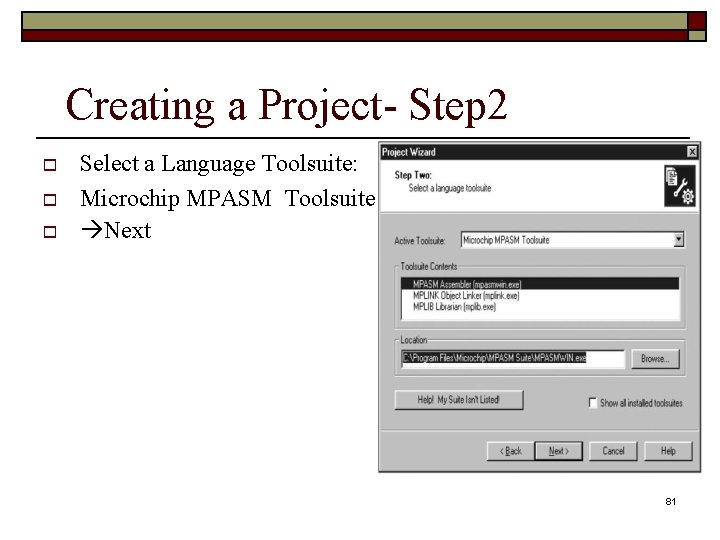
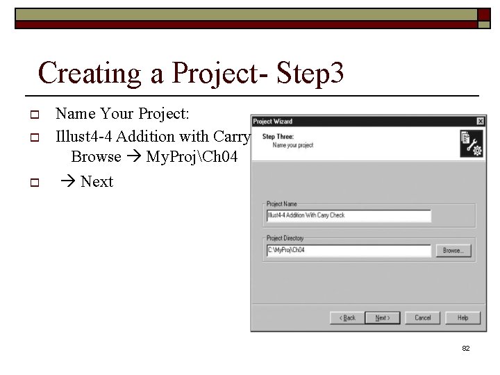
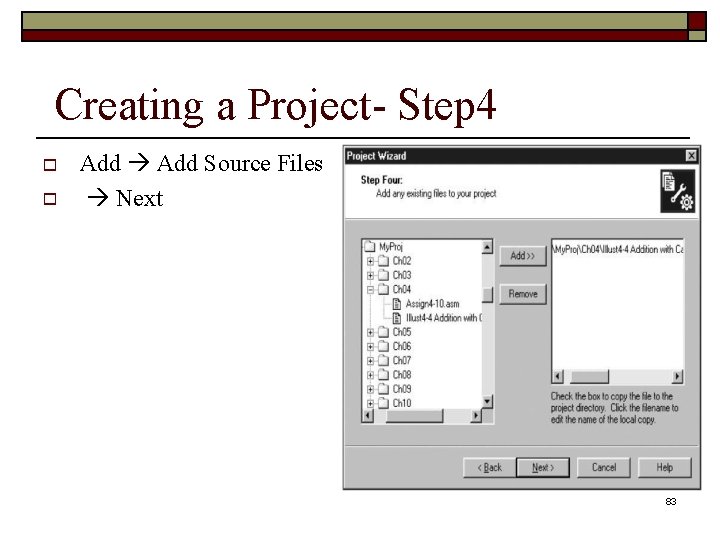
Using MPLAB IDE to Build Project Write source code using MPLAB editor. Create a new project. Select language tool suite. Name your project. Add files to assemble. Build the project. 79

Create a new project Step 1: Open MPLAB IDE Select Project Wizard Select Device PIC 18 F 452 Next 80

Creating a Project- Step 2 Select a Language Toolsuite: Microchip MPASM Toolsuite Next 81

Creating a Project- Step 3 Name Your Project: Illust 4 -4 Addition with Carry Check Browse My. ProjCh 04 Next 82

Creating a Project- Step 4 Add Source Files Next 83

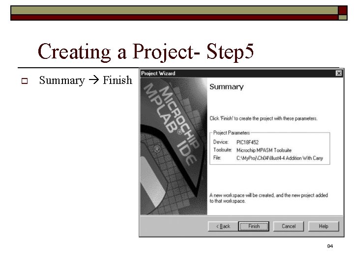
Creating a Project- Step 5 Summary Finish 84

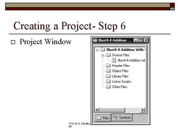
Creating a Project- Step 6 Project Window Prof. M. N. Kakatka r, S. C. O. E. , Pune. 85

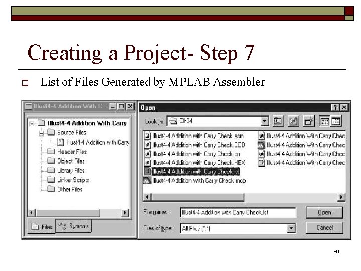
Creating a Project- Step 7 List of Files Generated by MPLAB Assembler 86

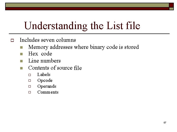
Understanding the List file Includes seven columns Memory addresses where binary code is stored Hex code Line numbers Contents of source file Labels Opcode Operands Comments 87

PIC 18 Simulator Using the Program Memory editor type in the opcode MOVLW 00 and MOWWF TRISC, 0 as described in page 52 of your textbook. Run the program in step-by-step mode and observe the PC. Observe how the NEXT INSTRUCTION changes. What is the value of final clock cycle? How long does it take to complete the program in sec. ? 89