8051 MICROCONTROLLER MODULE IV 992021 1 Content Architecture




- Slides: 64

8051 MICROCONTROLLER MODULE IV 9/9/2021 1

Content • Architecture of 8051 • Special Function Registers(SFRs) • I/O Pins Ports and Circuits • Instruction set • Addressing modes • Assembly language programming. 9/9/2021 2

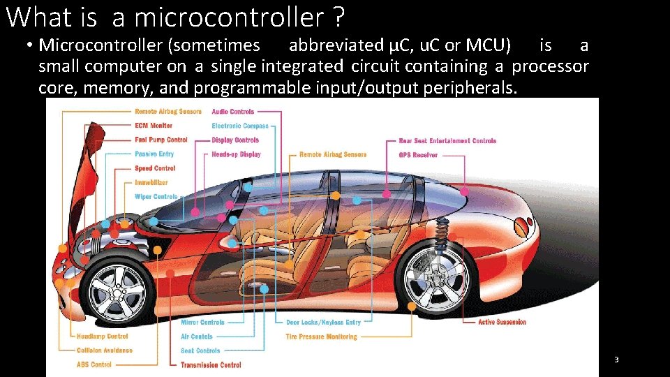
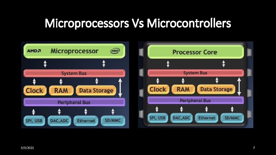
What is a microcontroller ? • Microcontroller (sometimes abbreviated µC, u. C or MCU) is a small computer on a single integrated circuit containing a processor core, memory, and programmable input/output peripherals. 9/9/2021 3

Architecture of 8051 • Features of 8051 • Difference between microprocessor and microcontroller • Pin configuration of 8051 • Architecture of 8051 • Special function registers 9/9/2021 4

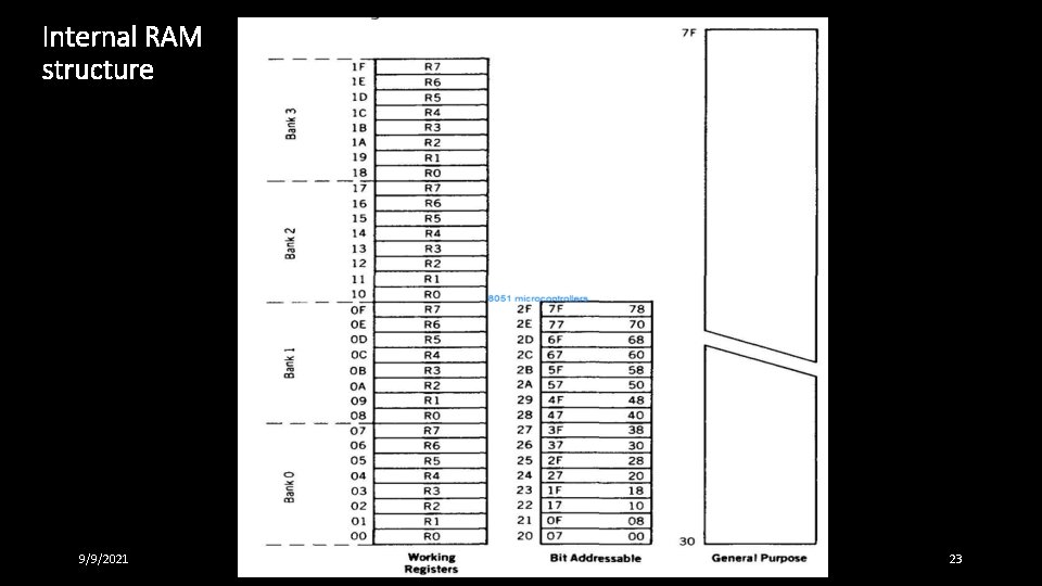
Features of 8051 • 8 bit CPU with registers A and B • 16 bit PC and DPTR(data pointer). • 8 bit program status word(PSW) • 8 bit Stack Pointer • 4 K Internal ROM • 128 bytes Internal RAM 4 register banks each having 8 registers 16 bytes, which may be addressed at the bit level. 80 bytes of general purpose data memory 9/9/2021 5

Features of 8051 • 32 i/o pins arranged as 4 - 8 bit ports: P 0 to P 3 • Two 16 bit timer/counters: T 0 and T 1 • Full duplex serial data receiver/transmitter • Control registers: TCON, TMOD, SCON, PCON, IP and IE • Two external and Three internal interrupt sources. • Oscillator and Clock Circuits. 9/9/2021 6

Microprocessors Vs Microcontrollers 9/9/2021 7

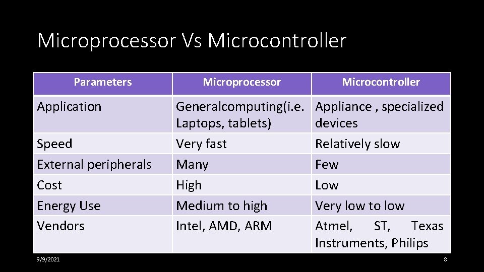
Microprocessor Vs Microcontroller Parameters Application Speed External peripherals Cost Energy Use Vendors 9/9/2021 Microprocessor Microcontroller Generalcomputing(i. e. Laptops, tablets) Very fast Many High Medium to high Intel, AMD, ARM Appliance , specialized devices Relatively slow Few Low Very low to low Atmel, ST, Texas Instruments, Philips 8

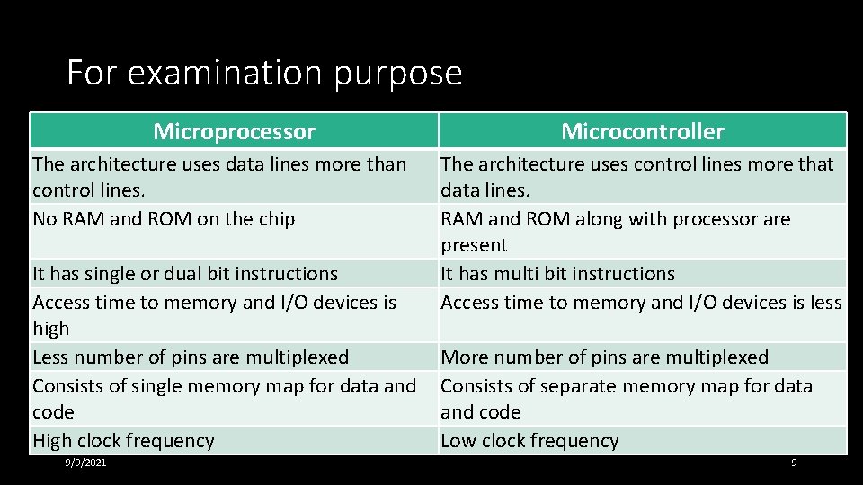
For examination purpose Microprocessor The architecture uses data lines more than control lines. No RAM and ROM on the chip It has single or dual bit instructions Access time to memory and I/O devices is high Less number of pins are multiplexed Consists of single memory map for data and code High clock frequency 9/9/2021 Microcontroller The architecture uses control lines more that data lines. RAM and ROM along with processor are present It has multi bit instructions Access time to memory and I/O devices is less More number of pins are multiplexed Consists of separate memory map for data and code Low clock frequency 9

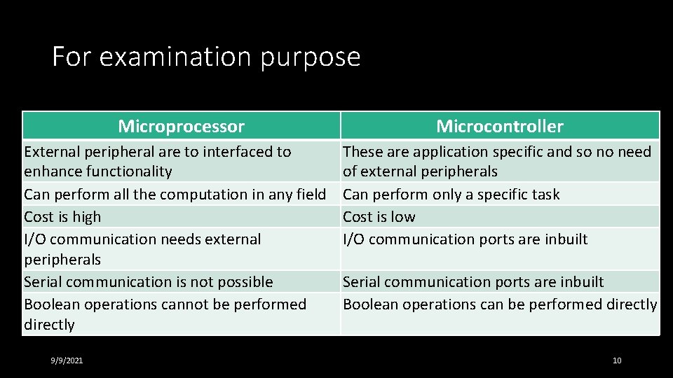
For examination purpose Microprocessor External peripheral are to interfaced to enhance functionality Can perform all the computation in any field Cost is high I/O communication needs external peripherals Serial communication is not possible Boolean operations cannot be performed directly 9/9/2021 Microcontroller These are application specific and so no need of external peripherals Can perform only a specific task Cost is low I/O communication ports are inbuilt Serial communication ports are inbuilt Boolean operations can be performed directly 10

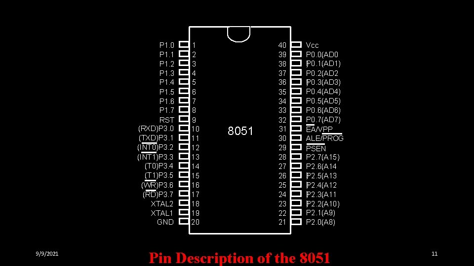
P 1. 0 P 1. 1 P 1. 2 P 1. 3 P 1. 4 P 1. 5 P 1. 6 P 1. 7 RST (RXD)P 3. 0 (TXD)P 3. 1 (INT 0)P 3. 2 (INT 1)P 3. 3 (T 0)P 3. 4 (T 1)P 3. 5 (WR)P 3. 6 (RD)P 3. 7 XTAL 2 XTAL 1 GND 9/9/2021 1 2 3 4 5 6 7 8 9 10 11 12 13 14 15 16 17 18 19 20 8051 40 39 38 37 36 35 34 33 32 31 30 29 28 27 26 25 24 23 22 21 Vcc P 0. 0(AD 0 ) 0. 1(AD 1) P P 0. 2(AD 2 ) 0. 3(AD 3) P P 0. 4(AD 4) P 0. 5(AD 5) P 0. 6(AD 6) P 0. 7(AD 7) EA/VPP ALE/PROG PSEN P 2. 7(A 15) P 2. 6(A 14 )P 2. 5(A 13 )P 2. 4(A 12 )P 2. 3(A 11 ) 2. 2(A 10) P P 2. 1(A 9) P 2. 0(A 8) Pin Description of the 8051 11

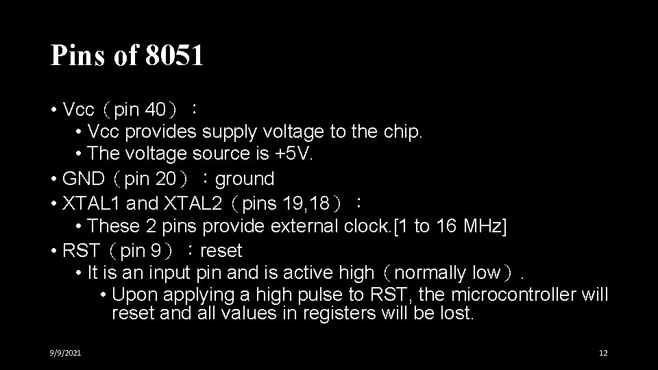
Pins of 8051 • Vcc(pin 40): • Vcc provides supply voltage to the chip. • The voltage source is +5 V. • GND(pin 20):ground • XTAL 1 and XTAL 2(pins 19, 18): • These 2 pins provide external clock. [1 to 16 MHz] • RST(pin 9):reset • It is an input pin and is active high(normally low). • Upon applying a high pulse to RST, the microcontroller will reset and all values in registers will be lost. 9/9/2021 12

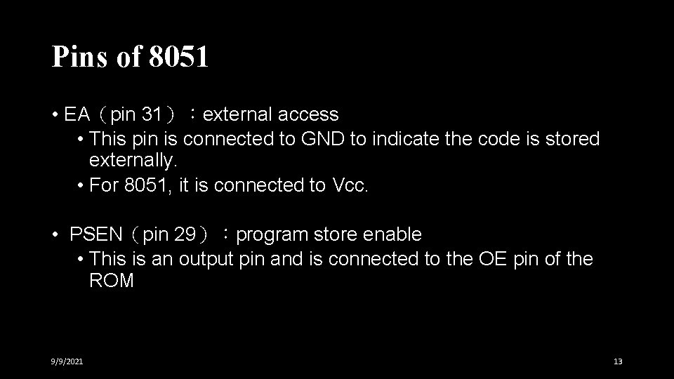
Pins of 8051 • EA(pin 31):external access • This pin is connected to GND to indicate the code is stored externally. • For 8051, it is connected to Vcc. • PSEN(pin 29):program store enable • This is an output pin and is connected to the OE pin of the ROM 9/9/2021 13

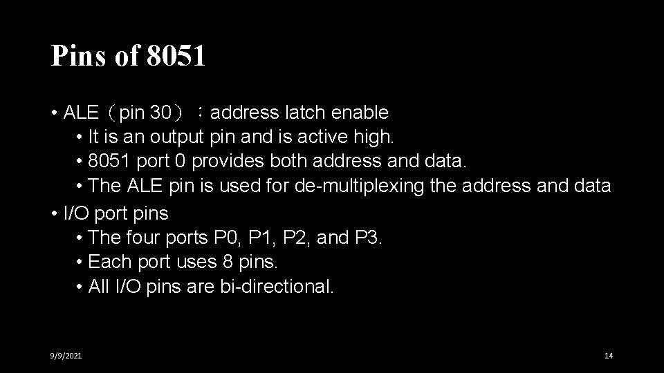
Pins of 8051 • ALE(pin 30):address latch enable • It is an output pin and is active high. • 8051 port 0 provides both address and data. • The ALE pin is used for de-multiplexing the address and data • I/O port pins • The four ports P 0, P 1, P 2, and P 3. • Each port uses 8 pins. • All I/O pins are bi-directional. 9/9/2021 14

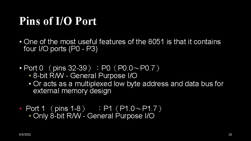
Pins of I/O Port • One of the most useful features of the 8051 is that it contains four I/O ports (P 0 - P 3) • Port 0 (pins 32 -39):P 0(P 0. 0~P 0. 7) • 8 -bit R/W - General Purpose I/O • Or acts as a multiplexed low byte address and data bus for external memory design • Port 1 (pins 1 -8) :P 1(P 1. 0~P 1. 7) • Only 8 -bit R/W - General Purpose I/O 9/9/2021 15

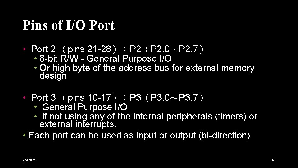
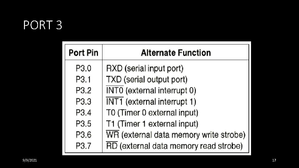
Pins of I/O Port • Port 2 (pins 21 -28):P 2(P 2. 0~P 2. 7) • 8 -bit R/W - General Purpose I/O • Or high byte of the address bus for external memory design • Port 3 (pins 10 -17):P 3(P 3. 0~P 3. 7) • General Purpose I/O • if not using any of the internal peripherals (timers) or external interrupts. • Each port can be used as input or output (bi-direction) 9/9/2021 16

PORT 3 9/9/2021 17

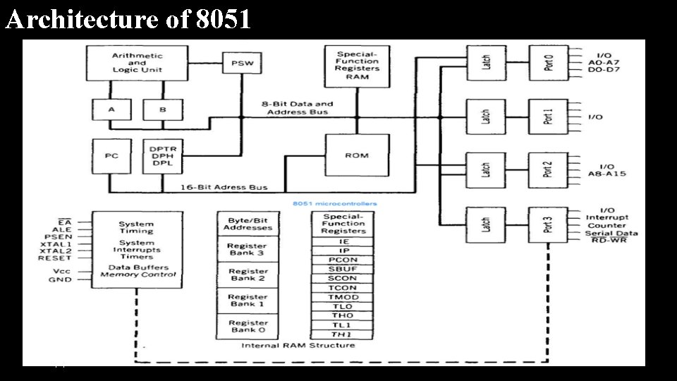
Architecture of 8051 9/9/2021 18

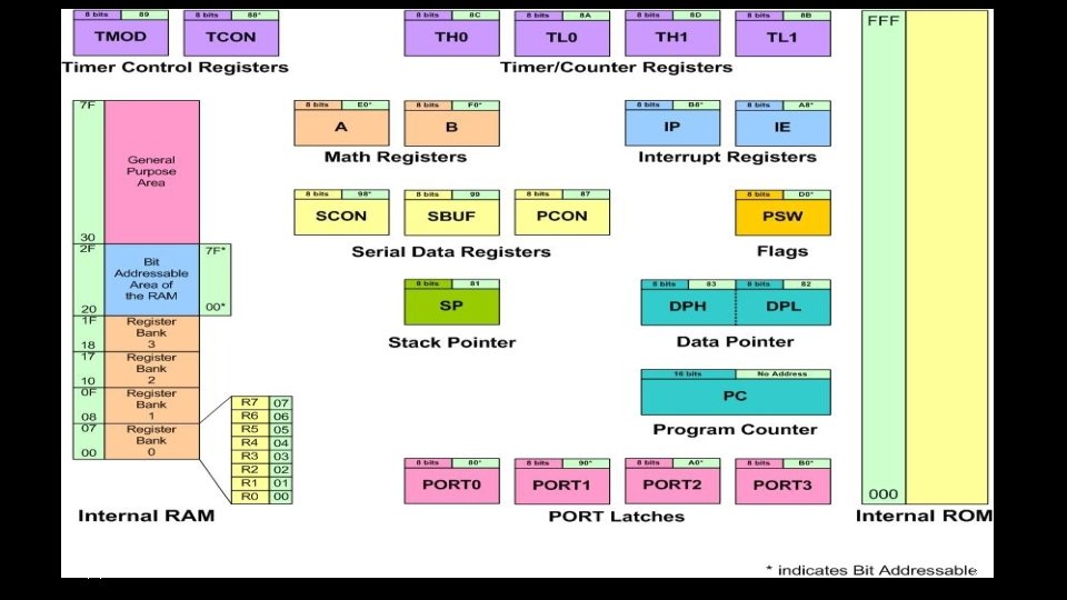
A and B CPU registers • Totally 34 general purpose registers or working registers. • Two of these A and B hold results of many instructions, particularly math and logical operations of 8051 cpu. • The other 32 are in four banks, B 0 – B 3 of eight registers each. • A(accumulator) is used for addition, subtraction, mul, div, boolean bit manipulation and for data transfers. • But B register can only be used for mul and div operations. 9/9/2021 19

Program Counter & Data Pointer • They are both 16 bit registers. • Each is to hold the address of a byte in memory • PC contains the address of the next instruction to be executed. • DPTR is made up of two 8 bit register DPH and DPL; • DPTR contains the address of internal & external code and data that has to be accessed. 9/9/2021 20

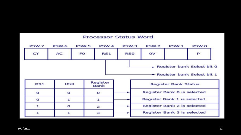
8051 Flag bits and the PSW register 9/9/2021 21

9/9/2021 Programming model 22

Internal RAM structure 9/9/2021 23

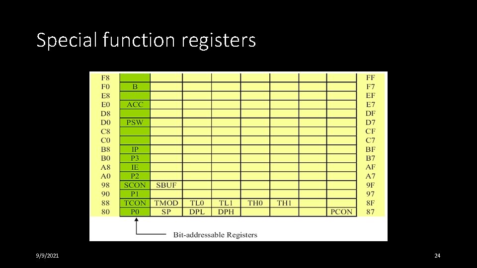
Special function registers 9/9/2021 24

P 0 (Port 0, Address 80 h, Bit-Addressable): • This is input/output port 0. • Each bit of this SFR corresponds to one of the pins on the microcontroller. • For example, bit 0 of port 0 is pin P 0. 0, bit 7 is pin P 0. 7. • Writing a value of 1 to a bit of this SFR will send a high level on the corresponding I/O pin whereas a value of 0 will bring it to a low level. 9/9/2021 25

SP (Stack Pointer, Address 81 h) • This is the stack pointer of the microcontroller. • This indicates where the next value to be taken from the stack will be read from in Internal RAM. • If you push a value onto the stack, the value will be written to the address of SP + 1. • That is to say, if SP holds the value 07 h, a PUSH instruction will push the value onto the stack at address 08 h. • This SFR is modified by all instructions which modify the stack, such as PUSH, POP, LCALL, RETI, and whenever interrupts are provoked by the microcontroller. 9/9/2021 26

DPL/DPH (Data Pointer Low/High, Addresses 82 h/83 h): • The DPL and DPH work together to represent a 16 -bit value called the Data Pointer. • The data pointer is used in operations regarding external RAM and some instructions involving code memory. • Since it is an unsigned two-byte integer value, it can represent values from 0000 to FFFF 9/9/2021 27

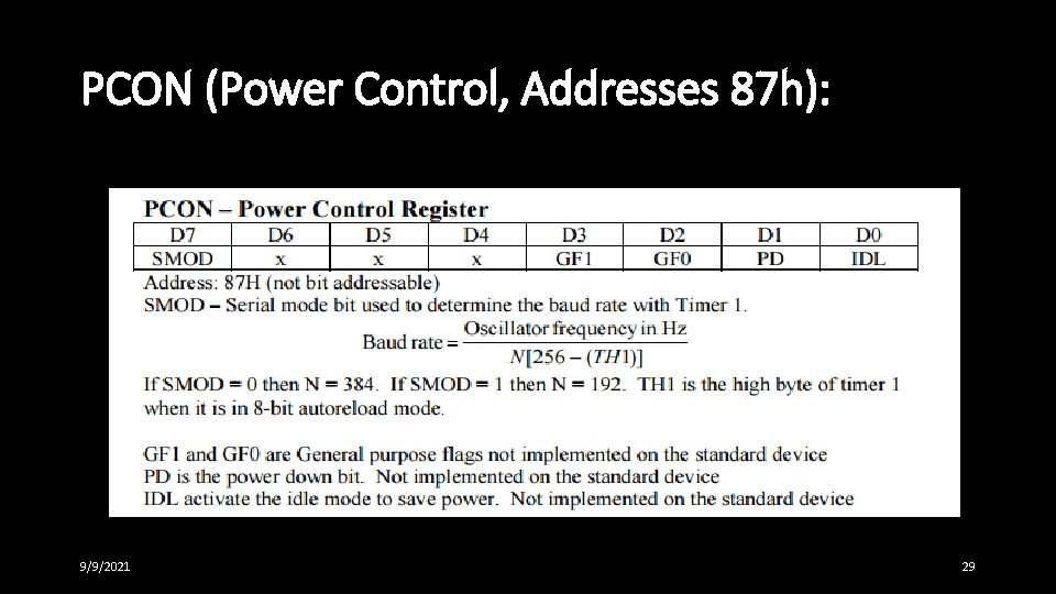
PCON (Power Control, Addresses 87 h): • It is used to control the 8051's power control modes. • Certain operation modes of the 8051 allow the 8051 to go into a type of "sleep" mode which requires much less power. • These modes of operation are controlled through PCON. • Additionally, one of the bits in PCON is used to double the effective baud rate of the 8051's serial port. 9/9/2021 28

PCON (Power Control, Addresses 87 h): 9/9/2021 29

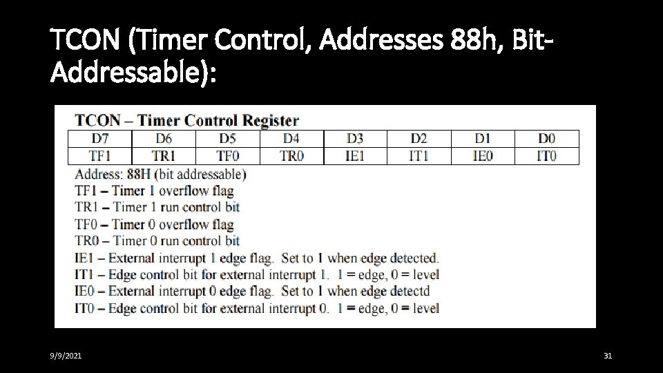
TCON (Timer Control, Addresses 88 h, Bit. Addressable): • It is used to configure and modify the way in which the 8051's two timers operate. • This SFR controls whether each of the two timers is running or stopped • It contains a flag to indicate that each timer has overflowed. • Additionally, some non-timer related bits are located in the TCON SFR. • These bits are used to configure the way in which the external interrupts are activated • It contains the external interrupt flags which are set when an external interrupt has occurred. 9/9/2021 30

TCON (Timer Control, Addresses 88 h, Bit. Addressable): 9/9/2021 31

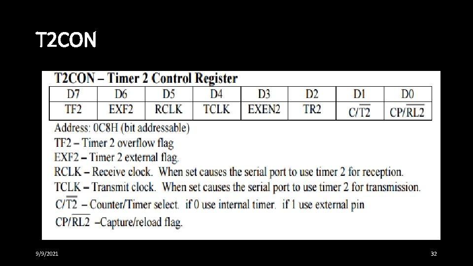
T 2 CON 9/9/2021 32

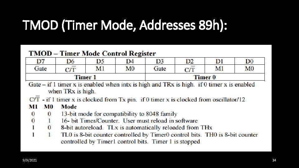
TMOD (Timer Mode, Addresses 89 h): • It is used to configure the mode of operation of each of the two timers. • Using this the program may configure each timer to be a • • 16 -bit timer, an 8 -bit auto reload timer, a 13 -bit timer, or two separate timers. • We may configure the timers to only count when an external pin is activated or • To count "events" that are indicated on an external pin. 9/9/2021 33

TMOD (Timer Mode, Addresses 89 h): 9/9/2021 34

TL 0/TH 0 (Timer 0 Low/High, Addresses 8 Ah/8 Ch): • These two represent timer 0. • Their exact behavior depends on how the timer is configured in the TMOD SFR; • However, these timers always count up. • What is configurable is how and when they increment in value. 9/9/2021 35

TL 1/TH 1 (Timer 1 Low/High, Addresses 8 Bh/8 Dh): • These two together represent timer 1. • Their exact behavior depends on how the timer is configured in the TMOD SFR; • However, these timers always count up. • What is configurable is how and when they increment in value. 9/9/2021 36

P 1 (Port 1, Address 90 h, Bit-Addressable): • This is input/output port 1. • Each bit of this SFR corresponds to one of the pins on the microcontroller. • For example, bit 0 of port 1 is pin P 1. 0, bit 7 is pin P 1. 7. • Writing a value of 1 to a bit of this SFR will send a high level on the corresponding I/O pin whereas a value of 0 will bring it to a low level. 9/9/2021 37

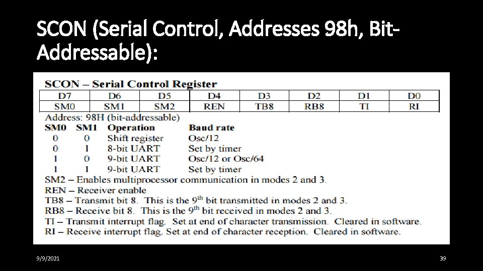
SCON (Serial Control, Addresses 98 h, Bit. Addressable): • It is used to configure the behavior of the 8051's on-board serial port. • This SFR controls the baud rate of the serial port, whether the serial port is activated to receive data, • It contains flags that are set when a byte is successfully sent or received. 9/9/2021 38

SCON (Serial Control, Addresses 98 h, Bit. Addressable): 9/9/2021 39

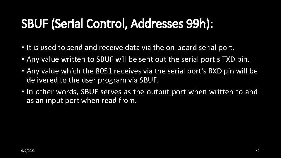
SBUF (Serial Control, Addresses 99 h): • It is used to send and receive data via the on-board serial port. • Any value written to SBUF will be sent out the serial port's TXD pin. • Any value which the 8051 receives via the serial port's RXD pin will be delivered to the user program via SBUF. • In other words, SBUF serves as the output port when written to and as an input port when read from. 9/9/2021 40

P 2 (Port 2, Address A 0 h, Bit-Addressable): • This is input/output port 2. • Each bit of this SFR corresponds to one of the pins on the microcontroller. • For example, bit 0 of port 2 is pin P 2. 0, bit 7 is pin P 2. 7. • Writing a value of 1 to a bit of this SFR will send a high level on the corresponding I/O pin whereas a value of 0 will bring it to a low level. 9/9/2021 41

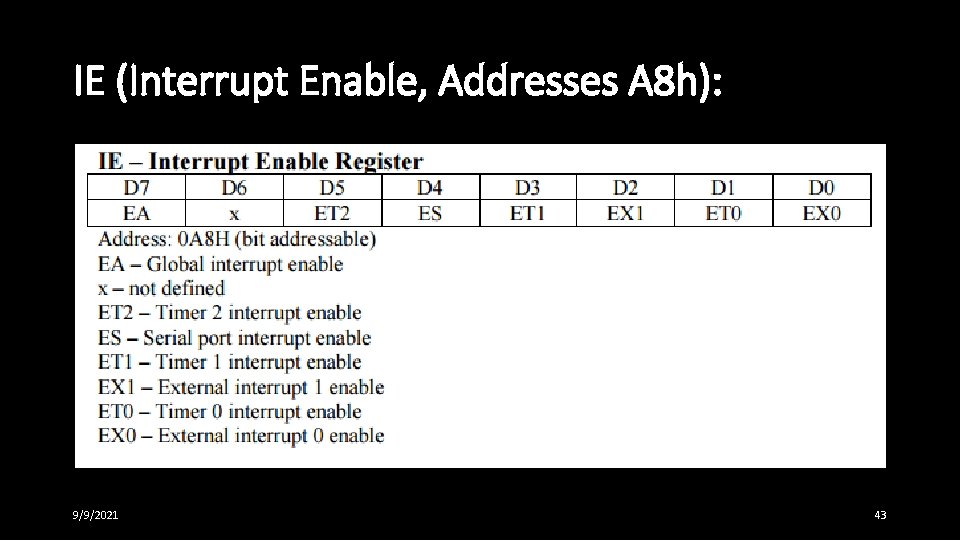
IE (Interrupt Enable, Addresses A 8 h): • It is used to enable and disable specific interrupts. • The low 7 bits of the SFR are used to enable/disable the specific interrupts, • where as the highest bit is used to enable or disable ALL interrupts. • Thus, if the high bit of IE is 0 all interrupts are disabled regardless of whether an individual interrupt is enabled by setting a lower bit. 9/9/2021 42

IE (Interrupt Enable, Addresses A 8 h): 9/9/2021 43

P 3 (Port 3, Address B 0 h, Bit-Addressable): • This is input/output port 3. • Each bit of this SFR corresponds to one of the pins on the microcontroller. • For example, bit 0 of port 3 is pin P 3. 0, bit 7 is pin P 3. 7. • Writing a value of 1 to a bit of this SFR will send a high level on the corresponding I/O pin whereas a value of 0 will bring it to a low level. 9/9/2021 44

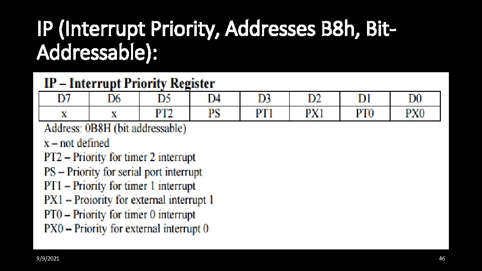
IP (Interrupt Priority, Addresses B 8 h, Bit. Addressable): • It is used to specify the relative priority of each interrupt. • On the 8051, an interrupt may either be of low (0) priority or high (1) priority. • An interrupt may only interrupts of lower priority. • For example, if we configure the 8051 so that all interrupts are of low priority except the serial interrupt, the serial interrupt will always be able to interrupt the system, even if another interrupt is currently executing. • However, if a serial interrupt is executing no other interrupt will be able to interrupt the serial interrupt routine since the serial interrupt routine has the highest priority. 9/9/2021 45

IP (Interrupt Priority, Addresses B 8 h, Bit. Addressable): 9/9/2021 46

PSW (Program Status Word, Addresses D 0 h, Bit-Addressable): • The Program Status Word is used to store a number of important bits that are set and cleared by 8051 instructions. • The PSW SFR contains the carry flag, the auxiliary carry flag, the overflow flag, and the parity flag. • Additionally, the PSW register contains the register bank select flags which are used to select which of the "R" register banks are currently selected. 9/9/2021 47

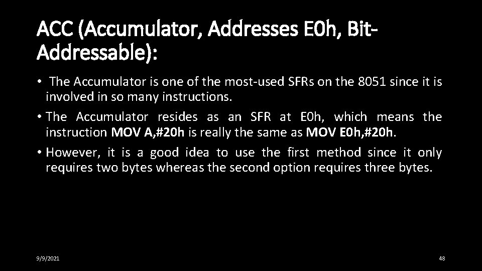
ACC (Accumulator, Addresses E 0 h, Bit. Addressable): • The Accumulator is one of the most-used SFRs on the 8051 since it is involved in so many instructions. • The Accumulator resides as an SFR at E 0 h, which means the instruction MOV A, #20 h is really the same as MOV E 0 h, #20 h. • However, it is a good idea to use the first method since it only requires two bytes whereas the second option requires three bytes. 9/9/2021 48

B (B Register, Addresses F 0 h, Bit. Addressable): • The "B" register is used in two instructions: the multiply and divide operations. • The B register is also commonly used by programmers as an auxiliary register to temporarily store values. 9/9/2021 49

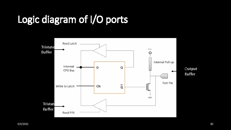
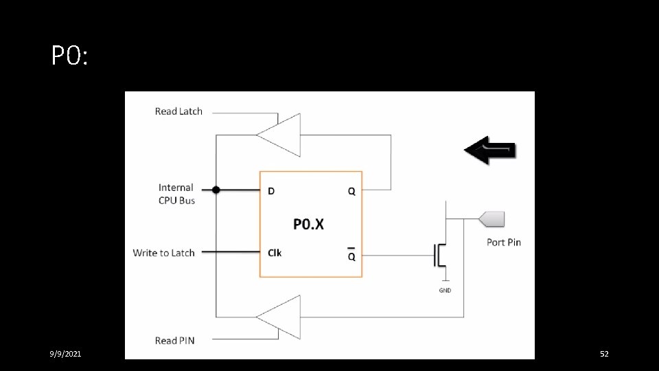
Logic diagram of I/O ports Tristate Buffer Output Buffer Tristate Buffer 9/9/2021 50

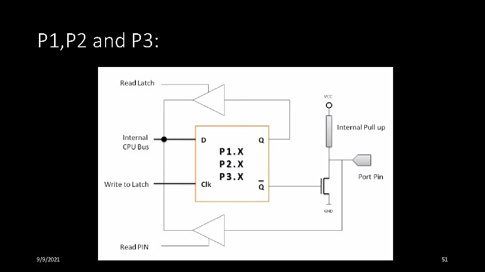
P 1, P 2 and P 3: 9/9/2021 51

P 0: 9/9/2021 52

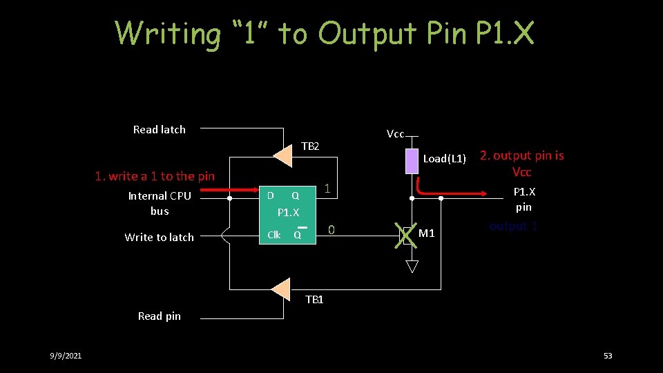
Writing “ 1” to Output Pin P 1. X Read latch Vcc TB 2 1. write a 1 to the pin Internal CPU bus D Write to latch Clk Q Load(L 1) 1 P 1. X pin P 1. X 0 Q 2. output pin is Vcc M 1 output 1 TB 1 Read pin 9/9/2021 53

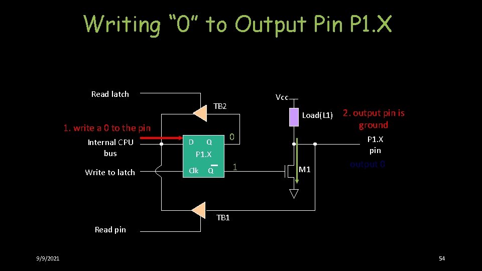
Writing “ 0” to Output Pin P 1. X Read latch Vcc TB 2 1. write a 0 to the pin Internal CPU bus D Write to latch Clk Q Load(L 1) 0 P 1. X pin P 1. X 1 Q 2. output pin is ground M 1 output 0 TB 1 Read pin 9/9/2021 54

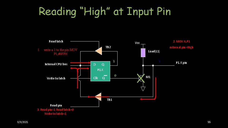
Reading “High” at Input Pin Read latch 1. TB 2 write a 1 to the pin MOV P 1, #0 FFH Internal CPU bus 2. MOV A, P 1 Vcc Load(L 1) D 1 Q 1 external pin=High P 1. X pin P 1. X Write to latch Clk 0 Q M 1 TB 1 Read pin 3. Read pin=1 Read latch=0 Write to latch=1 9/9/2021 55

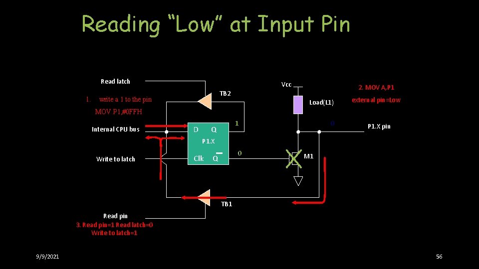
Reading “Low” at Input Pin Read latch 1. Vcc 2. MOV A, P 1 TB 2 write a 1 to the pin Load(L 1) external pin=Low MOV P 1, #0 FFH Internal CPU bus D 1 Q 0 P 1. X pin P 1. X Write to latch Clk 0 Q M 1 TB 1 Read pin 3. Read pin=1 Read latch=0 Write to latch=1 9/9/2021 56

To be continued… 9/9/2021 57

Instruction Set • An instruction is an order or command given to a processor by a computer program. All commands are known as instruction set and set of instructions is known as program. • 8051 have in total 111 instructions, i. e. 111 different words available for program writing. 9/9/2021 58

Instruction Format • Where first part describes WHAT should be done, while other explains HOW to do it. • The latter part can be a data (binary number) or the address at which the data is stored. • Depending upon the number of bytes required to represent 1 instruction completely. 9/9/2021 59

Types Of Instructions are divided into 3 types; 1. One/single byte instruction. 2. Two/double byte instruction. 3. Three/triple byte instruction. 9/9/2021 60

One/single byte instructions • • If operand is not given in the instruction or there is no digits present with instruction, the instructions can be completely represented in one byte opcode. • 9/9/2021 OPCODE 8 bit 61

Two/double byte instruction • If 8 bit number is given as operand in the instruction, the such instructions can be completed represented in two bytes. • First byte OPCODE • Second byte 8 bit data or I/O port 9/9/2021 62

Three/triple byte instruction • If 16 bit number is given as operand in the instructions than such instructions can be completely represented in three bytes 16 bit number specified may be data or address. 9/9/2021 63

Types Of Instructions 1. 2. 3. 4. 5. Data transfer instructions. Arithmetic instructions. Logical instructions with bits. Branch instructions. 9/9/2021 64